

Features
■ Up to 3.5 A step down converter
■ Operating input voltage from 8 V to 55 V
■ 3.3 V and 5.1 V (±1%) fixed output, and
adjustable outputs from:
– 0.5 V to 50 V (3.3 type)
– 5.1 V to 50 V (5.1 type)
■ Frequency adjustable up to 300 kHz
■ Voltage feed forward
■ Zero load current operation (min. 1 mA)
■ Internal current limiting (pulse by pulse and
HICCUP mode)
■ Precise 5.1 V (1.5%) reference voltage
externally available
■ Input/output synchronization function
■ Inhibit for zero current consumption (100 mA
typ. at V
■ Protection against feedback disconnection
■ Thermal shutdown
■ Output over voltage protection
■ Soft-start function
Figure 1. Internal schematic diagram
= 24 V)
CC
VCC (8V to 55V)
C
IN
7
R
OSC
C2
1
4,5,6,10
13,14,15
L4973
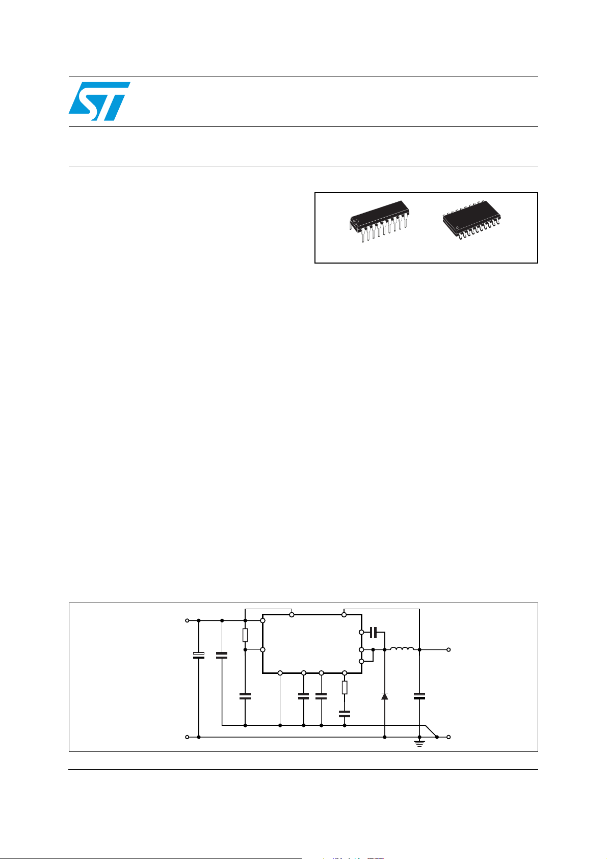
3.5 A step down switching regulator
DIP-18 (12+3+3) SO-20 (12+4+4)
Description
The L4973 is a step down monolithic power
switching regulator delivering 3.5 A at fixed
voltages of 3.3 V or 5.1 V and using a simple
external divider output adjustable voltage up to
50V. Realized in BCD mixed technology, the
device uses an internal power D-MOS transistor
(with a typical R
high efficiency and very fast switching times.
Switching frequency up to 300 kHz are achievable
(the maximum power dissipation of the packages
must be observed).
A wide input voltage range between 8 V to 55 V
and output voltages regulated from 3.3 V to 40 V
cover the majority of the today applications.
Features of this new generation of DC-DC
converter includes pulse by pulse current limit,
hiccup mode for output short circuit protection,
voltage feed forward regulation, soft-start,
input/output synchronization, protection against
feedback loop disconnection, inhibit for zero
current consumption and thermal shutdown.
Packages available are in plastic dual in line, DIP18 (12+3+3) for standard assembly, and SO20
(12+4+4) for SMD assembly.
C
8
L4973
16
12
BOOT
9
3
2
11
17
of 0.15 Ω) to obtain very
DS(on)
VO(3.3V or 5.1V)
L1
R
C
OSC
D97IN554A
COMP
C
SS
C
COMP
D1
C
OUT
February 2009 Rev 18 1/28
www.st.com
28

Contents L4973
Contents
1 Block diagram . . . . . . . . . . . . . . . . . . . . . . . . . . . . . . . . . . . . . . . . . . . . . . 3
2 Pin settings . . . . . . . . . . . . . . . . . . . . . . . . . . . . . . . . . . . . . . . . . . . . . . . . 3
2.1 Pin connection . . . . . . . . . . . . . . . . . . . . . . . . . . . . . . . . . . . . . . . . . . . . . . 3
2.2 Pin description . . . . . . . . . . . . . . . . . . . . . . . . . . . . . . . . . . . . . . . . . . . . . . 4
3 Electrical data . . . . . . . . . . . . . . . . . . . . . . . . . . . . . . . . . . . . . . . . . . . . . . 5
3.1 Maximum ratings . . . . . . . . . . . . . . . . . . . . . . . . . . . . . . . . . . . . . . . . . . . . 5
3.2 Thermal data . . . . . . . . . . . . . . . . . . . . . . . . . . . . . . . . . . . . . . . . . . . . . . . 5
4 Electrical characteristics . . . . . . . . . . . . . . . . . . . . . . . . . . . . . . . . . . . . . 6
5 Evaluation board . . . . . . . . . . . . . . . . . . . . . . . . . . . . . . . . . . . . . . . . . . . . 9
6 Application circuit . . . . . . . . . . . . . . . . . . . . . . . . . . . . . . . . . . . . . . . . . . 12
7 Typical characteristics . . . . . . . . . . . . . . . . . . . . . . . . . . . . . . . . . . . . . . 13
8 Application ideas . . . . . . . . . . . . . . . . . . . . . . . . . . . . . . . . . . . . . . . . . . . 21
9 Package mechanical data . . . . . . . . . . . . . . . . . . . . . . . . . . . . . . . . . . . . 23
10 Order code . . . . . . . . . . . . . . . . . . . . . . . . . . . . . . . . . . . . . . . . . . . . . . . . 26
11 Revision history . . . . . . . . . . . . . . . . . . . . . . . . . . . . . . . . . . . . . . . . . . . 27
2/28

L4973 Block diagram
(x)
1 Block diagram
Figure 2. Block diagram
INH
ZERO CURRENT
INHIBIT
VREF
GOOD
5.1V
3.3V
V5.1
INTERNAL
REFERENCE
INTERNAL
SUPPLY
V
CC
5.1V
V
CC
8(9)7(8)16(18)10(11)
CBOOT
CHARGE
SS
COMP
VFB
SYNC
17(19)
11(12)
5.1V
+
3.3V
E/A
-
12(13)
18(20)
Pin x = Powerdip
= S020
Pin
SOFT
START
THERMAL
SHUTDOWN
-
PWM
+
OSCILLATOR
1(1) 2(2) 3(3)
2 Pin settings
2.1 Pin connection
Figure 3. Pin connection (top view)
HICCUP CURRENT
LIMITING
CURRENT
LIMITING
R
SQQ
4,5,6,13,14,15
(4,5,6,7,14,15,16,17)
DRIVER
BOOT
9(10)
OUTOUTGNDOSC
D94IN161B
OSC
OUT
OUT
GND
GND
GND
V
CC
V
CC
BOOT
1
2
3
4
5
6
7
8
9 INH
D94IN162A
17
16
15
14
13
12
11
10
SYNC18
SS
V5.1
GND
GND
GND
VFB
COMP
OSC
OUT
OUT
GND
GND
GND
GND
V
CC
V
CC
BOOT INH
2
3
4
5
6
7
8
9
10
D94IN163A
DIP -18 (12+3+3) SO20 (12+4+4)
3/28
20
19
18
17
16
15
14
13
12
11
SYNC1
SS
V5.1
GND
GND
GND
GND
VFB
COMP

Pin settings L4973
2.2 Pin description
Table 1. Pin description
N° Pin
Name Description
DIP-18 SO-20
11 12 COMP E/A output to be used for frequency compensation
A logic signal (active high) disables the device (sleep
10 11 INH
mode operation). If not used it must be connected to
GND; if floating the device is disabled.
9 10 BOOT
18 20 SYNC Input/Output synchronization.
7,8 8,9 V
2,3 2,3 OUT Stepdown regulator output.
12 13 VFB
16 18 V5.1 Reference voltage externally available.
4,5,6
13,14,15
1 1 OSC
4,5,6,7
14,15,16,17
CC
GND Signal ground
A capacitor connected between this pin and the output
allows to drive the internal D-MOS.
Unregulated DC input voltage
Stepdown feedback input. Connecting the output
directly to this pin results in an output voltage of 3.3 V
for the L4973V3.3 and 5.1 V for L4973V5.1. An external
resistive divider is required for higher output voltages.
For output voltage resistive divider is required for higher
output voltages. For output voltage less than 3.3 V, see
Note: 1 and Figure 33.
An external resistor connected between the unregulated
input voltage and Pin 1 and a capacitor connected from
Pin 1 to ground fixes the switching frequency. (Line feed
forward is automatically obtained)
Note: 1 The maximum power dissipation of the package must be observed.
4/28

L4973 Electrical data
3 Electrical data
3.1 Maximum ratings
Table 2. Absolute maximum ratings
Symbol
Parameter Value Unit
DIP-18 S0-20
V
V
V
I
V
V
V
V
V
7,V8
2,V3
2,I3
9-V8
V
V
V2,V
I
Input voltage 58 V
9,V8
Output DC voltage
3
Output peak voltage at t = 0.1 μs f = 200 kHz
Maximum output current int. limit.
2,I3
V10-V8 14 V
11
17
12
18
10
V
9
V
V
V
V
V
Bootstrap voltage 70 V
10
Analogs input voltage (V
12
Analogs input voltage (VCC = 24 V) 13 V
19
(VCC = 20 V)
13
(VCC = 20 V)
20
Inhibit
11
= 24 V) 12 V
CC
-0.3
V
-0.3
DIP 12+3+3
Power dissipation a Tpins ≤ 90 °C
= 70 °C no copper area)
(T
P
tot
A
= 70 °C 4 cm copper area on PCB)
(T
A
SO-20
= 90 °C
pins
TJ,T
STG
Power dissipation a T
Junction and storage temperature -40 to 150 °C
-1
- 5
6
V
V
V
V
5.5
0.3
CC
V
V
V
V
5
1.3
2
W
W
W
4W
3.2 Thermal data
Table 3. Thermal data
Symbol Parameter DIP-18 SO-20 Unit
R
thJP
R
thJA
1. Package mounted on board
Maximum thermal resistance junction-pin 12 15 °C/W
Maximum thermal resistance junction-ambient 60
(1)
80
(1)
°C/W
5/28
Electrical characteristics L4973
4 Electrical characteristics
Table 4. Electrical characteristics
(Refer to the test circuit,V
R
= 20 kΩ; unless otherwise specified)
OSC
Symbol Parameter Test condition Min Typ Max Unit
Dynamic characteristics
Input voltage range
Output voltage
L4973V5.1
Output voltage
L4973V3.3
(1)
VO = V
I
I
to 55 V
I
I
to 40 V
= 1 A 5.05 5.1 5.15 V
O
= 0.5 A to 3.5 A VCC = 8 V
O
= 1 A 3.326 3.36 3.393 V
O
= 0.5 A to 3.5 A VCC = 8 V
O
= 24 V; TJ = 25 °C, C
CC
to 40 V; IO = 3.5A
REF
= 2.7 nF;
OSC
(2)
855V
5.00 5.1 5.20 V
(2)
4.95 5.1 5.25 V
3.292 3.36 3.427 V
(2)
3.26 3.36 3.46 V
R
DS(on
)
Maximum limiting
current
η Efficiency
Switching frequency
Supply voltage ripple
rejection
Switching frequency
Δf
stability vs., supply
s
w
voltage
Reference section
Reference voltage
Line regulation
Load regulation
VCC = 10.5 V IO = 3.5 A
= 8 V to 55 V
V
CC
V
= 5.1 V; IO = 3.5 A 90 %
O
= 3.3 V; IO = 3.5 A 85 %
V
O
= VCC+2 V
V
i
= 1 A; f
I
O
V
CC
I
ref
ripple
= 8 V to 55 V 2 5 %
= 0 to 20 mA;
RMS VO
= 100 Hz
= V
VCC = 8 to 55 V
I
= 0 mA;
ref
VCC = 8 to 55 V
V
= 0 to 5 mA;
ref
VCC = 0 to 20 mA
ref
(2)
0.35 Ω
(2)
3.8 4.5 5.5 A
4 4.5 5.5 A
(2)
90 100 110 kHz
;
60 dB
5.025 5.1 5.175 V
(2)
4.950 5.1 5.250 V
5 10 mV
2
1025mV
6
0.15 0.22 Ω
mV
Short circuit current 30 65 100 mA
6/28

L4973 Electrical characteristics
Table 4. Electrical characteristics (continued)
(Refer to the test circuit,V
R
= 20 kΩ; unless otherwise specified)
OSC
Symbol Parameter Test condition Min Typ Max Unit
Soft-start
Soft-start charge current 30 45 60 μA
= 24 V; TJ = 25 °C, C
CC
= 2.7 nF;
OSC
Soft-start discharge
current
Inhibit
High level voltage
Low level voltage
high level V
I
source
I
low level V
source
DC characteristics
Total operating
quiescent current
Quiescent current Duty cycle = 0 2.7 4 mA
Total stand-by quiescent
current
Error amplifier
High level output voltage 11.0 V
Low level output voltage 0.65 V
Source bias current 1 2 3 μA
Source output current 200 300 600 μA
Sink output current 200 300 μA
15 22 30 μA
(2)
3.0 V
= 3 V
INH
= 0.8 V
INH
(2)
(2)
10 16 50 μA
(2)
10 15 50 μA
0.8 V
Duty cycle = 50 % 4 6 mA
V
CC
V
CC
= 24 V; V
= 55 V; V
= 5 V 100 200 μA
INH
= 5 V 150 300 μA
INH
Supply voltage ripple
rejection
DC open loop gain R
Transconductance
Oscillator section
Ramp valley 0.78 0.85 0.92 V
Ramp peak
Maximum duty cycle 95 97 %
= VFB
V
COMP
C
= 4.7 μF 1-5 mA load
REF
60 80 dB
current
= ∞ 50 60 dB
L
I
= -0.1 to 0.1 mA;
comp
= 6 V
V
comp
V
= 8 V
CC
VCC = 55 V
1.992.1
2.5 mS
2.3
9.6
10.2VV
7/28

Electrical characteristics L4973
Table 4. Electrical characteristics (continued)
(Refer to the test circuit,V
R
= 20 kΩ; unless otherwise specified)
OSC
Symbol Parameter Test condition Min Typ Max Unit
= 24 V; TJ = 25 °C, C
CC
= 2.7 nF;
OSC
Maximum frequency
Sync function
High input voltage VCC = 8 V to 55 V 3.5 V
Low input voltage V
Slave sink current 0.15 0.25 0.45 mA
Master output amplitude I
Output pulse width No load, V
1. Pulse testing with a low duty cycle
2. Specifications referred to T
from -40 °C to 125 °C.
J
Duty cycle = 0%;
R
=13 kΩ; C
OSC
= 8 V to 55 V 0.9 V
CC
= 3 mA 4 4.5 V
source
sync
= 820 pF;
OSC
= 4.5 V 0.20 0.35 μs
300 kHz
8/28

L4973 Evaluation board
5 Evaluation board
Figure 4. Evaluation board circuit
SYNCHSYNCH
U1
U1
OSC
SS
V5.1
L4973 DIP 18
L4973 DIP 18
R5NMR5
NM
3
8
VCC7VCC
JP1JP1
2
10
INH
COMP
11
C4
22nC422n
C5
R2
150pC5150p
15kR215k
VinVin
470u 63v
470u 63v
GNDGND
R1
15kR115k
C10
C10
C9
220nC9220n
C2
C1
470nC2470n
2.7nC12.7n
1
17
16
C3A1uC3A
C3NMC3
1u
NM
Table 5. Component list (fsw = 150 kHz, V
18
SYNC
R6 NMR6 NM
1
C8 220nC8 220n
9
2
OUT
3
BOOT
OUT
15
GND
GND
GND
GND
GND
GND
VFB
12
signal GND
GND plane
14
13
6
5
4
OUT
Q2NMQ2
NM
signal GND
= 5 V)
L1 68uHL1 68uH
R7NMR7
NM
D1
STPS5L60D1STPS5L60
1 2
C6NMC6
NM
C11
C11
C7NMC7
NM
150u 50v
150u 50v
C12
C12
150u 50v
150u 50v
VoutVout
R3
2.7kR32.7k
C14NMC14
NM
C13NMC13
NM
R4
4.99kR44.99k
GNDGND
Reference Description Part number Manufacturer
R1 Resistor 15 kΩ 1%
R2 Resistor 15 kΩ 1%
R3 Resistor 2.7 kΩ 1%
R4 Resistor 4.99 kΩ 1%
R5 Not mounted
R6 Not mounted
R7 Not mounted
C1 Capacitor 2.7 nF 5%
C2 Capacitor 470 nF 5%
C3 Capacitor 1 μF 5%
C4 Capacitor 22 nF 5%
C5 Capacitor 150 pF 5%
C6 Not mounted
C7 Not mounted
C8 Capacitor 220 nF 5%
C9 Capacitor 220 nF 5%
C10 Capacitor 470 μF 63V EKY-630ELL471ML20S Nippon Chemi-con
9/28

Evaluation board L4973
Table 5. Component list (fsw = 150 kHz, V
Reference Description Part number Manufacturer
C11 Capacitor 150 μF 35 V EKY-350ELL151MHB5D Nippon Chemi-con
C11 Capacitor 150 μF 35 V EKY-350ELL151MHB5D Nippon Chemi-con
C13 Capacitor 100 nF 5 %
C14 Not mounted
L1 68 μH I
U1 L4973V3.3 STMicroelectronics
RMS
= 3.4 A I
Table 6. Resistor divider for V
Reference Description Part number Manufacturer
R3 Resistor 2.7 kΩ 1%
R4 Resistor 1 kΩ 1%
Table 7. Resistor divider for V
Reference Description Part number Manufacturer
R3 Resistor 2.7 kΩ 1%
R4 Not mounted
= 6.7 A DO5040H-683MLD Coilcraft
SAT
= 12 V
OUT
= 3.3 V
OUT
= 5 V) (continued)
OUT
10/28

L4973 Evaluation board
Figure 5. Evaluation board (components side)
Figure 6. Evaluation board (solder side)
11/28

Application circuit L4973
6 Application circuit
Figure 7. Application circuit (see Figure 4 part list)
V
CC
INH SYNC
9
2,3
12
D1
C1 C2R2C7
7,8 10 18
1
17
L4973V5.1
11
4,5,6
13,14,15
R1
C6
D97IN665A
16
C3
C4 C5
Figure 8. Application circuit (see Figure 4 part list)
V
CC
C1 C2R2C7
C3
C4 C5
INH SYNC
7,8 10 18 9
1
17
L4973V3.3
11
13,14,15
R1
C6
D97IN664A
4,5,6
12
16
2,3
D1
C8
L1
3 x
C0
C8
L1
3 x
C0
Vo
C12
Vo
C12
12/28

L4973 Typical characteristics
)
)
7 Typical characteristics
Figure 9. Quiescent drain current vs.
Ibias
(mA)
5.0
4.5
4.0
3.5
3.0
2.5
input voltage (0% duty cycle)
D97IN633A
200KHz-R2=22K
C7=1.2nF
Tamb=25˚C
0% DC
100KHz-R2=20K
C7=2.7nF
0Hz
Figure 10. Quiescent drain current vs.
junction temperature
Ibias
(mA)
4.0
3.5
3.0
0% DC
V
CC
= 35V
200KHz-R2=22K
C7=1.2nF
100KHz-R2=20K
C7=2.7nF
0Hz
D97IN634
2.0
0 1020304050VCC(V)
Figure 11. Stand by drain current vs.
Ibias
(μA)
150
100
50
input voltage
D97IN635A
V
= 5V
inh
25˚C
125˚C
0 1020304050VCC(V)
2.5
-50 0 50 100 Tj(˚C
Figure 12. Reference voltage vs.
junction temperature (pin 16)
V
REF
(V)
5.15
Vcc=35V
5.1
5.05
5.0
-20 20 60 100
-40 0 40 80 Tj(˚C
D97IN637
Pin 16
13/28

Typical characteristics L4973
)
Figure 13. Reference voltage vs.
V
REF
(V)
5.15
5.1
5.05
5.0
input voltage (pin 16)
D97IN636A
Tj=25˚C
Pin 16
0 1020304050VCC(V)
Figure 15. Inhibit current vs. inhibit
Iinh
(μA)
100
voltage (pin 10)
Vcc=35V
Pin 10
D97IN651
Tj=0˚C
Figure 14. Reference voltage vs.
reference input current
V
REF
(V)
5.2
Vcc=40V
5.1
5.0
4.9
0 1020304050I
Vcc=10V
Tj=25˚C
D97IN638
REF
(mA)
Figure 16. Line regulation (see Figure 7)
V
(V)
5.12
O
Tj=125˚C
D97IN639A
Tj=25˚C
50
Tj=125˚C
0
-50
0 15 Vinh(V
105
5.1
5.08
5.06
0 1020304050VCC(V)
Tj=25˚C
IO = 1A
14/28

L4973 Typical characteristics
Figure 17. Load regulation (see
V
O
(V)
5.15
5.1
5.05
5.0
Figure 7)
D97IN640
VCC = 35V
Tj=125˚C
Tj=25˚C
0123I
(A)
O
Figure 19. Load regulation (see
V
O
(V)
3.35
3.34
3.33
3.32
3.31
Figure 4)
D97IN661
VCC = 35V
Tj=125˚C
Tj=25˚C
Figure 18. Line regulation (see Figure 8)
V
O
(V)
3.35
3.34
3.33
3.32
3.31
3.3
0 1020304050VCC(V)
D97IN660A
Tj=125˚C
Tj=25˚C
IO = 1A
Figure 20. Switching frequency vs.
R2 and C7 (Figure 4)
fsw
(KHz)
500
200
100
50
20
10
0.82nF
1.2nF
2.2nF
3.3nF
5.6nF
D97IN630
Tamb=25˚C
4.7nF
3.3
0123I
5
(A)
O
0 20 40 60 80 R2(KΩ)
15/28

Typical characteristics L4973
)
Figure 21. Switching frequency vs.
input voltage
fsw
D97IN631
(KHz)
Tamb=25˚C
105
100
95
90
0 1020304050VCC(V)
Figure 23. Dropout voltage between pin
ΔV
(V)
0.6
0.4
0.2
0
7,8 and 2,3
D97IN643
Tj=125˚C
Tj=25˚C
Tj=0˚C
0123I
(A)
O
Figure 22. Switching frequency vs.
junction temperature
(see Figure 4)
fsw
(KHz)
105
100
95
90
-50 0 50 100 Tj(˚C
D97IN632
Figure 24. Efficiency vs. output voltage
(see Figure 6)
η
(%)
98
96
100KHz
94
200KHz
92
90
88
86
0102030 VO(V)40
IO = 3A
V
CC
D97IN641
= 50V
16/28

L4973 Typical characteristics
Figure 25. Dropout voltage between pin
ΔV
(V)
0.6
0.4
0.2
0
7,8 and 2,3
D97IN643
Tj=125˚C
Tj=25˚C
Tj=0˚C
0123I
(A)
O
Figure 27. Efficiency vs. output voltage
η
(%)
98
96
94
92
(Diode STPS745D)
D97IN642
100KHz
200KHz
Figure 26. Efficiency vs. output voltage
(see Figure 4)
η
(%)
98
96
100KHz
94
200KHz
92
90
88
86
0102030 VO(V)40
IO = 3A
V
CC
D97IN641
= 50V
Figure 28. Efficiency vs. output current
(see Figure 7)
η
(%)
95
90
Vcc=12V
Vcc=24V
VO = 5.1V
= 100KHz
f
sw
D97IN645
90
88
IO = 3A
V
CC
= 35V
86
0101520 V
O
(V)30525
85
80
0123I
Vcc=48V
(A)
O
17/28

Typical characteristics L4973
)
Figure 29. Efficiency vs. output current
η
(%)
90
85
80
75
(see Figure 7)
D97IN646
Vcc=12V
Vcc=24V
Vcc=48V
VO = 5.1V
= 200KHz
f
sw
0123I
(A)
O
Figure 31. Efficiency vs. output current
(see Figure 8)
η
(%)
90
Vcc=12V
85
Vcc=24V
80
Vcc=48V
75
VO = 3.3V
= 200KHz
f
sw
D97IN662
Figure 30. Efficiency vs. output current
(see Figure 8)
η
(%)
90
85
80
75
0123I
Vcc=12V
Vcc=24V
Vcc=48V
VO = 3.3V
f
= 100KHz
sw
D97IN644
(A)
O
Figure 32. Power dissipation vs. input
voltage (device only)
(see Figure 7)
Pdiss
(W)
1.5
1.0
0.5
IO=3.5A
IO=3A
IO=2.5A
IO=2A
VO = 5.1V
= 100KHz
f
sw
D97IN647A
70
0123I
O
18/28
0
(A)0.5 1.5 2.5 3.5
0 10 30 40 Vcc(V
20 50

L4973 Typical characteristics
)
Figure 33. Power dissipation vs. output
voltage (device only)
Pdiss
(W)
3.0
2.5
2.0
VCC = 35V
= 100KHz
f
sw
D97IN648
IO=3.5A
IO=3A
Figure 34. Pulse by pulse limiting
current vs.
junction temperature
Ilim
(A)
5.2
5
4.8
1.5
1.0
0.5
0
0 5 15 20 VO(V)10 25 30
Figure 35. Load transient Figure 36. Line transient
I
O
(A)
3
IO=2.5A
IO=2A
IO=1A
D97IN649
Vcc=35
4.6
4.4
4.2
-40 -20 60 80 Tj(˚C
V
CC
(V)
0 12020 40 100
30
D97IN652
D97IN650
2
1
2
1
T
200μs/DIV
T
VCC = 35V
= 100KHz
f
sw
V
(mV)
100
0
-100
O
20
10
V
1
IO = 1A
= 100KHz
f
sw
2
1ms/DIV
(mV)
100
0
-100
O
19/28

Typical characteristics L4973
)
)
)
Figure 37. Source current rise and fall
time, pin 2, 3 (see Figure 4)
Figure 39. Soft-start capacitor selection
vs. inductor and V
Lomax
(μH)
AN938)
max (ref.
CC
D97IN654
Figure 38. Soft-start capacitor selection
vs. inductor and V
max (ref.
CC
AN938)
Lomax
(μH)
300
fsw = 100KHz
Css=1μF
250
200
150
100
50
0
25 30 35 40 Vi(V
D97IN653
Css=820nF
Css=680nF
Css=470nF
Css=220nF
Css=100nF
5045
Figure 40. Open loop frequency and
phase of error amplifier
GAIN
(dB)
D97IN663
Phase
fsw = 200KHz
150
Css=68nF
Css=56nF
Css=47nF
100
Css=33nF
50
Css=22nF
0
15 20 25 30 Vi(V
4035 45 50
50
0
-50
-100
-150
-200
10 10
10
GAIN
0
45
90
Phase
135
3
2
10
5
4
10
10
7
6
10
10
8
f(Hz
20/28

L4973 Application ideas
8 Application ideas
Figure 41. 3.5 A at VO < 3.3 V (see part list Figure 4)
VPR5R
3
1 3.6K 4.7K
V
CC
C1 C2R2C7
C3C4C5
INH SYNC
7,8 10 18 9
1
17
L4973V3.3
11
4,5,6
16
13,14,15
R5
R1
2,3
12
D1
1.5 2K 2K
2 4.7K 3.6K
2.5 7.5K 3.6K
C8
3 5.1K 1K
L1
3 x
C0
V
O
Vo
R3
C6
D97IN666A
Figure 42. 12 V to 3.3 V high performance buck converter (fsw = 200 kHz)
INH SYNC
V
CC
12V±5%
C1
560uF-25V
HFQ
Panasonic
L1 KoolMm 77120- 24 Turns- 0.9mm
D1 STPS1025
R2
22k
C7
1.2nF
C2
220nF
C3
33nFC41uFC5220pF
7,8 10 18 9
1
17
L4973V3.3
16
4,5,6
11
13,14,15
R1
9k1
C6
22nF
D97IN668A
C8
220nF
2,3
12
L1
Vo=3.33V
Io=3.5A
D1
C9
470uF-25V
HFQ
Panasonic
η
(%)
92
90
88
86
84
82
80
0.0 0.5 1.0 1.5 2.0 2.5 3.0 3.5 Io(A)
=3.36-1.74•
R
3
R
5
21/28

Application ideas L4973
Figure 43. Synchronization example
V
CC2
7,8
L4973
4,5,6
13,14,15
1
1
L4973
7,8
4,5,6
13,14,15
18 18
V
V
CC1
CC
7,8
L4973
4,5,6
13,14,15
18
1
Figure 44. Multi output not isolated (pin out referred to DIP12+3+3)
V
CC
C1 C2R2C7
= V
O1
< 20% P
n1 + n
V
O2
P
O2
C3
O1
n
1
C4 C5
2
INH SYNC
7,8 10 18
1
17
16
11
L4973
13,14,15
R1
C6
D97IN667A
4,5,6
9
2,3
12
C8
L1
D1
D2
n2
n1
C9 C10
18
L4973
1
C11
7,8
4,5,6
13,14,15
D97IN669
Vo2
Vo1
22/28

L4973 Package mechanical data
9 Package mechanical data
In order to meet environmental requirements, ST offers these devices in different grades of
ECOPACK
specifications, grade definitions and product status are available at: www.st.com. ECOPACK
is an ST trademark.
®
packages, depending on their level of environmental compliance. ECOPACK®
23/28

Package mechanical data L4973
Table 8. DIP-18 mechanical data
Dim.
Min Typ Max Min Typ Max
a1 0.51 0.020
B 0.85 1.40 0.033 0.055
b 0.50 0.020
b1 0.38 0.50 0.015 0.020
D 24.80 0.976
E 8.80 0.346
e 2.54 0.100
e3 20.32 0.800
F 7.10 0.280
I 5.10 0.201
L 3.30 0.130
Z 2.54 0.100
mm. inch
Figure 45. Package dimensions
24/28

L4973 Package mechanical data
Table 9. SO-20 mechanical data
Dim.
Min Typ Max Min Typ Max
A 2.35 2.65 0.093 0.104
A1 0.10 0.30 0.004 0.012
B 0.33 0.51 0.013 0.200
C 0.23 0.32 0.009 0.013
D (1) 12.60 13.00 0.496 0.512
E 7.40 7.60 0.291 0.299
e 1.27 0.050
H 10.0 10.65 0.394 0.419
h 0.25 0.75 0.010 0.030
L 0.40 1.27 0.016 0.050
k 0° (min.), 8° (max.)
ddd 0.10 0.004
mm. inch
Figure 46. Package dimensions
25/28

Order code L4973
10 Order code
Table 10. Order code
Part number Package Packaging
L4973D3.3, E-L4973D3.3 SO-20 Tube
L4973D3.3-013TR, E-L4973D3.3-TR SO-20 Tape and reel
L4973D5.1 SO-20 Tube
L4973D5.1-013TR SO-20 Tape and reel
L4973V3.3, E-L4973V3.3 DIP-18 Tube
L4973V5.1, E-L4973V5.1 DIP-18 Tube
26/28

L4973 Revision history
11 Revision history
Table 11. Document revision history
Date Revision Changes
12-Sep-2001 13 First Issue
07-May-2005 14
14-Dec-2005 15 Added the ECOPACK part numbers in the Table 1. Order Codes.
06-Dec-2006 16 The document has been reformatted, and order codes updated
07-May-2007 17 New data on Ta b le 4
26-Feb-2009 18 Updated Section 5: Evaluation board on page 9
Updated the Layout look & feel.
Changed name of the D1 on the fig. 5.
27/28

L4973
Please Read Carefully:
Information in this document is provided solely in connection with ST products. STMicroelectronics NV and its subsidiaries (“ST”) reserve the
right to make changes, corrections, modifications or improvements, to this document, and the products and services described herein at any
time, without notice.
All ST products are sold pursuant to ST’s terms and conditions of sale.
Purchasers are solely responsible for the choice, selection and use of the ST products and services described herein, and ST assumes no
liability whatsoever relating to the choice, selection or use of the ST products and services described herein.
No license, express or implied, by estoppel or otherwise, to any intellectual property rights is granted under this document. If any part of this
document refers to any third party products or services it shall not be deemed a license grant by ST for the use of such third party products
or services, or any intellectual property contained therein or considered as a warranty covering the use in any manner whatsoever of such
third party products or services or any intellectual property contained therein.
UNLESS OTHERWISE SET FORTH IN ST’S TERMS AND CONDITIONS OF SALE ST DISCLAIMS ANY EXPRESS OR IMPLIED
WARRANTY WITH RESPECT TO THE USE AND/OR SALE OF ST PRODUCTS INCLUDING WITHOUT LIMITATION IMPLIED
WARRANTIES OF MERCHANTABILITY, FITNESS FOR A PARTICULAR PURPOSE (AND THEIR EQUIVALENTS UNDER THE LAWS
OF ANY JURISDICTION), OR INFRINGEMENT OF ANY PATENT, COPYRIGHT OR OTHER INTELLECTUAL PROPERTY RIGHT.
UNLESS EXPRESSLY APPROVED IN WRITING BY AN AUTHORIZED ST REPRESENTATIVE, ST PRODUCTS ARE NOT
RECOMMENDED, AUTHORIZED OR WARRANTED FOR USE IN MILITARY, AIR CRAFT, SPACE, LIFE SAVING, OR LIFE SUSTAINING
APPLICATIONS, NOR IN PRODUCTS OR SYSTEMS WHERE FAILURE OR MALFUNCTION MAY RESULT IN PERSONAL INJURY,
DEATH, OR SEVERE PROPERTY OR ENVIRONMENTAL DAMAGE. ST PRODUCTS WHICH ARE NOT SPECIFIED AS "AUTOMOTIVE
GRADE" MAY ONLY BE USED IN AUTOMOTIVE APPLICATIONS AT USER’S OWN RISK.
Resale of ST products with provisions different from the statements and/or technical features set forth in this document shall immediately void
any warranty granted by ST for the ST product or service described herein and shall not create or extend in any manner whatsoever, any
liability of ST.
ST and the ST logo are trademarks or registered trademarks of ST in various countries.
Information in this document supersedes and replaces all information previously supplied.
The ST logo is a registered trademark of STMicroelectronics. All other names are the property of their respective owners.
© 2009 STMicroelectronics - All rights reserved
STMicroelectronics group of companies
Australia - Belgium - Brazil - Canada - China - Czech Republic - Finland - France - Germany - Hong Kong - India - Israel - Italy - Japan -
Malaysia - Malta - Morocco - Singapore - Spain - Sweden - Switzerland - United Kingdom - United States of America
www.st.com
28/28
 Loading...