

Quad multifunction voltage regulator for car radio
Features
■ 4 regulators:
– 10 V (40 mA) low dropout
– 8.5 V (175 mA)
–5 V (650 mA)
– 5 V (100 mA) standby
■ 3 high side drivers:
–2 A (HSD1)
– 0.3 A (HSD2 & HSD3)
■ No external charge pump capacitors are
required
■ Standby mode controlled by 3 input pins:
– EN1 for REG1, REG2, REG3 and HSD1
– EN2 for HSD2
– EN3 for HSD3
■ Individual thermal shutdown
■ Logic outputs for supply undervoltage:
– LVWARN
–Reset
■ Independent current limiting
■ Overvoltage shutdown
■ Short circuit protection
■ Load dump protection and overvoltage
■ Shutdown
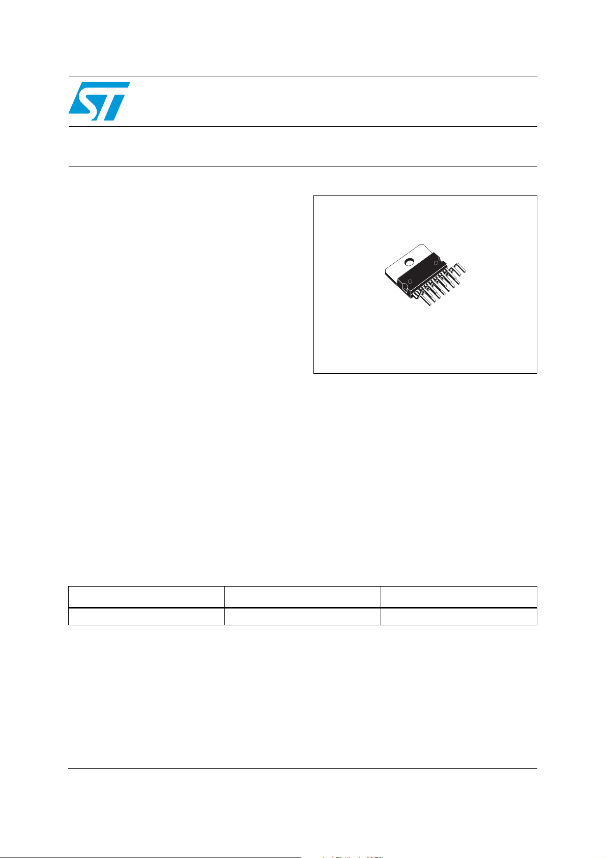
Table 1. Device summary
L4954
Multiwatt15
Description
L4954 is a quad output voltage regulator and a
three output high side driver.
The IC includes monitoring circuitry to warn the
microprocessor of a low voltage condition: the
LVWarn, output, sensing the slow dropping of
STCAP pins voltage, gives the microprocessor
time to store data.
A reset output is generated at REG4’s decay.
External protection must be provided for reverse
battery protection.
Order code Package Packing
L4954 Multiwatt15 Tube
July 2010 Doc ID 17719 Rev 1 1/13
www.st.com
1

Contents L4954
Contents
1 Block and pins connection diagrams . . . . . . . . . . . . . . . . . . . . . . . . . . . 5
2 Electrical specifications . . . . . . . . . . . . . . . . . . . . . . . . . . . . . . . . . . . . . . 6
2.1 Absolute maximum ratings . . . . . . . . . . . . . . . . . . . . . . . . . . . . . . . . . . . . . 6
2.2 Thermal data . . . . . . . . . . . . . . . . . . . . . . . . . . . . . . . . . . . . . . . . . . . . . . . 6
2.3 Application circuit . . . . . . . . . . . . . . . . . . . . . . . . . . . . . . . . . . . . . . . . . . . . 6
2.4 Electrical characteristics . . . . . . . . . . . . . . . . . . . . . . . . . . . . . . . . . . . . . . . 7
3 Functional description . . . . . . . . . . . . . . . . . . . . . . . . . . . . . . . . . . . . . . 10
4 Package information . . . . . . . . . . . . . . . . . . . . . . . . . . . . . . . . . . . . . . . . 11
5 Revision history . . . . . . . . . . . . . . . . . . . . . . . . . . . . . . . . . . . . . . . . . . . 12
2/13 Doc ID 17719 Rev 1

L4954 List of tables
List of tables
Table 1. Device summary . . . . . . . . . . . . . . . . . . . . . . . . . . . . . . . . . . . . . . . . . . . . . . . . . . . . . . . . . . 1
Table 2. Absolute maximum ratings . . . . . . . . . . . . . . . . . . . . . . . . . . . . . . . . . . . . . . . . . . . . . . . . . . 6
Table 3. Thermal data. . . . . . . . . . . . . . . . . . . . . . . . . . . . . . . . . . . . . . . . . . . . . . . . . . . . . . . . . . . . . 6
Table 4. Electrical characteristics . . . . . . . . . . . . . . . . . . . . . . . . . . . . . . . . . . . . . . . . . . . . . . . . . . . . 7
Table 5. Document revision history . . . . . . . . . . . . . . . . . . . . . . . . . . . . . . . . . . . . . . . . . . . . . . . . . 12
Doc ID 17719 Rev 1 3/13

List of figures L4954
List of figures
Figure 1. Block diagram . . . . . . . . . . . . . . . . . . . . . . . . . . . . . . . . . . . . . . . . . . . . . . . . . . . . . . . . . . . . 5
Figure 2. Pins connection diagram (top view) . . . . . . . . . . . . . . . . . . . . . . . . . . . . . . . . . . . . . . . . . . . 5
Figure 3. Application circuit . . . . . . . . . . . . . . . . . . . . . . . . . . . . . . . . . . . . . . . . . . . . . . . . . . . . . . . . . 6
Figure 4. Timing diagram . . . . . . . . . . . . . . . . . . . . . . . . . . . . . . . . . . . . . . . . . . . . . . . . . . . . . . . . . . 10
Figure 5. Multiwatt15 mechanical data and package dimensions . . . . . . . . . . . . . . . . . . . . . . . . . . . 11
4/13 Doc ID 17719 Rev 1

L4954 Block and pins connection diagrams
1 Block and pins connection diagrams
Figure 1. Block diagram
V
S
STCAP
REG1
10V, 40mA
10V-REG1
VOLTAGE
REFERENCE
CURRENT
LIMIT
RESET
LVWarn
EN1
EN2
EN3
GND
RESET
LVW
OUTPUT
CONTROL
THERMAL
SHUTDOWN
OVERVOLTAGE
PROTECTION
Figure 2. Pins connection diagram (top view)
15
14
13
12
11
10
9
8
7
6
5
4
3
2
1
REG2
8.5V, 175mA
REG3
5V, 650mA
REG4
5V, 100mA
HSD1
2.0A
HSD2
0.3A
HSD3
0.3A
8.5V-REG2
5V-REG3
5V-REG4-STBY
HSD1
HSD2
HSD3
D95AU346
10V REG1
8.5V REG2
5V REG3
EN3
EN2
EN1
RESET
GND
LVWarn
5V REG4-STBY
ST CAP
HSD3-0.3A
HSD2-0.3A
V
S
HSD1-2A
TAB CONNECTED TO PIN 8
Doc ID 17719 Rev 1 5/13
D95AU347

Electrical specifications L4954
(*)
2 Electrical specifications
2.1 Absolute maximum ratings
Table 2. Absolute maximum ratings
Symbol Parameter Value Unit
V
DC operating supply voltage -0.6 to 26.5 V
S
Transient supply overvoltages, rise time = 10 ms ,delay
V
S
time = 115 ms
34 V
V
V
T
Overvoltage shutdown 27 V
S,ovs
Input voltages (EN1, EN2, EN3) -0.6 to 6.0 V
V
in
Output voltages (LVWarn, RESET) -0.6 to 6.0 V
out
T
Operating temperature range -40 to 85 °C
op
Storage temperature range -40 to 150 °C
stg
2.2 Thermal data
Table 3. Thermal data
Symbol Parameter Value Unit
R
Thermal resistance junction-to-case 2 °C/W
th j-case
2.3 Application circuit
Figure 3. Application circuit
+V
S
1000μF 0.1μF
EN1
EN2
470μF
ESR of output capacitors should be between 0.2Ω to 5.0Ω
10
11
12EN3
1HSD1
3HSD2
4HSD3
5STCAP
2
L4954
8
15
14
13
6
7
9
6/13 Doc ID 17719 Rev 1
10μF(*)
10μF(*)
10μF(*)
10μF(*)
47KΩ 47KΩ
0.1μF
0.1μF
10V-REG1
8.5V-REG2
5V-REG3
5V-REG4
-STBY
LVWarn
RESET
D95AU348C

L4954 Electrical specifications
2.4 Electrical characteristics
Refer to the Figure 3: Application circuit, VS = 14.4 V; T
= 5 mA; I
OUT5
= 5 mA; I
OUT5 ST-BY
= 0.5 mA; R
HSD1
= 16 Ω, R
= 25 °C; I
amb
OUT10
= 107 Ω, unless
HSD2,3
= 5 mA; I
OUT8.5
otherwise specified.
Table 4. Electrical characteristics
Symbol Parameter Test condition Min. Typ. Max. Unit
V
S
Iq Maximum quiescent current
I
q,ST-BY
V
ENL
V
ENH
10 V / 40 mA reg 1 output
V
OUT10
ΔV
line
ΔV
load
V
DROPOUT
I
q1
I
lim1
SVR1 Reg 1 supply voltage rejection
8.5V / 175 mA reg 2 output
Operating supply voltage - 11 - 16 V
Standby quiescent current
EN1, EN2, EN3 input low
voltage
EN1, EN2, EN3 input high
voltage (outputs active)
Output voltage I
= 40 mA; I
I
OUT10
I
= 650 mA;
OUT5
I
OUT5ST-BY
R
HSD2,3
= 100mA; R
= 53 Ω
EN1, EN2, EN3 = 0
I
OUT5, ST-BY
= 50 mA
EN1, EN2, EN3 = 0
I
OUT5, ST-BY
= 2 mA
-0 -0.8 V
-2 -5 V
= 40 mA - 10 - V
OUT10
OUT8.5
= 175 mA;
= 8 Ω;
HSD1
- 10 - mA
-420 -mA
-300 -mA
Line regulation VS = 11 to 26 V - 2 - mV
Load regulation I
Dropout voltage
Reg 1 quiescent current
= 5 to 40 mA - 2 - mV
OUT10
V
= V
S
I
OUT10
= V
V
S
I
OUT10
I
OUT10
I
OUT10
+ 0.1 V
OUT10
= 5 mA
+ 0.5 V
OUT10
= 40 mA
- 100 200 mV
- 500 600 mV
= 5 mA - 7 - mA
= 40 mA - 7 - mA
Current limit - - 100 - mA
f = 0.12 to 10 kHz; I
mA; V
=1 Vpp
RIP
OUT10
= 25
- 55 - dB
V
OUT8.5
ΔV
line
ΔV
load
V
DROPOUT
Output voltage I
= 175 mA - 8.5 - V
OUT8.5
Line regulation VS = 11 to 26 V - 2 - mV
Load regulation I
Dropout voltage
= 5 to 175 mA - 10 - mV
OUT8.5
V
= V
S
I
OUT8.5
= V
V
S
I
OUT8.5
+ 0.3 V
OUT8.5
= 5 mA
+1 V
OUT8.5
= 175 mA
- 300 400 mV
- - 1.1 V
Doc ID 17719 Rev 1 7/13

Electrical specifications L4954
Table 4. Electrical characteristics (continued)
Symbol Parameter Test condition Min. Typ. Max. Unit
I
= 5 mA - 7 - mA
Iq2 Reg 2 quiescent current
I
lim2
Current limit - 300 - mA
5 V / 650 mA reg 3 output
V
Output voltage I
OUT5
ΔV
Line regulation VS = 7 to 26 V - 2 - mV
line
Load regulation I
ΔV
load
V
DROPOUT
Dropout voltage
I
Reg 3 quiescent current
q3
Current limit - - 1.25 - A
I
lim3
SVR3 Reg 3 supply voltage rejection
5V / 100 mA standby reg 4 output
OUT8.5
I
= 175 mA - 7 - mA
OUT8.5
= 650 mA - 5 - V
OUT5
= 5 to 650mA - 9 - mV
OUT5
= V
V
S
I
OUT5
= V
V
S
I
OUT5
I
OUT5
I
OUT5
f = 0.12 to 10 kHz;
I
OUT5
+ 0.3 V
OUT5
= 5 mA
+1 V
OUT5
= 650mA
- 300 400 mV
- 1 1.1 V
= 5 mA - 7 - mA
= 650 mA - 7 - mA
= 325 mA; V
=1 Vpp
RIP
- 55 - dB
V
OUT5STBY
ΔV
ΔV
V
DROPOUT
Output voltage I
Line regulation VS = 7 to 26 V - 0.8 - mV
line
Load regulation I
load
Dropout voltage
Reg 4 quiescent current
I
q4
I
Current limit - - 190 - mA
lim4
SVR4 Reg 4 supply voltage rejection
2 A HSD1
V
sat,peak
I
lim
I
leak1
I
Maximum output current
saturation voltage
Quiescent current - - 9 - mA
q
Current limit R
Output leakage current All driver outputs are off - 20 - mA
OUT5STBY
out
V
S
= 5mA
V
S
= 100 mA
I
OUT5STBY
I
OUT5STBY
f = 0.12 to 10 kHz
I
out5STBY
R
HSD1
HSD1
= 100 mA - 5 - V
= 0.5 to 100 mA - 3.5 - mV
= V
= V
REG5STBY
REG5STBY
+ 0.1 V I
+ 0.5 V I
out5STBY
out5STBY
- 100 200 mV
- 500 600 mV
= 2 mA - 0.25 - mA
= 100 mA - 0.35 - mA
= 50 mA; V
RIP
=1 Vpp
- 55 - dB
= 8 Ω -600 -mV
= 0.5 Ω -3.5 -A
8/13 Doc ID 17719 Rev 1
L4954 Electrical specifications
Table 4. Electrical characteristics (continued)
Symbol Parameter Test condition Min. Typ. Max. Unit
0.3 A HSD2 & HSD3
V
sat
I
I
lim
I
leak2,3
Maximum output current
saturation voltage
Quiescent current - - 1.5 - mA
q
Current limit R
Output leakage current All driver outputs are off - 10 - µA
SVR2 Reg 1supply voltage rejection
LVWARN OUTPUT
TH
V
LV W
t
rise
t
LV W
fall
LVW threshold on STCAP - - 7.5 - V
LVW output voltage
LVW output rise time
LVW output fall time - 12.6 - µs
Reset output
T
Reset threshold on reg 4 - - 4.5 - V
HRES
Reset output voltage
V
RES
R
= 53 Ω -150 -mV
HSD2,3
= 0.5 Ω -500 -mA
HSD2.3
f = 0.12 to 10 kHz;
= 100 mA; V
I
OUT8.5
STCAP < 7.5 V; V
STCAP > 7.5 V V
= 0.1 µF
C
LV W
Set VS so that V
=1Vpp
RIP
= ”0” 0 - 0.4 V
IL
= ”1” 2.75 - 5 V
IH
OUT5STBY
< 4.5 V;
VIL = ”0”
Set V
so that V
S
OUT5STBY
is not
less than normal reg 4 output
voltage; VIH = ”1”
- 55 - dB
-3.9 -ms
0 - 0.4 V
2.75 - 5 V
t
Reset output rise time
rise
t
fall
Reset output fall time - 37 - µs
C
RESET
=0.1 µF
Doc ID 17719 Rev 1 9/13
-4.5 -ms

Functional description L4954
3 Functional description
The L4954 includes a monitoring circuit to warn the microprocessor if a low voltage or no
voltage condition is occurring.
When the voltage on the STCAP pin drops below 7.5 V (typ), the LVW output goes low. This
tells the microprocessor to stop executing code and save vital information. The reset output
goes low when REG4 (5 V - standby) drops below (V
value. The RESET output doesn’t go above 0.4V until REG4 has gone back above 4.75 V
(min).
Any spike tells the microprocessor to start operating. Once the STCAP line passes 7.5 V
(typ), the LVWarn output also returns to high state.
The STCAP pin acts like a delay circuit. Due to the large capacitor (470 μF), the STCAP pin
allows the battery voltage to decay slowly giving the microprocessor time to store data.
Also, during short low voltage or negative voltage conditions, the STCAP pin protects the
5 V standby output from dropping below the RESET and LVW trip points. The four outputs
are expected to follow the battery voltage down to 11 V for REG1, 9 V for REG2, 6 V for
REG3 and REG4.
The L4954 has a standby mode to keep the microprocessor and memories alive during
ignition off conditions. The EN1 input pin is controlled by the microprocessor. A high on the
EN1 input turns on REG1, REG2, REG3, and HSD1. A Low on EN1 places the part in
stand-by mode with REG4 on. The high side driver outputs HSD2 and HSD3 are controlled
by EN2 and EN3 respectively: a low on the control input turns the corresponding high side
driver off.
-250 mV) or 4.75 V is minimum
REG4
Figure 4. Timing diagram
STCAP
(V)
0
5
REG4
(V)
0
5
LVWarn
(V)
5
RESET
(V)
0.4
7.5 7.5
4.75 4.75
D95AU349A
TIME
TIME
TIME
TIME
10/13 Doc ID 17719 Rev 1

L4954 Package information
4 Package information
In order to meet environmental requirements, ST offers these devices in different grades of
ECOPACK
®
packages, depending on their level of environmental compliance. ECOPACK
®
specifications, grade definitions and product status are available at: www.st.com.
ECOPACK
®
is an ST trademark.
Figure 5. Multiwatt15 mechanical data and package dimensions
DIM.
A5 0.197
B 2.65 0.104
C 1.6 0.063
D 1 0 .039
E 0.49 0.55 0.019 0.022
F 0.66 0.75 0.026 0.030
G 1.02 1.27 1.52 0.040 0.050 0.060
G1 17.53 17.78 18.03 0.690 0.700 0.710
H1 19.6 0.772
H2 20.2 0.795
L 21.9 22.2 22.5 0.862 0.874 0.886
L1 21.7 22.1 22.5 0.854 0.87 0.886
L2 17.65 18.1 0.695 0.7 13
L3 17.25 17.5 17.7 5 0.679 0.689 0.699
L4 10.3 10.7 10.9 0.406 0.421 0.429
L7 2.65 2.9 0.104 0.114
M 4.25 4.55 4.85 0.167 0.179 0.191
M1 4.73 5.08 5.43 0.186 0.200 0.214
S 1.9 2.6 0.075 0.102
S1 1.9 2.6 0.075 0.1 02
Dia1 3.65 3.85 0.144 0.152
mm inch
MIN. TYP. MAX. MIN. TYP. MAX.
OUTLINE AND
MECHANICAL DATA
Multiwatt15 (vertical)
0016036 J
Doc ID 17719 Rev 1 11/13

Revision history L4954
5 Revision history
Table 5. Document revision history
Date Revision Changes
12-Jul-2010 1 Initial release.
12/13 Doc ID 17719 Rev 1

L4954
Please Read Carefully:
Information in this document is provided solely in connection with ST products. STMicroelectronics NV and its subsidiaries (“ST”) reserve the
right to make changes, corrections, modifications or improvements, to this document, and the products and services described herein at any
time, without notice.
All ST products are sold pursuant to ST’s terms and conditions of sale.
Purchasers are solely responsible for the choice, selection and use of the ST products and services described herein, and ST assumes no
liability whatsoever relating to the choice, selection or use of the ST products and services described herein.
No license, express or implied, by estoppel or otherwise, to any intellectual property rights is granted under this document. If any part of this
document refers to any third party products or services it shall not be deemed a license grant by ST for the use of such third party products
or services, or any intellectual property contained therein or considered as a warranty covering the use in any manner whatsoever of such
third party products or services or any intellectual property contained therein.
UNLESS OTHERWISE SET FORTH IN ST’S TERMS AND CONDITIONS OF SALE ST DISCLAIMS ANY EXPRESS OR IMPLIED
WARRANTY WITH RESPECT TO THE USE AND/OR SALE OF ST PRODUCTS INCLUDING WITHOUT LIMITATION IMPLIED
WARRANTIES OF MERCHANTABILITY, FITNESS FOR A PARTICULAR PURPOSE (AND THEIR EQUIVALENTS UNDER THE LAWS
OF ANY JURISDICTION), OR INFRINGEMENT OF ANY PATENT, COPYRIGHT OR OTHER INTELLECTUAL PROPERTY RIGHT.
UNLESS EXPRESSLY APPROVED IN WRITING BY AN AUTHORIZED ST REPRESENTATIVE, ST PRODUCTS ARE NOT
RECOMMENDED, AUTHORIZED OR WARRANTED FOR USE IN MILITARY, AIR CRAFT, SPACE, LIFE SAVING, OR LIFE SUSTAINING
APPLICATIONS, NOR IN PRODUCTS OR SYSTEMS WHERE FAILURE OR MALFUNCTION MAY RESULT IN PERSONAL INJURY,
DEATH, OR SEVERE PROPERTY OR ENVIRONMENTAL DAMAGE. ST PRODUCTS WHICH ARE NOT SPECIFIED AS "AUTOMOTIVE
GRADE" MAY ONLY BE USED IN AUTOMOTIVE APPLICATIONS AT USER’S OWN RISK.
Resale of ST products with provisions different from the statements and/or technical features set forth in this document shall immediately void
any warranty granted by ST for the ST product or service described herein and shall not create or extend in any manner whatsoever, any
liability of ST.
ST and the ST logo are trademarks or registered trademarks of ST in various countries.
Information in this document supersedes and replaces all information previously supplied.
The ST logo is a registered trademark of STMicroelectronics. All other names are the property of their respective owners.
© 2010 STMicroelectronics - All rights reserved
STMicroelectronics group of companies
Australia - Belgium - Brazil - Canada - China - Czech Republic - Finland - France - Germany - Hong Kong - India - Israel - Italy - Japan -
Malaysia - Malta - Morocco - Philippines - Singapore - Spain - Sweden - Switzerland - United Kingdom - United States of America
www.st.com
Doc ID 17719 Rev 1 13/13
 Loading...