

Page 1
Features
■ ECOPACK
■ Automotive Grade: compliance with AEC
guidelines
■ Operating DC supply voltage range 5 V - 28 V
■ Transient supply voltage up to 40V
■ Extremely low quiescent current in standby
mode
■ High precision standby output voltage 5V±1%
■ Output current capability up to 100mA
■ Very low dropout voltage less than 0.5V
■ Reset circuit sensing the output voltage
■ Programmable reset pulse delay with external
capacitor
■ Voltage sense comparator
■ Thermal shutdown and short circuit protections
®
: lead free and RoHS compliant
L4949ED-E
L4949EP-E
Multifunction very low drop
voltage regulator
SO-8
SO-20W (12+4+4)
Description
The L4949ED-E and L4949EP-E are monolithic
integrated 5V voltage regulators with a very low
dropout output and additional functions as poweron reset and input voltage sense. They are
designed for supplying the microcomputer
controlled systems especially in automotive
applications.
Table 1. Device summary
Package
Tube Tape and reel
SO-8 L4949ED-E L4949EDTR-E
SO-20W L4949EP-E L4949EPTR-E
November 2009 Doc ID 16823 Rev 1 1/19
Order codes
www.st.com
1
Page 2

Contents L4949ED-E, L4949EP-E
Contents
1 Block diagram and pin description . . . . . . . . . . . . . . . . . . . . . . . . . . . . 5
2 Electrical specifications . . . . . . . . . . . . . . . . . . . . . . . . . . . . . . . . . . . . . . 7
2.1 Absolute maximum ratings . . . . . . . . . . . . . . . . . . . . . . . . . . . . . . . . . . . . . 7
2.2 Thermal data . . . . . . . . . . . . . . . . . . . . . . . . . . . . . . . . . . . . . . . . . . . . . . . 7
2.3 Electrical characteristics . . . . . . . . . . . . . . . . . . . . . . . . . . . . . . . . . . . . . . . 8
3 Application information . . . . . . . . . . . . . . . . . . . . . . . . . . . . . . . . . . . . . 10
3.1 Supply voltage transient . . . . . . . . . . . . . . . . . . . . . . . . . . . . . . . . . . . . . 10
3.2 Functional description . . . . . . . . . . . . . . . . . . . . . . . . . . . . . . . . . . . . . . . 10
3.3 Voltage regulator . . . . . . . . . . . . . . . . . . . . . . . . . . . . . . . . . . . . . . . . . . . 11
3.4 Preregulator . . . . . . . . . . . . . . . . . . . . . . . . . . . . . . . . . . . . . . . . . . . . . . . 12
3.5 Reset circuit . . . . . . . . . . . . . . . . . . . . . . . . . . . . . . . . . . . . . . . . . . . . . . . 13
3.6 Sense comparator . . . . . . . . . . . . . . . . . . . . . . . . . . . . . . . . . . . . . . . . . . 13
4 Package and packing information . . . . . . . . . . . . . . . . . . . . . . . . . . . . . 15
4.1 ECOPACK® packages . . . . . . . . . . . . . . . . . . . . . . . . . . . . . . . . . . . . . . . 15
4.2 SO-8 TP package information . . . . . . . . . . . . . . . . . . . . . . . . . . . . . . . . . 15
4.3 SO-20 TP package information . . . . . . . . . . . . . . . . . . . . . . . . . . . . . . . . 16
5 Revision history . . . . . . . . . . . . . . . . . . . . . . . . . . . . . . . . . . . . . . . . . . . 18
2/19 Doc ID 16823 Rev 1
Page 3

L4949ED-E, L4949EP-E List of tables
List of tables
Table 1. Device summary . . . . . . . . . . . . . . . . . . . . . . . . . . . . . . . . . . . . . . . . . . . . . . . . . . . . . . . . . . 1
Table 2. Pin definitions and functions . . . . . . . . . . . . . . . . . . . . . . . . . . . . . . . . . . . . . . . . . . . . . . . . . 6
Table 3. Absolute maximum ratings . . . . . . . . . . . . . . . . . . . . . . . . . . . . . . . . . . . . . . . . . . . . . . . . . . 7
Table 4. Thermal data. . . . . . . . . . . . . . . . . . . . . . . . . . . . . . . . . . . . . . . . . . . . . . . . . . . . . . . . . . . . . 7
Table 5. Electrical characteristics . . . . . . . . . . . . . . . . . . . . . . . . . . . . . . . . . . . . . . . . . . . . . . . . . . . . 8
Table 6. Reset . . . . . . . . . . . . . . . . . . . . . . . . . . . . . . . . . . . . . . . . . . . . . . . . . . . . . . . . . . . . . . . . . . 8
Table 7. Sense . . . . . . . . . . . . . . . . . . . . . . . . . . . . . . . . . . . . . . . . . . . . . . . . . . . . . . . . . . . . . . . . . . 9
Table 8. Preregulator . . . . . . . . . . . . . . . . . . . . . . . . . . . . . . . . . . . . . . . . . . . . . . . . . . . . . . . . . . . . . 9
Table 9. SO-8 TP mechanical data. . . . . . . . . . . . . . . . . . . . . . . . . . . . . . . . . . . . . . . . . . . . . . . . . . 15
Table 10. SO-20 TP mechanical data. . . . . . . . . . . . . . . . . . . . . . . . . . . . . . . . . . . . . . . . . . . . . . . . . 16
Table 11. Document revision history . . . . . . . . . . . . . . . . . . . . . . . . . . . . . . . . . . . . . . . . . . . . . . . . . 18
Doc ID 16823 Rev 1 3/19
Page 4

List of figures L4949ED-E, L4949EP-E
List of figures
Figure 1. Block diagram . . . . . . . . . . . . . . . . . . . . . . . . . . . . . . . . . . . . . . . . . . . . . . . . . . . . . . . . . . . . 5
Figure 2. Configuration diagram (top view) . . . . . . . . . . . . . . . . . . . . . . . . . . . . . . . . . . . . . . . . . . . . . 5
Figure 3. Application circuit
Figure 4. Foldback characteristic of V
Figure 5. Output voltage vs input voltage . . . . . . . . . . . . . . . . . . . . . . . . . . . . . . . . . . . . . . . . . . . . . 12
Figure 6. Quiescent current vs supply voltage. . . . . . . . . . . . . . . . . . . . . . . . . . . . . . . . . . . . . . . . . . 12
Figure 7. Block circuit of reset circuit . . . . . . . . . . . . . . . . . . . . . . . . . . . . . . . . . . . . . . . . . . . . . . . . . 13
Figure 8. Waveforms . . . . . . . . . . . . . . . . . . . . . . . . . . . . . . . . . . . . . . . . . . . . . . . . . . . . . . . . . . . . . 14
Figure 9. SO-8 TP package dimensions . . . . . . . . . . . . . . . . . . . . . . . . . . . . . . . . . . . . . . . . . . . . . . 16
Figure 10. SO20 TP package dimensions . . . . . . . . . . . . . . . . . . . . . . . . . . . . . . . . . . . . . . . . . . . . . . 17
(1)
. . . . . . . . . . . . . . . . . . . . . . . . . . . . . . . . . . . . . . . . . . . . . . . . . . . . . . 10
. . . . . . . . . . . . . . . . . . . . . . . . . . . . . . . . . . . . . . . . . . . . . . . 11
O
4/19 Doc ID 16823 Rev 1
Page 5
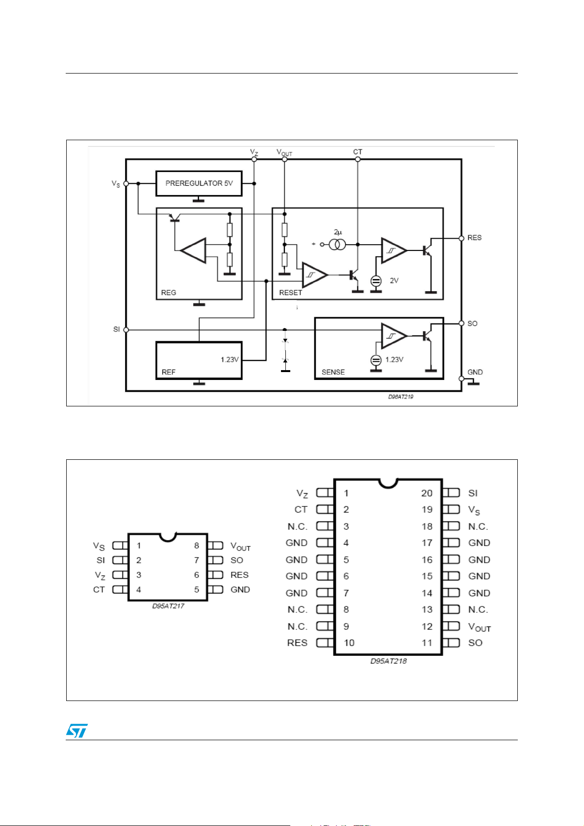
L4949ED-E, L4949EP-E Block diagram and pin description
1 Block diagram and pin description
Figure 1. Block diagram
Note: The block diagram illustrates only a major internal device functionality and it is not intended
to mimic any details of hardware design
Figure 2. Configuration diagram (top view)
SO-8
SO-20
Doc ID 16823 Rev 1 5/19
Page 6
Block diagram and pin description L4949ED-E, L4949EP-E
Table 2. Pin definitions and functions
Pin N°
Symbol Function
SO-8 SO-20
119 V
220 S
31 V
42 C
4, 5, 6, 7, 14,
5
15, 16, 17
S
I
Z
T
GND Ground reference
610 RES
Input supply voltage. Block to GND via an external
capacitor (see Figure 3).
Sense input pin to supervise input voltage. Connect via an
external voltage divider connected to V
Preregulator output voltage. For details, see Section 3.4:
Preregulator.
Reset pulse delay adjustment. Connecting this pin via a
capacitor to GND
Reset output. It is pulled down when the output voltage
goes below V
RT
.
Sense output. This open collector pin must be connected to
V
711 S
812 V
O
OUT
via an external resistor. It is pulled down whenever
OUT
voltage becomes lower than an internal voltage.
the S
I
Output voltage. Block to GND via an external capacitor (see
Figure 3)
- 3, 8, 9, 13, 18 NC Not connected pins
and to GND.
S
6/19 Doc ID 16823 Rev 1
Page 7
L4949ED-E, L4949EP-E Electrical specifications
2 Electrical specifications
2.1 Absolute maximum ratings
Table 3. Absolute maximum ratings
Symbol Parameter Value Unit
V
DC operating supply voltage 28 V
SDC
Transient supply voltage (T < 1s) 40 V
V
STR
Output current Internally limited
I
O
V
Output voltage 20 V
O
, VSO Output voltage 20 V
V
RES
, ISO Output current 5 mA
I
RES
V
V
SIDC
V
I
T
T
1.
The circuit is ESD protected according to MIL-STD-883C.
Reset delay voltage 7 V
CT
Sense input voltage 28 V
Preregulator output voltage 7 V
Z
Preregulator output current 5 mA
Z
Junction temperature -40 to +150 °C
J
Storage temperature range -55 to +150 °C
stg
2.2 Thermal data
(1)
Table 4. Thermal data
Symbol Description SO-8 SO20L Unit
R
R
Thermal Resistance Junction-ambient (max) 200 50 °C/W
th j-amb
th j-pins
Thermal Resistance Junction-pins (max) 15 °C/W
TJSD Thermal Shutdown Junction temperature 165 °C
Doc ID 16823 Rev 1 7/19
Page 8

Electrical specifications L4949ED-E, L4949EP-E
2.3 Electrical characteristics
VS = 14 V; -40 °C < Tj < 125 °C unless otherwise specified
Table 5. Electrical characteristics
Symbol Parameter Test condition Min. Typ. Max. Unit
V
O
V
O
V
O
V
DP
V
IO
I
outh
V
OL
V
OLO
I
LIM
I
QSE
I
Q
1. With this test we guarantee that with no output current the output voltage will not exceed 5.5V
2. Foldback characteristic
Output voltage TJ = 25 °C; IO = 1 mA 4.95 5 5.05 V
Output voltage 6 V < VIN < 28 V, 1 mA < IO < 50 mA 4.90 5 5.10 V
V
= 40 V;
Output voltage
Dropout voltage
IN
T < 1s; 5mA < IO < 100 mA
I
= 10 mA
O
= 50 mA
I
O
IO = 100 mA
4.75 5.25 V
0.1
0.2
0.3
0.25
0.4
0.5
V
V
V
Input to output voltage
difference in undervoltage
VIN = 4 V, IO = 35 mA 0.4 V
condition
(1)
Max output leakage VIN = 25 V, VO = 5.5 V 20 50 80 µA
Line regulation 6 V < VIN < 28 V; IO = 1 mA 20 mV
Load regulation 1 mA < IO < 100 mA 30 mV
200
100
400
400 mAmA
mA
Current limit
V
= 4.5 V
O
= 4.5 V; TJ = 25 °C
V
O
VO = 0 V
(2)
105
120
Quiescent current IO = 0.3 mA; TJ < 100 °C 200 300 µA
Quiescent current IO = 100 mA 5 mA
Table 6. Reset
Symbol Parameter Test condition Min. Typ. Max. Unit
V
Reset threshold voltage
RT
Reset threshold hysteresis 50 100 200 mV
V
RTH
Reset pulse delay CT = 100 nF; TR ≥ 100 µs 55 100 180 ms
t
RD
V
Reset output low voltage R
RL
IRH
V
CTth
V
CTth, hy
Reset output high leakage
current
Delay comparator threshold 2 V
Delay comparator threshold
hysteresis
= 10 KΩ to VO VS ≥ 1.5V 0.4 V
RES
V
= 5 V 1 µA
RES
VO -
0.5V
V
100 mV
8/19 Doc ID 16823 Rev 1
Page 9

L4949ED-E, L4949EP-E Electrical specifications
Table 7. Sense
Symbol Parameter Test condition Min. Typ. Max. Unit
V
Sense low threshold 1.16 1.23 1.35 V
st
Sense threshold hysteresis 20 100 200 mV
V
sth
≤ 1.16 V; VS ≥ 3V
V
VSL Sense output low voltage
Sense output leakage VSO = 5 V; VSI ≥ 1.5 V 1 µA
I
SH
Sense input current VSI = 0 -20 -8 -3 µA
I
SI
Table 8. Preregulator
SI
= 10 KΩ to VO
R
SO
0.4 V
Symbol Parameter Test condition Min. Typ. Max. Unit
V
I
Z
Preregulator output voltage IZ = 10 µA 4.5 5 6 V
Z
Preregulator output current 10 µA
Doc ID 16823 Rev 1 9/19
Page 10

Application information L4949ED-E, L4949EP-E
3 Application information
Figure 3. Application circuit
(1)
1. For stability: C
≥ 1µF, CO ≥ 4.7µF, ESR < 10Ω at 10KHz. Recommended for application: CS = CO = 10 µF to 100 µF
S
3.1 Supply voltage transient
High supply voltage transients can cause a reset output signal disturbance. For supply
voltages greater than 8V the circuit shows a high immunity of the reset output against supply
transients of more than 100V/µs. For supply voltages less than 8V supply transients of more
than 0.4V/µs can cause a reset signal disturbance.
To improve the transient behaviour for supply voltages less than 8V a capacitor at pin V
be used.
This capacitor (C3 ≤ 1 µF) reduces also the output noise.
3.2 Functional description
The L4949ED-E and L4949EP-E are monolithic integrated voltage regulator, based on the
STM modular voltage regulator approach. Several outstanding features and auxiliary
functions are implemented to meet the requirements of supplying microprocessor systems
in automotive applications. Nevertheless, it is suitable also in other applications where the
can
Z
10/19 Doc ID 16823 Rev 1
Page 11
L4949ED-E, L4949EP-E Application information
present functions are required. The modular approach of this device allows to get easily also
other features and functions when required.
3.3 Voltage regulator
The voltage regulator uses an Isolated Collector Vertical PNP transistor as a regulating
element.
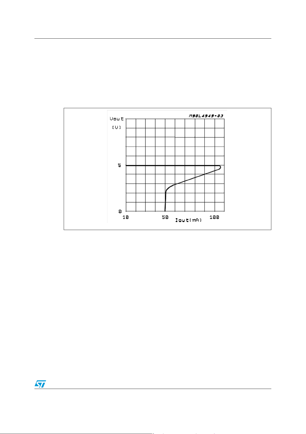
Figure 4. Foldback characteristic of V
With this structure very low dropout voltage at currents up to 100mA is obtained. The
dropout operation of the standby regulator is maintained down to 3V input supply voltage.
The output voltage is regulated up to the transient input supply voltage of 40V. With this
feature no functional interruption due to overvoltage pulses is generated. The typical curve
showing the standby output voltage as a function of the input supply voltage is shown in
Figure 5. The current consumption of the device (quiescent current) is less than 300 µA.
O
To reduce the quiescent current peak in the undervoltage region and to improve the
transient response in this region, the dropout voltage is controlled, the quiescent current as
a function of the supply input voltage is shown in Figure 6.
Doc ID 16823 Rev 1 11/19
Page 12

Application information L4949ED-E, L4949EP-E
Figure 5. Output voltage vs input voltage
Figure 6. Quiescent current vs supply voltage
3.4 Preregulator
To improve the transient immunity a preregulator stabilizes the internal supply voltage to 5 V.
This internal voltage is present at Pin 3 (V
because the output capability is very small (≤ 10 µA).
This output may be used as an option when a better transient behaviour for supply voltages
less than 8 V is required (see also application note).
In this case a capacitor (100 nF - 1 µF) must be connected between pin V
feature is not used pin V
12/19 Doc ID 16823 Rev 1
must be left open.
Z
). This voltage should not be used as an output
Z
and GND. If this
Z
Page 13

L4949ED-E, L4949EP-E Application information
3.5 Reset circuit
The block circuit diagram of the reset circuit is shown in Figure 7. The reset circuit
supervises the output voltage.
The reset threshold of 4.5 V is defined with the internal reference voltage and standby
output divider.
The reset pulse delay time t
t
RD
CT2V•
-------------------- -=
2μ A
The reaction time of the reset circuit originates from the discharge time limitation of the reset
capacitor CT and is proportional to the value of CT.
The reaction time of the reset circuit increases the noise immunity. Standby output voltage
drops below the reset threshold only a bit longer than the reaction time results in a shorter
reset delay time.
The nominal reset delay time is generated for standby output voltage drops longer than
approximately 50ms.
The typical reset output waveforms are shown in Figure 8.
, is defined with the charge time of an external capacitor CT:
RD
3.6 Sense comparator
The sense comparator compares an input signal with an internal voltage reference of typical
1.23V. The use of an external voltage divider makes this comparator very flexible in the
application.
It can be used to supervise the input voltage either before or after the protection diode and
to give additional informations to the microprocessor like low voltage warnings.
Figure 7. Block circuit of reset circuit
Doc ID 16823 Rev 1 13/19
Page 14

Application information L4949ED-E, L4949EP-E
Figure 8. Waveforms
14/19 Doc ID 16823 Rev 1
Page 15
L4949ED-E, L4949EP-E Package and packing information
4 Package and packing information
4.1 ECOPACK® packages
In order to meet environmental requirements, ST offers these devices in different grades of
ECOPACK
®
packages, depending on their level of environmental compliance. ECOPACK®
specifications, grade definitions and product status are available at: www.st.com
ECOPACK
®
is an ST trademark.
4.2 SO-8 TP package information
Table 9. SO-8 TP mechanical data
Dim.
Min. Typ. Max.
A 1.75
a1 0.1 0.25
a2 1.65
a3 0.65 0.85
b 0.35 0.48
b1 0.19 0.25
C 0.25 0.5
c1 45° (typ.)
(1)
D
E 5.8 6.2
4.8 5.0
.
mm
e 1.27
e3 3.81
(1)
F
L 0.4 1.27
M 0.6
S 8° (max.)
1. D and F do not include mold flash or protrusions. Mold flash or protrusions shall not exceed 0.15mm
(.006inch).
3.8 4.0
Doc ID 16823 Rev 1 15/19
Page 16

Package and packing information L4949ED-E, L4949EP-E
Figure 9. SO-8 TP package dimensions
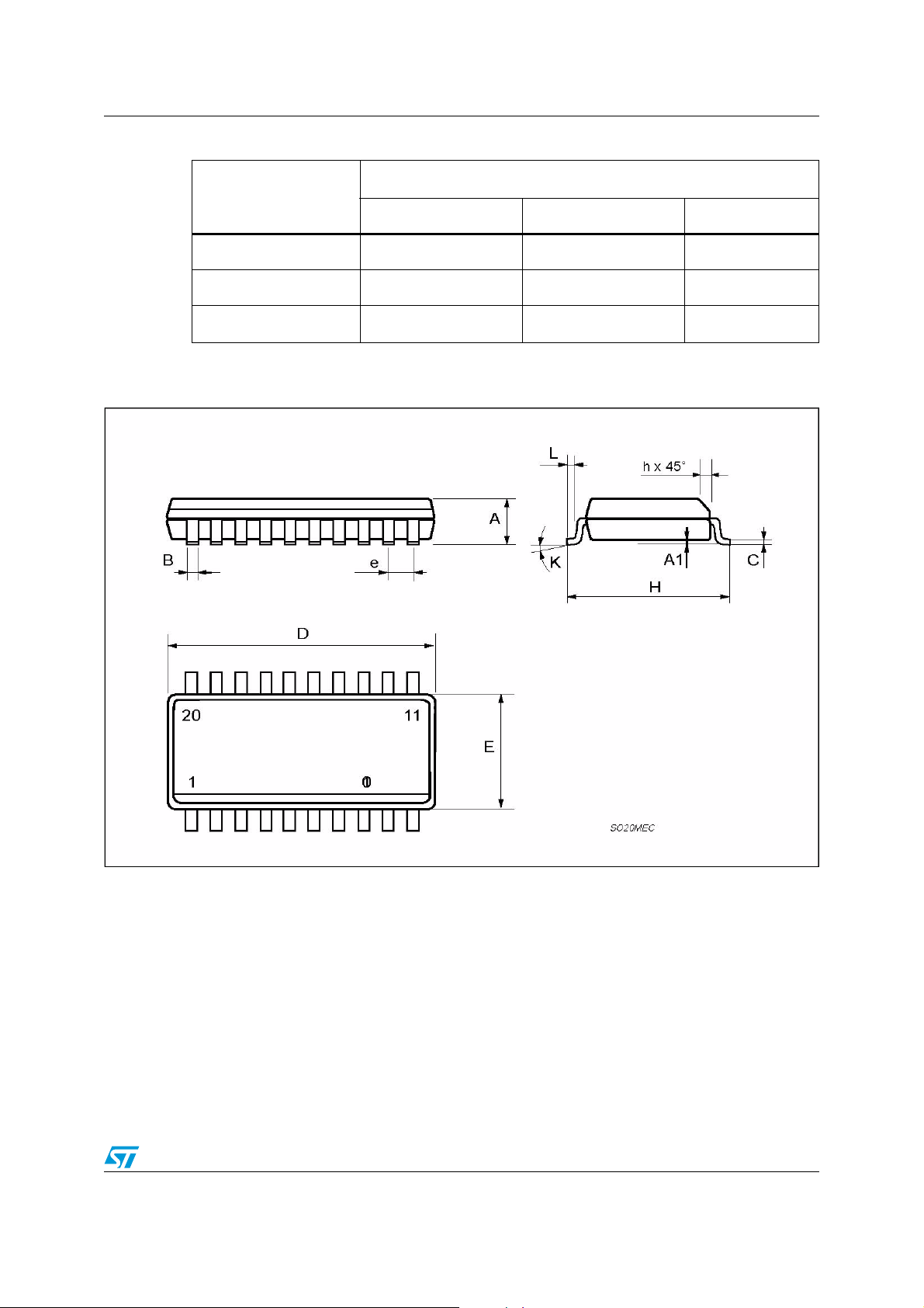
4.3 SO-20 TP package information
Table 10. SO-20 TP mechanical data
Dim.
Min. Typ. Max.
A 2.35 2.65
A1 0.1 0.3
B 0.33 0.51
C 0.23 0.32
D 12.6 13
E 7.4 7.6
e 1.27
H 10 10.65
mm
16/19 Doc ID 16823 Rev 1
Page 17
L4949ED-E, L4949EP-E Package and packing information
Table 10. SO-20 TP mechanical data (continued)
mm
Dim.
Min. Typ. Max.
h 0.25 0.75
L 0.4 1.27
K 0 (min.)8 (max.)
Figure 10. SO20 TP package dimensions
Doc ID 16823 Rev 1 17/19
Page 18

Revision history L4949ED-E, L4949EP-E
5 Revision history
Table 11. Document revision history
Date Revision Description of changes
24-Nov-2009 1 Initial release.
18/19 Doc ID 16823 Rev 1
Page 19

L4949ED-E, L4949EP-E
Please Read Carefully:
Information in this document is provided solely in connection with ST products. STMicroelectronics NV and its subsidiaries (“ST”) reserve the
right to make changes, corrections, modifications or improvements, to this document, and the products and services described herein at any
time, without notice.
All ST products are sold pursuant to ST’s terms and conditions of sale.
Purchasers are solely responsible for the choice, selection and use of the ST products and services described herein, and ST assumes no
liability whatsoever relating to the choice, selection or use of the ST products and services described herein.
No license, express or implied, by estoppel or otherwise, to any intellectual property rights is granted under this document. If any part of this
document refers to any third party products or services it shall not be deemed a license grant by ST for the use of such third party products
or services, or any intellectual property contained therein or considered as a warranty covering the use in any manner whatsoever of such
third party products or services or any intellectual property contained therein.
UNLESS OTHERWISE SET FORTH IN ST’S TERMS AND CONDITIONS OF SALE ST DISCLAIMS ANY EXPRESS OR IMPLIED
WARRANTY WITH RESPECT TO THE USE AND/OR SALE OF ST PRODUCTS INCLUDING WITHOUT LIMITATION IMPLIED
WARRANTIES OF MERCHANTABILITY, FITNESS FOR A PARTICULAR PURPOSE (AND THEIR EQUIVALENTS UNDER THE LAWS
OF ANY JURISDICTION), OR INFRINGEMENT OF ANY PATENT, COPYRIGHT OR OTHER INTELLECTUAL PROPERTY RIGHT.
UNLESS EXPRESSLY APPROVED IN WRITING BY AN AUTHORIZED ST REPRESENTATIVE, ST PRODUCTS ARE NOT
RECOMMENDED, AUTHORIZED OR WARRANTED FOR USE IN MILITARY, AIR CRAFT, SPACE, LIFE SAVING, OR LIFE SUSTAINING
APPLICATIONS, NOR IN PRODUCTS OR SYSTEMS WHERE FAILURE OR MALFUNCTION MAY RESULT IN PERSONAL INJURY,
DEATH, OR SEVERE PROPERTY OR ENVIRONMENTAL DAMAGE. ST PRODUCTS WHICH ARE NOT SPECIFIED AS "AUTOMOTIVE
GRADE" MAY ONLY BE USED IN AUTOMOTIVE APPLICATIONS AT USER’S OWN RISK.
Resale of ST products with provisions different from the statements and/or technical features set forth in this document shall immediately void
any warranty granted by ST for the ST product or service described herein and shall not create or extend in any manner whatsoever, any
liability of ST.
ST and the ST logo are trademarks or registered trademarks of ST in various countries.
Information in this document supersedes and replaces all information previously supplied.
The ST logo is a registered trademark of STMicroelectronics. All other names are the property of their respective owners.
© 2009 STMicroelectronics - All rights reserved
STMicroelectronics group of companies
Australia - Belgium - Brazil - Canada - China - Czech Republic - Finland - France - Germany - Hong Kong - India - Israel - Italy - Japan -
Malaysia - Malta - Morocco - Philippines - Singapore - Spain - Sweden - Switzerland - United Kingdom - United States of America
www.st.com
Doc ID 16823 Rev 1 19/19
 Loading...