

Feature summary
■ Low dropout voltage (450mV typ. at 1A)
■ Very low quiescent current
■ Thermal shutdown
■ Short circuit protection
■ Reverse polarity protection
L4941
Very low drop 1A regulator
Description
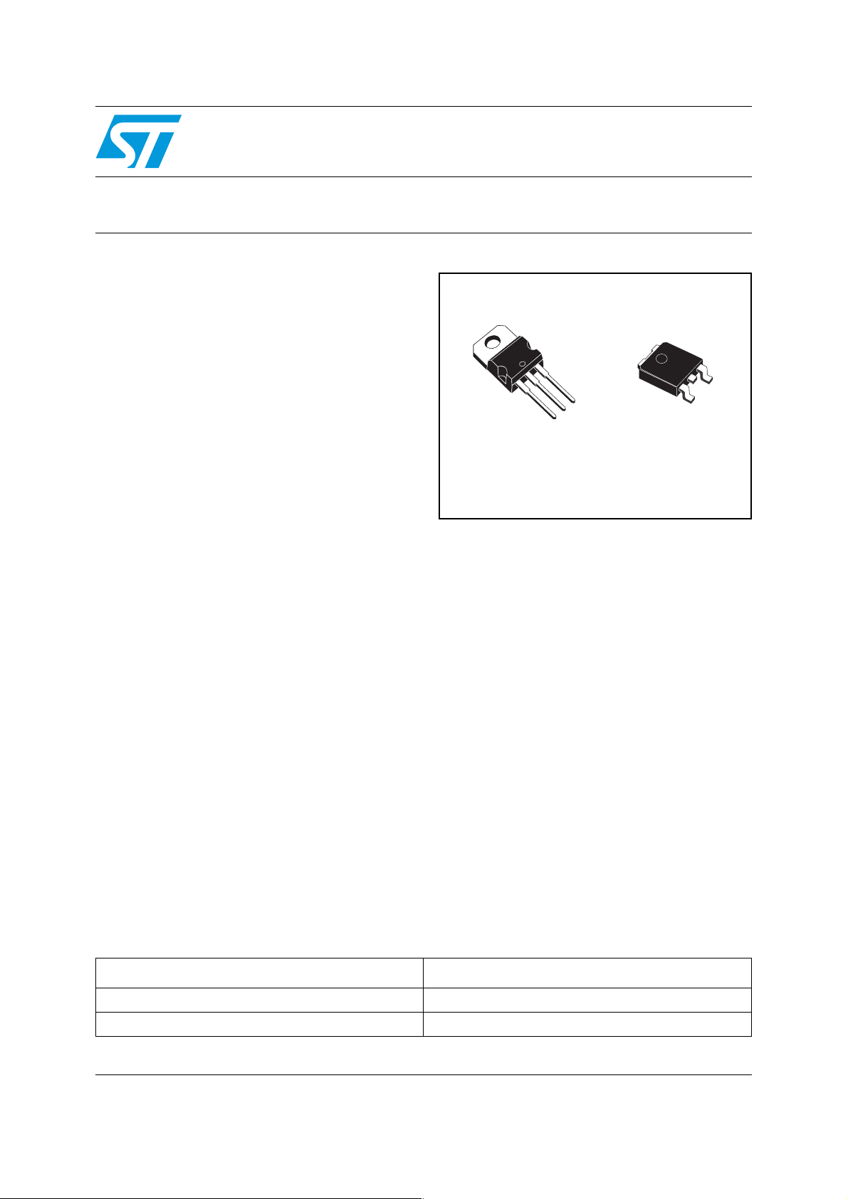
The L4941 is a three terminal 5V positive
regulators available in TO-220 and DPAK
packages, making it useful in a wide range of
industrial and consumer applications. Thanks to
its very low input/output voltage drop, these
devices are particularly suitable for battery
powered equipments, reducing consumption and
TO-220
prolonging battery life. It employs internal current
limiting, antisaturation circuit, thermal shut-down
and safe area protection.
DPAK
Order code
Part number Package
L4941BV TO-220
L4941BDT-TR DPAK
September 2006 Rev. 5 1/17
www.st.com
17

L4941
Contents
1 Block diagram . . . . . . . . . . . . . . . . . . . . . . . . . . . . . . . . . . . . . . . . . . . . . . 3
2 Pin configuration . . . . . . . . . . . . . . . . . . . . . . . . . . . . . . . . . . . . . . . . . . . 4
3 Maximum ratings . . . . . . . . . . . . . . . . . . . . . . . . . . . . . . . . . . . . . . . . . . . . 5
4 Test circuits . . . . . . . . . . . . . . . . . . . . . . . . . . . . . . . . . . . . . . . . . . . . . . . 6
5 Electrical characteristics . . . . . . . . . . . . . . . . . . . . . . . . . . . . . . . . . . . . . 7
6 Typical application . . . . . . . . . . . . . . . . . . . . . . . . . . . . . . . . . . . . . . . . . . 8
7 Schematic application . . . . . . . . . . . . . . . . . . . . . . . . . . . . . . . . . . . . . . 11
8 Package mechanical data . . . . . . . . . . . . . . . . . . . . . . . . . . . . . . . . . . . . 12
9 Revision history . . . . . . . . . . . . . . . . . . . . . . . . . . . . . . . . . . . . . . . . . . . 16
2/17

L4941 Block diagram
1 Block diagram
Figure 1. Block diagram
3/17
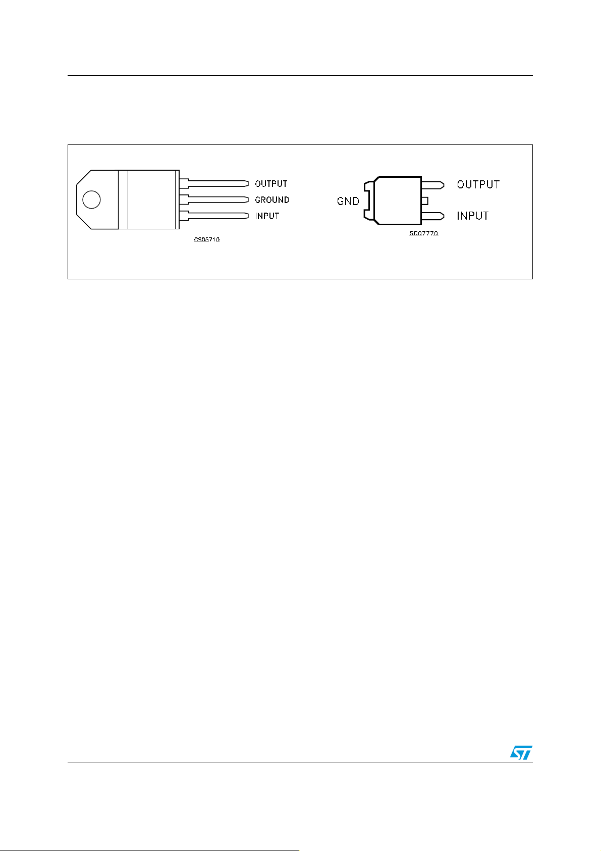
Pin configuration L4941
2 Pin configuration
Figure 2. Pin connections (top view)
TO-220
DPAK
4/17
L4941 Maximum ratings
3 Maximum ratings
Table 1. Absolute maximum ratings
Symbol Parameter Value Unit
V
I
V
IR
I
O
P
D
T
stg
T
op
Forward input voltage 30 V
Reverse input voltage (RO=100Ω)-15V
Output current Internally Limited mA
Power dissipation Internally Limited mW
Storage temperature range -40 to +150 °C
Operating junction temperature range -40 to +150 °C
Note: Absolute Maximum Ratings are those values beyond which damage to the device may
occur. Functional operation under these condition is not implied
Table 2. Thermal Data
Symbol Parameter TO-220 DPAK Unit
R
R
thJC
thJA
Thermal resistance junction-case 3 8 °C/W
Thermal resistance junction-ambient 50 100 °C/W
5/17

Test circuits L4941
4 Test circuits
Figure 3. DC Parameters
Figure 4. Load rejection
Figure 5. Ripple rejection
6/17

L4941 Electrical characteristics
5 Electrical characteristics
Table 3. Electrical characteristics (refer to test circuit, VI=7V, CI = 0.1µF, CO = 22µF, TJ = 25°C,
unless otherwise specified.)
Symbol Parameter Test conditions Min. Typ. Max. Unit
Output voltage IO = 5mA to 1A, VI = 6 to 14V 4.8 5 5.2 V
O
Input voltage IO = 5 mA 16 V
I
Line regulation VI = 6 to 16V, IO = 5 mA 5 20 mV
O
I
= 5mA to 1A 8 20 mV
Load regulation
O
Quiescent current
q
Quiescent current change
q
Dropout voltage
d
O
I
= 0.5A to 1A 5 15 mV
O
= 5 mA, VI = 6V 4 8 mA
I
O
I
= 1A, VI = 6V 20 40 mA
O
I
= 5 mA, VI = 6 to 14V 3 mA
O
I
= 1A, VI = 6 to 14V -10 mA
O
I
= 0.5A 250 450 mV
O
I
= 1A 450 700 mV
O
/∆T Output voltage drift 0.6 mV/°C
∆V
V
V
∆V
∆V
I
∆I
V
O
SVR Supply voltage rejection f = 120Hz, IO = 1A 58 68 dB
V
= 14V 1.6 2.0
I
sc
Z
e
Short circuit current
Output impedance f = 1KHz, IO = 0.5A 30 mΩ
O
Output noise voltage B = 100Hz to 100KHz 30 µV/V
N
I
= 6V 1.8 2.2
V
I
A
O
7/17

Typical application L4941
6 Typical application
Figure 6. Dropout voltage vs output current Figure 7. Dropout voltage vs temperature
Figure 8. Output voltage vs temperature Figure 9. Quiescent current vs temperature
Figure 10. Quiescent current vs input voltage Figure 11. Quiescent current vs output current
8/17

L4941 Typical application
Figure 12. Short circuit current vs temperature Figure 13. Peak output current vs input/output
differential voltage
Figure 14. Low voltage behavior Figure 15. Supply voltage rejection vs
frequency
Figure 16. Supply voltage rejection vs output
current
Figure 17. Load dump characteristics
9/17

Typical application L4941
Figure 18. Line transient response Figure 19. Total power dissipation
Figure 20. Load transient response
10/17

L4941 Schematic application
7 Schematic application
Figure 21. Distributed supply with On-card L4940 and L4941 low drop regulator
Figure 22. Distributed Supply with On-card L4940 and L4941 low drop regulator
ADVANTAGES OF THESE APPLICATION ARE:
On card regulation with short-circuit and thermal protection on each output.
Vary high total system efficiency due to the switching preregulation and very low-drop postregulation.
11/17

Package mechanical data L4941
8 Package mechanical data
In order to meet environmental requirements, ST offers these devices in ECOPACK®
packages. These packages have a Lead-free second level interconnect. The category of
second Level Interconnect is marked on the package and on the inner box label, in
compliance with JEDEC Standard JESD97. The maximum ratings related to soldering
conditions are also marked on the inner box label. ECOPACK is an ST trademark.
ECOPACK specifications are available at: www.st.com.
12/17

L4941 Package mechanical data
TO-220 MECHANICAL DAT
DIM.
A 4.40 4.60 0.173 0.181
C 1.23 1.32 0.048 0.051
D 2.40 2.72 0.094 0.107
D1 1.27 0.050
E 0.49 0.70 0.019 0.027
F 0.61 0.88 0.024 0.034
F1 1.14 1.70 0.044 0.067
F2 1.14 1.70 0.044 0.067
G 4.95 5.15 0.194 0.203
G1 2.4 2.7 0.094 0.106
H2 10.0 10.40 0.393 0.409
L2 16.4 0.645
L4 13.0 14.0 0.511 0.551
L5 2.65 2.95 0.104 0.116
L6 15.25 15.75 0.600 0.620
L7 6.2 6.6 0.244 0.260
L9 3.5 3.93 0.137 0.154
DIA. 3.75 3.85 0.147 0.151
MIN. TYP MAX. MIN. TYP. MAX.
mm. inch
A
P011C
13/17

Package mechanical data L4941
DPAK MECHANICAL DATA
DIM.
MIN. TY P MAX. MIN. TYP. MAX.
A 2.2 2.4 0.086 0.094
A1 0.9 1.1 0.035 0.043
A2 0.03 0.23 0.001 0.009
B 0.64 0.9 0.025 0.035
b4 5.2 5.4 0.204 0.212
C 0.45 0.6 0.017 0.023
C2 0.48 0.6 0.019 0.023
D 6 6.2 0.236 0.244
D1 5.1 0.200
E 6.4 6.6 0.252 0.260
E1 4.7 0.185
e 2.28 0.090
e1 4.4 4.6 0.173 0.181
H 9.35 10.1 0.368 0.397
L 1 0.039
(L1) 2.8 0.110
L2 0.8 0.031
L4 0.6 1 0.023 0.039
R 0.2 0.008
V2 0° 8° 0° 8°
mm. inch
14/17
0068772-F

L4941 Package mechanical data
Tape & Reel DPAK-PPAK MECHANICAL DATA
DIM.
MIN. TYP MAX. MIN. TYP. MAX.
A 330 12.992
C 12.8 13.0 13.2 0.504 0.512 0.519
D 20.2 0.795
N 60 2.362
T 22.4 0.882
Ao 6.80 6.90 7.00 0.268 0.272 0.2.76
Bo 10.40 10.50 10.60 0.409 0.413 0.417
Ko 2.55 2.65 2.75 0.100 0.104 0.105
Po 3.9 4.0 4.1 0.153 0.157 0.161
P 7.9 8.0 8.1 0.311 0.315 0.319
mm. inch
15/17

Revision history L4941
9 Revision history
Table 4. Revision history
Date Revision Changes
21-Jun-2004 4 Document updating.
15-Sep-2006 5 Order Codes has been updated and new template.
16/17

L4941
Please Read Carefully:
Information in this document is provided solely in connection with ST products. STMicroelectronics NV and its subsidiaries (“ST”) reserve the
right to make changes, corrections, modifications or improvements, to this document, and the products and services described herein at any
time, without notice.
All ST products are sold pursuant to ST’s terms and conditions of sale.
Purchasers are solely responsible for the choice, selection and use of the ST products and services described herein, and ST assumes no
liability whatsoever relating to the choice, selection or use of the ST products and services described herein.
No license, express or implied, by estoppel or otherwise, to any intellectual property rights is granted under this document. If any part of this
document refers to any third party products or services it shall not be deemed a license grant by ST for the use of such third party products
or services, or any intellectual property contained therein or considered as a warranty covering the use in any manner whatsoever of such
third party products or services or any intellectual property contained therein.
UNLESS OTHERWISE SET FORTH IN ST’S TERMS AND CONDITIONS OF SALE ST DISCLAIMS ANY EXPRESS OR IMPLIED
WARRANTY WITH RESPECT TO THE USE AND/OR SALE OF ST PRODUCTS INCLUDING WITHOUT LIMITATION IMPLIED
WARRANTIES OF MERCHANTABILITY, FITNESS FOR A PARTICULAR PURPOSE (AND THEIR EQUIVALENTS UNDER THE LAWS
OF ANY JURISDICTION), OR INFRINGEMENT OF ANY PATENT, COPYRIGHT OR OTHER INTELLECTUAL PROPERTY RIGHT.
UNLESS EXPRESSLY APPROVED IN WRITING BY AN AUTHORIZED ST REPRESENTATIVE, ST PRODUCTS ARE NOT
RECOMMENDED, AUTHORIZED OR WARRANTED FOR USE IN MILITARY, AIR CRAFT, SPACE, LIFE SAVING, OR LIFE SUSTAINING
APPLICATIONS, NOR IN PRODUCTS OR SYSTEMS WHERE FAILURE OR MALFUNCTION MAY RESULT IN PERSONAL INJURY,
DEATH, OR SEVERE PROPERTY OR ENVIRONMENTAL DAMAGE. ST PRODUCTS WHICH ARE NOT SPECIFIED AS "AUTOMOTIVE
GRADE" MAY ONLY BE USED IN AUTOMOTIVE APPLICATIONS AT USER’S OWN RISK.
Resale of ST products with provisions different from the statements and/or technical features set forth in this document shall immediately void
any warranty granted by ST for the ST product or service described herein and shall not create or extend in any manner whatsoever, any
liability of ST.
ST and the ST logo are trademarks or registered trademarks of ST in various countries.
Information in this document supersedes and replaces all information previously supplied.
The ST logo is a registered trademark of STMicroelectronics. All other names are the property of their respective owners.
© 2006 STMicroelectronics - All rights reserved
STMicroelectronics group of companies
Australia - Belgium - Brazil - Canada - China - Czech Republic - Finland - France - Germany - Hong Kong - India - Israel - Italy - Japan -
Malaysia - Malta - Morocco - Singapore - Spain - Sweden - Switzerland - United Kingdom - United States of America
www.st.com
17/17
 Loading...