

Features
■ Enable and sense inputs (EN, SI) protected
against negative transients down to -5 V
■ Reset threshold adjustable from 3.8 V to 4.7 V
■ Extremely low quiescent current, 65 µA (less
than 90 µA) in standby mode
■ Operating DC supply voltage range 5 V - 28 V
■ Operating transient supply voltage up to 40 V
■ High precision standby output voltage 5 V ± 1%
with 100 mA current capability
■ Output 2 voltage 5 V ± 2% with 400 mA current
capability (ADJ wired to V
■ Output 2 voltage adjustable by external voltage
divider
■ Output 2 disable function for standby mode
OUT2
)
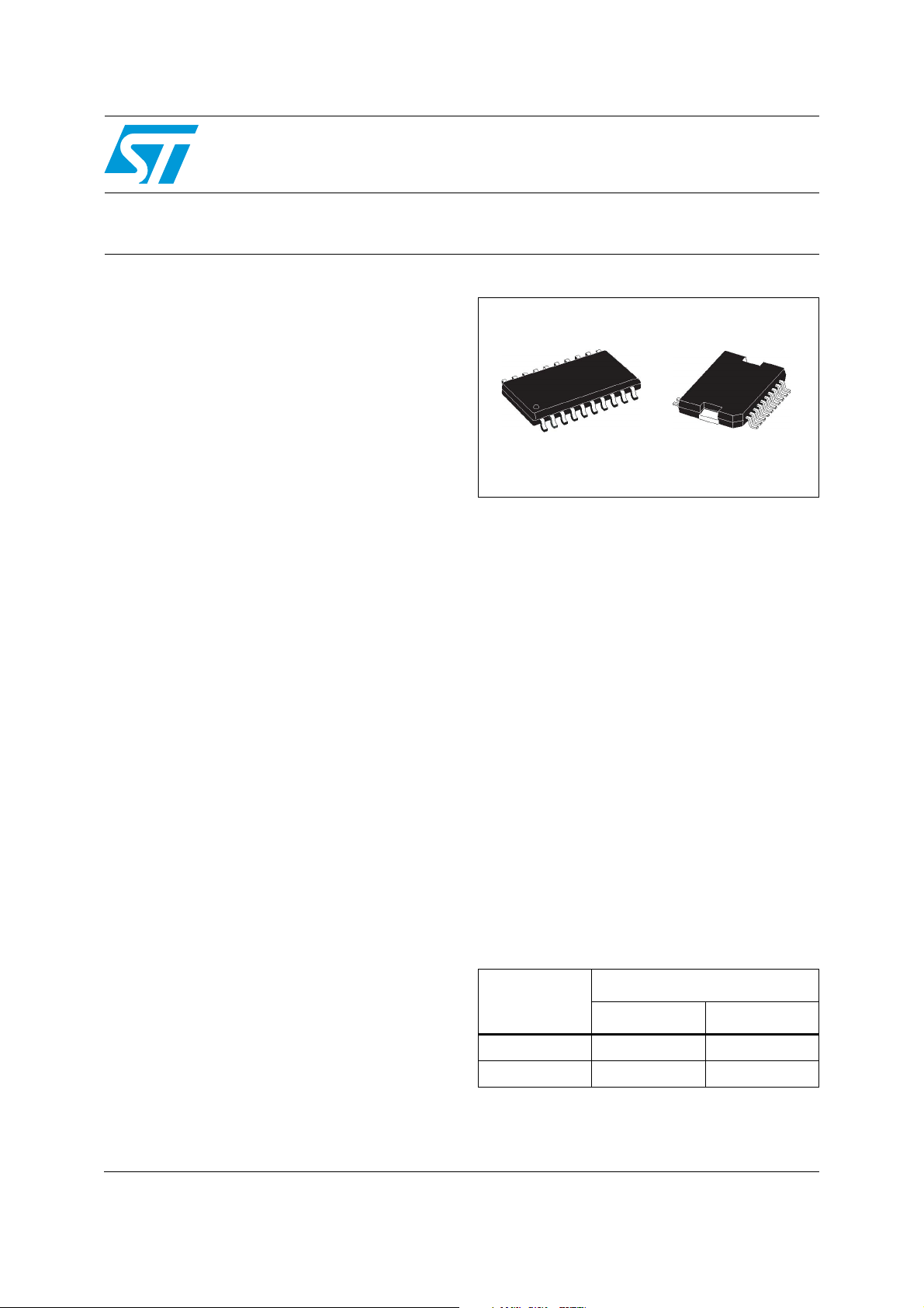
L4938ED
L4938EPD
Advanced voltage regulator
SO-20
Description
The L4938ED and L4938EPD are monolithic
integrated dual voltage regulators with two very
low dropout outputs and additional functions such
as power-on reset and input voltage sense. They
are designed for supplying microcomputer
controlled systems especially in automotive
applications.
PowerSO-20
Table 1. Device summary
Order codes
Package
Tube Tape and reel
SO-20 L4938ED L4938ED013TR
PowerSO-20 L4938EPD L4938EPD13TR
March 2010 Doc ID 17243 Rev 1 1/20
www.st.com
1

Contents L4938ED, L4938EPD
Contents
1 Block diagram and pin description . . . . . . . . . . . . . . . . . . . . . . . . . . . . . 5
2 Electrical specifications . . . . . . . . . . . . . . . . . . . . . . . . . . . . . . . . . . . . . . 7
2.1 Absolute maximum ratings . . . . . . . . . . . . . . . . . . . . . . . . . . . . . . . . . . . . . 7
2.2 Thermal data . . . . . . . . . . . . . . . . . . . . . . . . . . . . . . . . . . . . . . . . . . . . . . . 8
2.3 Electrical characteristics . . . . . . . . . . . . . . . . . . . . . . . . . . . . . . . . . . . . . . . 8
3 Application information . . . . . . . . . . . . . . . . . . . . . . . . . . . . . . . . . . . . . 11
3.1 Functional description . . . . . . . . . . . . . . . . . . . . . . . . . . . . . . . . . . . . . . . 11
3.2 Standby regulator . . . . . . . . . . . . . . . . . . . . . . . . . . . . . . . . . . . . . . . . . . 11
3.3 Output 2 voltage . . . . . . . . . . . . . . . . . . . . . . . . . . . . . . . . . . . . . . . . . . . 12
3.4 Reset circuit . . . . . . . . . . . . . . . . . . . . . . . . . . . . . . . . . . . . . . . . . . . . . . . 12
3.5 Sense comparator . . . . . . . . . . . . . . . . . . . . . . . . . . . . . . . . . . . . . . . . . . 13
3.6 Thermal protection . . . . . . . . . . . . . . . . . . . . . . . . . . . . . . . . . . . . . . . . . 13
3.7 Transient sensitivity . . . . . . . . . . . . . . . . . . . . . . . . . . . . . . . . . . . . . . . . . 13
3.8 Input protection . . . . . . . . . . . . . . . . . . . . . . . . . . . . . . . . . . . . . . . . . . . . 15
4 Package and packing information . . . . . . . . . . . . . . . . . . . . . . . . . . . . . 16
4.1 ECOPACK® packages . . . . . . . . . . . . . . . . . . . . . . . . . . . . . . . . . . . . . . . 16
4.2 SO-20 package information . . . . . . . . . . . . . . . . . . . . . . . . . . . . . . . . . . . 16
4.3 PowerSO-20 package information . . . . . . . . . . . . . . . . . . . . . . . . . . . . . . 17
5 Revision history . . . . . . . . . . . . . . . . . . . . . . . . . . . . . . . . . . . . . . . . . . . 19
2/20 Doc ID 17243 Rev 1

L4938ED, L4938EPD List of tables
List of tables
Table 1. Device summary . . . . . . . . . . . . . . . . . . . . . . . . . . . . . . . . . . . . . . . . . . . . . . . . . . . . . . . . . . 1
Table 2. Pin definitions and functions . . . . . . . . . . . . . . . . . . . . . . . . . . . . . . . . . . . . . . . . . . . . . . . . . 6
Table 3. Absolute maximum ratings . . . . . . . . . . . . . . . . . . . . . . . . . . . . . . . . . . . . . . . . . . . . . . . . . . 7
Table 4. Thermal data. . . . . . . . . . . . . . . . . . . . . . . . . . . . . . . . . . . . . . . . . . . . . . . . . . . . . . . . . . . . . 8
Table 5. OUT1 . . . . . . . . . . . . . . . . . . . . . . . . . . . . . . . . . . . . . . . . . . . . . . . . . . . . . . . . . . . . . . . . . . 8
Table 6. OUT2 . . . . . . . . . . . . . . . . . . . . . . . . . . . . . . . . . . . . . . . . . . . . . . . . . . . . . . . . . . . . . . . . . . 8
Table 7. OUT1, OUT2. . . . . . . . . . . . . . . . . . . . . . . . . . . . . . . . . . . . . . . . . . . . . . . . . . . . . . . . . . . . . 9
Table 8. Enable input . . . . . . . . . . . . . . . . . . . . . . . . . . . . . . . . . . . . . . . . . . . . . . . . . . . . . . . . . . . . . 9
Table 9. Reset circuit . . . . . . . . . . . . . . . . . . . . . . . . . . . . . . . . . . . . . . . . . . . . . . . . . . . . . . . . . . . . . 9
Table 10. Sense comparator . . . . . . . . . . . . . . . . . . . . . . . . . . . . . . . . . . . . . . . . . . . . . . . . . . . . . . . 10
Table 11. SO-20 mechanical data . . . . . . . . . . . . . . . . . . . . . . . . . . . . . . . . . . . . . . . . . . . . . . . . . . . 16
Table 12. PowerSO-20 mechanical data . . . . . . . . . . . . . . . . . . . . . . . . . . . . . . . . . . . . . . . . . . . . . . 17
Table 13. Document revision history . . . . . . . . . . . . . . . . . . . . . . . . . . . . . . . . . . . . . . . . . . . . . . . . . 19
Doc ID 17243 Rev 1 3/20

List of figures L4938ED, L4938EPD
List of figures
Figure 1. Block diagram . . . . . . . . . . . . . . . . . . . . . . . . . . . . . . . . . . . . . . . . . . . . . . . . . . . . . . . . . . . . 5
Figure 2. Configuration diagram (top view) . . . . . . . . . . . . . . . . . . . . . . . . . . . . . . . . . . . . . . . . . . . . . 5
Figure 3. Application diagram . . . . . . . . . . . . . . . . . . . . . . . . . . . . . . . . . . . . . . . . . . . . . . . . . . . . . . 11
Figure 4. OUT2 . . . . . . . . . . . . . . . . . . . . . . . . . . . . . . . . . . . . . . . . . . . . . . . . . . . . . . . . . . . . . . . . . 12
Figure 5. Reset generator . . . . . . . . . . . . . . . . . . . . . . . . . . . . . . . . . . . . . . . . . . . . . . . . . . . . . . . . . 14
Figure 6. Waveforms . . . . . . . . . . . . . . . . . . . . . . . . . . . . . . . . . . . . . . . . . . . . . . . . . . . . . . . . . . . . . 14
Figure 7. Input protection . . . . . . . . . . . . . . . . . . . . . . . . . . . . . . . . . . . . . . . . . . . . . . . . . . . . . . . . . . 15
Figure 8. Input characteristics of SI, EN . . . . . . . . . . . . . . . . . . . . . . . . . . . . . . . . . . . . . . . . . . . . . . 15
Figure 9. SO-20 package dimensions . . . . . . . . . . . . . . . . . . . . . . . . . . . . . . . . . . . . . . . . . . . . . . . . 17
Figure 10. PowerSO-20 package dimensions . . . . . . . . . . . . . . . . . . . . . . . . . . . . . . . . . . . . . . . . . . . 18
4/20 Doc ID 17243 Rev 1
L4938ED, L4938EPD Block diagram and pin description
1 Block diagram and pin description
Figure 1. Block diagram
Figure 2. Configuration diagram (top view)
CT
EN
GND
GND
GND
GND
RES
SO
1
2
3
4
5
6
7
8
9
10
20
19
18
17
16
15
14
13
12
11
SIPR
V
S1
V
S2
GND
GND
GND
GND
N.C.
OUT2
ADJOUT1
N.C.
GND
SO-20
1
2
V
S2
V
S1
SI
PR
CT
EN
3
4
5
6
7
8
9
10
20
19
18
17
16
15
14
13
12
11
GNDGND
N.C.N.C.
OUT2
ADJ
OUT1
SO
RESET
N.C.
N.C.
GND
PowerSO-20
Doc ID 17243 Rev 1 5/20
Block diagram and pin description L4938ED, L4938EPD
Table 2. Pin definitions and functions
PIn number
Name Function
SO-20 PowerSO-20
18 3 V
19 4 V
Supply voltage (400 mA regulator)
S2
Supply voltage (100 mA regulator, reset, sense)
S1
20 5 SI Sense input
1 6 PR Reset threshold programming
2 7 CT Reset delay capacitor
3 8 EN Enable (low activates the 400 mA regulator)
4, 5, 6, 7, 14, 15,
16, 17
1, 10, 11, 20 GND Ground
8 14 RES Reset output
9 15 SO Sense output
10 16 OUT1 100 mA regulator output
11 17 ADJ Feedback of 400 mA regulator
12 18 OUT2 400 mA regulator output
13 2, 9, 19 NC Not connected
6/20 Doc ID 17243 Rev 1

L4938ED, L4938EPD Electrical specifications
2 Electrical specifications
2.1 Absolute maximum ratings
Stressing the device above the ratings listed in the “Absolute maximum ratings” tables may
cause permanent damage to the device. These are stress ratings only and operation of the
device at these or any other conditions above those indicated in the Operating sections of
this specification is not implied. Exposure to the conditions in this section for extended
periods may affect device reliability. Refer also to the STMicroelectronics SURE Program
and other relevant quality documents.
Table 3. Absolute maximum ratings
Symbol Parameter Value Unit
V
INDC
V
INTR
I
O
V
SI
I
SI
V
EN
I
EN
, VSO Output voltages -0.3 to 20 V
V
RES
, ISO Output currents (output low) 5 mA
I
RES
P
O
T
stg
T
J
T
JSD
DC operating supply voltage 28 V
Transient operating supply voltage (T < 400 ms) -14 to 40 V
Output current internally limited
(2)
(1)
(1)
(1)
(1)
Sense input voltage (voltage forced)
Sense input current (current forced)
Enable input voltage (voltage forced)
Sense input current (current forced)
Power dissipation at T
amb
=80°C
Storage temperature -65 to 150 °C
Operating junction temperature -40 to 150 °C
Thermal shutdown junction temperature output 2 will
shutdown typically at TJ 10 K lower than output 1
1. Current forced means voltage unlimited but current limited to the specified value voltage forced
means voltage limited to the specified values while the current is not limited
2. Typical value soldered on a PC board with 8 cm2 copper ground plane (35 mm thick).
Note: The circuit is ESD protected according to MIL-STD-883C.
-20 to 20 V
±1 mA
-20 to 20 V
±1 mA
875 mW
165 °C
Doc ID 17243 Rev 1 7/20

Electrical specifications L4938ED, L4938EPD
2.2 Thermal data
Table 4. Thermal data
Symbol Parameter SO-20 PowerSO-20 Unit
R
thj-amb
R
thj-case
Thermal resistance junction to ambient 50 - °C/W
Thermal resistance junction to case - < 2 °C/W
Note: Typical value soldered on a PC board with 8 cm2 copper ground plane (35 mm thick).
2.3 Electrical characteristics
VS = 14 V; Tj = -40 to 150 °C, unless otherwise specified.
Table 5. OU T1
Symbol Parameter Test condition Min. Typ. Max. Unit
V
= 6 to 28 V;
V
V
V
V
I
DP1
OL01
LIM1
QSB
Supply output voltage
O1
Drop output voltage 1
Load regulation 1
Current limit 1 V
Quiescent current in
standby mode
S
IO1 = 400 µA to 100 mA
T
≤ 125°C;
J
IO1 = 50 to 400 µA
I
= 10 mA 0.1 0.2 V
OUT1
I
= 100 mA; VS = 4.8 V 0.2 0.4 V
OUT1
= 1 to 100 mA (after
I
OUT1
regulation setting)
= 0.8 to 4.5 V 100 200 400 mA
OUT1
I
≥ 2.4 V (output 2 disabled)
EN
IO1 = 0.1 mA; V
T
<85°C; RPR = 0 75 µA
J
> 1.3 V
SI
4.9 5 5.1 V
4.8 5 5.2 V
25 mV
65 90 µA
Table 6. OU T2
Symbol Parameter Test condition Min. Typ. Max. Unit
V
V
V
OL02
R
I
LIM2
O2
DP2
ADJ
I
Q
Output voltage 2 ADJ
connected to OUT2
Drop output voltage 2
Load regulation 2
Adjust input resistance 60 100 150 mA
Current limit 2 V02 = 0.8 to 4.5 V 450 650 1300 mA
Quiescent current
Enable = low; V
IO2 = 5 to 400 mA
I
= 100 mA 0.2 0.3 V
OUT2
I
= 400 mA; VS = 4.8 V 0.3 0.6 V
OUT2
= 5 to 400 mA
I
OUT1
(after regulation setting)
= 100 mA;
I
OUT1
= 400 mA
I
OUT2
8/20 Doc ID 17243 Rev 1
= 6 to 28 V;
S
4.9 5.1 V
50 mV
20 mA

L4938ED, L4938EPD Electrical specifications
Table 7. OUT1, OUT2
Symbol Parameter Test condition Min. Typ. Max. Unit
= 6 to 28 V; IO1 = 1 mA,
V
S
V
OLi 1,2
Table 8. Enable input
Line regulation
Symbol Parameter Test condition Min. Typ. Max. Unit
IO2 = 5 mA,
(after regulation setting)
20 mV
V
ENL
V
ENH
V
ENhyst
I
EN LOW
I
EN HIGH
Table 9. Reset circuit
Enable input low voltage
(output 2 active)
-20 1 V
Enable input high voltage 1.4 20 V
Enable hysteresis 20 30 60 mV
Enable input current low V
Enable input current high
= 0 -20 -8 -3 µA
EN
= 1.1 to 7 V;
V
EN
< 130 °C;
T
J
= 1.1 to 7 V;
V
EN
= 130 to 150 °C;
T
J
-1 0 1 µA
-10 0 10 µA
Symbol Parameter Test condition Min. Typ. Max. Unit
V
-
VO1-
RPR = ∞ 4.5
Reset threshold voltage
V
RT
V
Reset threshold hysteresis RPR = ∞ 30 60 120 mV
RTH
t
RD min
t
RD nom
t
RR
ICT
Reset pulse delay C
Reset pulse delay C
Reset reaction time C
Pull down capability of the
discharge circuit
(1)
= 0 3.65 3.8 3.95 V
R
PR
= 47 nF; t r ≤ 30 µs
RES
= 47 nF
RES
= 47 nF 10 50 150 µs
RES
V
OUT1
(3)
< VRT 3 6 15 mA
(2)
40 60 100 ms
60 100 140 ms
O1
0.3
0.2
V
I
CT
V
RESL
V
RESH
1. The reset threshold can be programmed continuously from typ 3.8 V to 4.7 V by changing a value of an
external resistor from pin PR to GND.
2. This is a minimum reset time according to the hysteresis of the comparator. Delay time starts with V
exceeding VRT.
3. This is the nominal reset time depending on the discharging limit of CT (saturation voltage) and the upper
threshold of the timer comparator. Delay time starts with V
Charge current V
Reset output low voltage
Reset output high leakage
current
> VRT -1.3 -1 0.7 µA
OUT1
= 10 KΩ to V
R
RES
V
≥ 1.5 V
OUT1
V
= 5 V 1 µA
RES
OUT1
exceeding VRT.
OUT1
0.4 V
OUT1
Doc ID 17243 Rev 1 9/20

Electrical specifications L4938ED, L4938EPD
Table 10. Sense comparator
Symbol Parameter Test condition Min. Typ. Max. Unit
V
Functional range -20 20 V
SI
Falling edge; T
V
Sense threshold voltage
SIT
Sense threshold hysteresis 10 30 60 mV
V
SITH
V
Sense output low voltage
SOL
Sense output leakage VSO = 5 V; VSI ≥ 1.5 V 1 µA
I
SOH
Falling edge;
< 130 to 150 °C
T
J
≤ 1.05 V; RSO =10KΩ
V
SI
connected to 5 V; V
VSI = 1.1 to 7 V; TJ < 130 °C -1 0 1 µA
Sense input current high
I
SI HIGH
V
= 1.1 to 7 V;
SI
TJ < 130 to 150 °C
I
SI LOW
Sense input current low VSI = 0 V -20 -8 -3 µA
< 130 °C 1.08 1.16 1.24 V
J
1.05 1.16 1.29 V
≥ 5V
S
0.4 V
-10 0 10 µA
10/20 Doc ID 17243 Rev 1

L4938ED, L4938EPD Application information
3 Application information
Figure 3. Application diagram
(See note 2)
(See note 1)
1. The leakage of CT must be less than 0.5 mA (2 V). If an external resistor between CT and V
the leakage current may be increased. The external resistor should have more than 30 KΩ.
For stability: Cs ≥ 1µF, C01 ≥ 10 µF, C02 ≥ 10 µF, ESR ≤ 5Ω (designed target).
2. For transients exceeding 20 V or -20 V external protection is required at the pins SI and EN as shown at
pin EN. The protection proposed provides proper function for transients in the range of ±200 V. If the zener
diode is omitted the external resistor should be raised to 200 KΩ to limit the current to 1 mA. Without the
zener diode, the function 20 V or -20 V can not be guaranteed.
3.1 Functional description
The L4938ED and L4938EPD are monolithic integrated dual voltage regulators, based on
the STM modulator voltage regulator approach. Several outstanding features and auxiliary
functions are implemented to meet the requirements of supplying microprocessor systems
in automotive applications. Nevertheless, it is suitable also in other applications where two
stabilized voltages are required. The modular approach of this device allows to get easy
also other features and functions when required.
3.2 Standby regulator
The standby regulator uses an isolated collector vertical PNP transistor as a regulating
element. With this structure very low dropout voltage at currents up to 100 mA is obtained.
The dropout operation of the standby regulator is maintained down to 3 V input supply
voltage. The output voltage is regulated up to the transient input supply voltage of 40 V. With
this feature no functional interruption due to overvoltage pulses is generated.
OUT1
is applied,
Doc ID 17243 Rev 1 11/20

Application information L4938ED, L4938EPD
In the standby mode when the output 2 is disabled, the current consumption of the device
(quiescent current) is less than 90 µA (14 V supply voltage).
To reduce the quiescent current peak in the undervoltage region and to improve the
transient response in this region, the dropout voltage is controlled. A second regulation path
keeps the output voltage without load below 5.5 V even at high temperatures.
3.3 Output 2 voltage
The output 2 regulator uses the same output structure as the standby regulator but rated for
the output current of 400 mA. The output voltage is internally fixed to 5 V if ADJ is
connected to V
Figure 4. OUT2
. The output 2 regulator can be switches OFF via the enable input.
OUT2
Connecting a resistor divider R
, R2E to the ADJ, OUT2 pin the output voltage 2 can be
1E
programmed to the value of
⎛⎞
1
⎜⎟
OUT1
⎝⎠
= 4.95 to 5.05 V. For an exact calculation the
with R
= 60 K to 150 K and V
ADJ
temperature coefficient (T
V
OUT2
- 2000 pprm) of the internal resistor (R
C
V
=
OUT1
account. Pin ADJ in this mode should not have a capacitive burden because this would
reduce the phase margin of the regulator loop.
3.4 Reset circuit
The reset circuit supervises the standby output voltage. The reset output (RES) is defined
from V
V
OUT1
The reset threshold of 4.7 V is defined with the internal reference voltage
output divider, when pin PR is left open. The reset threshold voltage can be programmed in
the range from 3.8 V to 4.7 V by connecting an external resistor from pin PR to GND.
12/20 Doc ID 17243 Rev 1
≥ 1 V. Even if V
OUT
.
is lacking, the reset generator is supplied by the output voltage
S
R
1ER2ERADJ
------------------------------------------------ -+
+()
⋅
R
2ERADJ
) must be taken into
ADJ
(a)
and standby

L4938ED, L4938EPD Application information
The value of the programming resistor RPR can be calculated with:
R
PR
3.8V V
22K
--------------------- - 92.9K–=
4.7K
------------ 1–
V
RT
RT
4.7V≤≤
The reset pulse delay time tRD, is defined with the charge time of an external capacitor CT:
CT0.6V⋅
t
RDmin
------------------------=
1μ A
CT1.4V⋅
t
RDnom
------------------------=
1μ A
The reaction time of the reset circuit originates from the noise immunity. Standby output
voltage drops below the reset threshold only a bit longer than the reaction time results in a
shorter reset delay time. The nominal reset delay time is generated for standby output
voltage drops longer than approximately 50 µs. The minimum reset time is generated if reset
condition only occurs for a short time triggering a reset pulse but not completely discharging
C
. The reset can be related to output2 on request. If higher charge currents for the reset
T
capacitor are required a resistors from pin C
to OUT1, may be used to increase the current.
T
We recommended the use of 10 KΩ to 5 V as an output pull up.
3.5 Sense comparator
The sense comparator compares an input signal with an internal voltage reference of typical
1.23 V. The use of an external voltage divider makes this comparator very flexible in the
application. It can be used to supervise the input voltage either before or after the protection
diode and to give additional information to the microprocessor like low voltage warnings. We
recommended the use of 10 KΩ to 5 V as an output pull up.
3.6 Thermal protection
Both outputs are provided with an overtemperature shutdown regulation power dissipation
down to uncritical values. Output 2 shuts down approximately 10 K before output 1. Under
normal conditions shutdown of output 2 allows the chip to cool down again. Thus output 1 is
unaffected. The thermal shutdown reduces the output voltages until power dissipation and
the flow of thermal energy out of the chip balance.
3.7 Transient sensitivity
In proper operation (V
sensitivity to input transients.
> 4.5 V) the reference is supplied by V
OUT
thus reducing
OUT1
a. The reference is alternatively supplied from VS or V
Doc ID 17243 Rev 1 13/20
. If one supply is present, the reference is operating.
OUT1

Application information L4938ED, L4938EPD
Figure 5. Reset generator
Figure 6. Waveforms
14/20 Doc ID 17243 Rev 1

L4938ED, L4938EPD Application information
3.8
Input protection
The Inputs Enable (EN) and Sense In (SI) are protected against negative transients.
Figure 7 is showing the simplified schematic
Figure 7. Input protection
Figure 8. Input characteristics of SI, EN
Doc ID 17243 Rev 1 15/20

Package and packing information L4938ED, L4938EPD
4 Package and packing information
4.1 ECOPACK® packages
In order to meet environmental requirements, ST offers these devices in different grades of
ECOPACK
®
packages, depending on their level of environmental compliance. ECOPACK®
specifications, grade definitions and product status are available at: www.st.com
ECOPACK
®
is an ST trademark.
4.2 SO-20 package information
Table 11. SO-20 mechanical data
Dim.
Min. Typ. Max.
A 2.35 2.65
A1 0.1 0.3
B 0.33 0.51
C 0.23 0.32
D 12.6 13
E 7.4 7.6
.
mm
e 1.27
H 10 10.65
h 0.25 0.75
L 0.4 1.27
K 0° 8°
16/20 Doc ID 17243 Rev 1

L4938ED, L4938EPD Package and packing information
Figure 9. SO-20 package dimensions
4.3 PowerSO-20 package information
Table 12. PowerSO-20 mechanical data
Dim.
Min. Typ. Max.
A 3.6
a1 0.1 0.3
a2 3.3
a3 0 0.1
b 0.4 0.53
c 0.23 0.32
(1)
D
15.8 16
D1 9.4 9.8
E 13.9 14.5
e 1.27
e3 11.43
E1 (1) 10.9 11.1
E2 2.9
E3 5.8 6.2
mm
Doc ID 17243 Rev 1 17/20

Package and packing information L4938ED, L4938EPD
Table 12. PowerSO-20 mechanical data (continued)
mm
Dim.
Min. Typ. Max.
G 0 0.1
H 15.5 15.9
h 1.1
L 0.8 1.1
N 10°
S 8°
T 10
1. "D and F" do not include mold flash or protrusions.
- Mold flash or protrusions shall not exceed 0.15 mm (0.006").
- Critical dimensions: "E", "G" and "a3"
Figure 10. PowerSO-20 package dimensions
DETAIL B
R
c
a1
E
lead
DETAIL A
NN
a2
A
b
DETAIL A
e3
H
e
E2
h x 45˚
D
1120
E1
T
110
PSO20MEC
a3
Gage Plane
BOTTOM VIEW
DETAIL B
0.35
S
D1
slug
- C -
L
SEATING PLANE
GC
(COPLANARITY)
E3
0056635 I
18/20 Doc ID 17243 Rev 1

L4938ED, L4938EPD Revision history
5 Revision history
Table 13. Document revision history
Date Revision Changes
10-Mar-2010 1 Initial release.
Doc ID 17243 Rev 1 19/20

L4938ED, L4938EPD
Please Read Carefully:
Information in this document is provided solely in connection with ST products. STMicroelectronics NV and its subsidiaries (“ST”) reserve the
right to make changes, corrections, modifications or improvements, to this document, and the products and services described herein at any
time, without notice.
All ST products are sold pursuant to ST’s terms and conditions of sale.
Purchasers are solely responsible for the choice, selection and use of the ST products and services described herein, and ST assumes no
liability whatsoever relating to the choice, selection or use of the ST products and services described herein.
No license, express or implied, by estoppel or otherwise, to any intellectual property rights is granted under this document. If any part of this
document refers to any third party products or services it shall not be deemed a license grant by ST for the use of such third party products
or services, or any intellectual property contained therein or considered as a warranty covering the use in any manner whatsoever of such
third party products or services or any intellectual property contained therein.
UNLESS OTHERWISE SET FORTH IN ST’S TERMS AND CONDITIONS OF SALE ST DISCLAIMS ANY EXPRESS OR IMPLIED
WARRANTY WITH RESPECT TO THE USE AND/OR SALE OF ST PRODUCTS INCLUDING WITHOUT LIMITATION IMPLIED
WARRANTIES OF MERCHANTABILITY, FITNESS FOR A PARTICULAR PURPOSE (AND THEIR EQUIVALENTS UNDER THE LAWS
OF ANY JURISDICTION), OR INFRINGEMENT OF ANY PATENT, COPYRIGHT OR OTHER INTELLECTUAL PROPERTY RIGHT.
UNLESS EXPRESSLY APPROVED IN WRITING BY AN AUTHORIZED ST REPRESENTATIVE, ST PRODUCTS ARE NOT
RECOMMENDED, AUTHORIZED OR WARRANTED FOR USE IN MILITARY, AIR CRAFT, SPACE, LIFE SAVING, OR LIFE SUSTAINING
APPLICATIONS, NOR IN PRODUCTS OR SYSTEMS WHERE FAILURE OR MALFUNCTION MAY RESULT IN PERSONAL INJURY,
DEATH, OR SEVERE PROPERTY OR ENVIRONMENTAL DAMAGE. ST PRODUCTS WHICH ARE NOT SPECIFIED AS "AUTOMOTIVE
GRADE" MAY ONLY BE USED IN AUTOMOTIVE APPLICATIONS AT USER’S OWN RISK.
Resale of ST products with provisions different from the statements and/or technical features set forth in this document shall immediately void
any warranty granted by ST for the ST product or service described herein and shall not create or extend in any manner whatsoever, any
liability of ST.
ST and the ST logo are trademarks or registered trademarks of ST in various countries.
Information in this document supersedes and replaces all information previously supplied.
The ST logo is a registered trademark of STMicroelectronics. All other names are the property of their respective owners.
© 2010 STMicroelectronics - All rights reserved
STMicroelectronics group of companies
Australia - Belgium - Brazil - Canada - China - Czech Republic - Finland - France - Germany - Hong Kong - India - Israel - Italy - Japan -
Malaysia - Malta - Morocco - Philippines - Singapore - Spain - Sweden - Switzerland - United Kingdom - United States of America
www.st.com
20/20 Doc ID 17243 Rev 1
 Loading...