

5V–1A VERY LOW DROPREGULATOR
.
VERY LOW DROP (max. 0.9V at 1A) OVER
FULL OPERATING TEMPERATURE RANGE
(– 40/ + 125 °C)
.LOW QUIESCENT CURRENT (max 70 mA at
1 A) OVERFULLTRANGE
.
PRECISEOUTPUTVOLTAGE(5V±4%)OVER
FULLT RANGE
.
POWER ON-OFF INFORMATION WITH SETTABLEDELAY
.
INHIBIT FOR REMOTE ON-OFF COMMAND
(activehigh)
.LOADSTANDBYCURRENT
.LOAD DUMPAND REVERSEBATTERYPRO-
TECTION
.
SHORTCIRCUITPROTECTION
.THERMAL SHUTDOWN
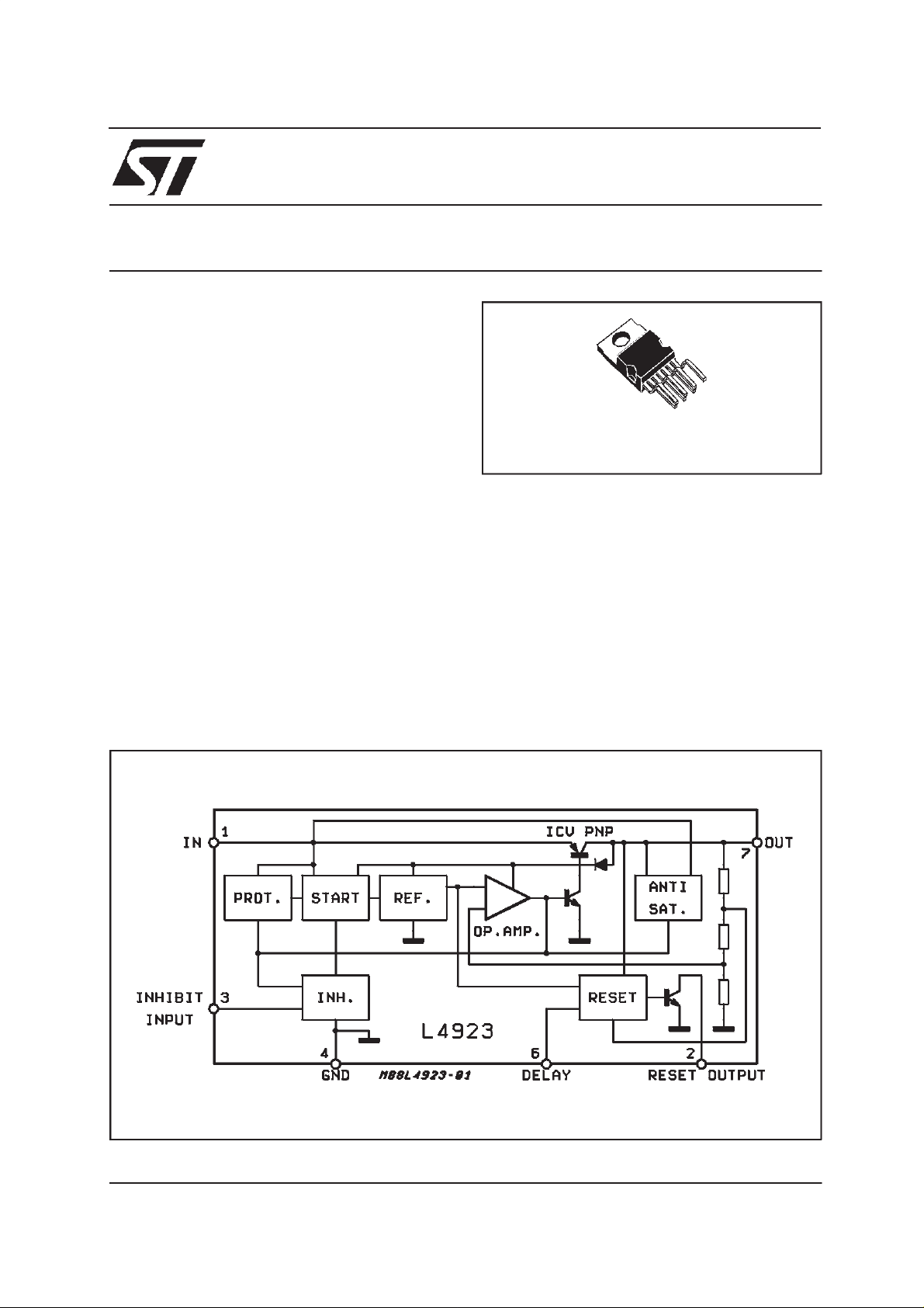
DESCRIPTION
TheL4923isa highcurrentmonolithicvoltageregulatorwith verylow voltagedrop(0.70 V max at 1 A,
=25°C).
T
J
L4923
WITHRESET AND INHIBIT
Hept aw att
ORDERING NUMBER : L492 3
The device is internally protected against load
dumps transient of + 60 V, input overvoltage, reversepolarity,overheatingandoutputshortcircuit:
thankstothesefeaturesthe L4923is verysuitedfor
theautomotiveand industrialapplications.
The reset function is very useful for power off and
poweron informationwhen supplyinga microprocessor.
The inhibit function reduces drastically the consumptionwhenno loadcurrentisrequired: typically
thestandbycurrentvalueis 300µA.
BLOCK DIAGRAM
June 2000
Thisis advanced informationon a new product now in development or undergoing evaluation. Detailsaresubjectto change withoutnotice.
1/6
L4923
ABSOLUTE MAXIMUM RATINGS
Symbol Parameter Value Unit
V
V
V
D
T
J
T
op
T
stg
Note:The circuit isESD protectedaccording to MIL-STD-883C
THERMAL DATA
Symbol Parameter Value Unit
R
th j-case
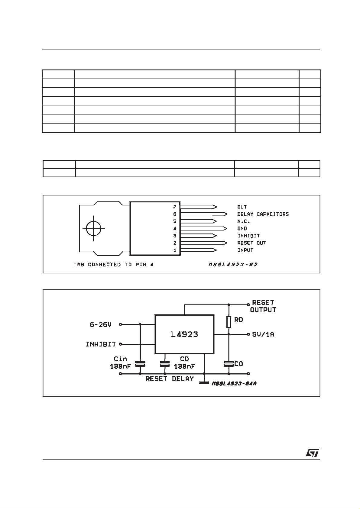
PI N CONNECTION
DC Input Voltage 35 V
i
DC Reverse Voltage – 18 V
r
Positive Load Dump Protection (t = 300ms) 60 V
Junction Temperature range – 40 to 150
Operating Temperature Range – 40 to 125
Storage Temperature Range – 55 to 150
Thermal Resistance Junction Case 4
C/W
°
°C
°C
°C
Figure1 : ApplicationCircuit.
(*)RECOMMENDED VALUE : C0=47µF, ESR <10Ω,(I
2/6
> 10 mA) OVER FULL T
out
range
.

L4923
ELECTRICAL CHARACTERISTICS (Vi= 14. 4V, – 40°C ≤ TJ≤ + 125°C unless otherwise specified)
Symbol Parameter Test Conditions Min. Typ. Max. Unit
V
V
o
V
∆
Line
SVR Supply Voltage Rejection I
V
∆
LOAD
V
i–Vo
I
q
I
SC
SVR Supply Volt. Rej. I
V
R
V
RT peak
I
R
t
D
V
RthOFF
I
C6
V
RthON
V
6
V
6H
V
InhL
V
InhH
I
InhL
Operating Input Voltage (*) Note 1 6 26 V
i
Output Voltage Io= 0mA to 1A
=25°C
T
J
4.8
4.9
Line Regulation Vi= 6 to 26V; IO= 10mA 5 25 mV
= 700mA
o
f = 120Hz; C
= 12Vdc+5V
V
i
=47µF
o
pp
55 dB
Load Regulation Io= 10mA to 1A 15 50 mV
Dropout Voltage
=25°C, IO=1A
T
J
Over Full T, I
Quiescent Current Io= 10mA
=1A
I
o
Active High Inhibit
= 1A 0.90 V
o
0.45 0.70 V
7
25
0.30
Short Circuit Current 1.8 A
= 350mA ; f = 120Hz
o
= 100µF;Vi= 12V±5V
C
o
Rset Output Saturation Voltage 1.5V < VO<V
3V < V
O<VRT (off),IR
Power On-Off Reset out Peak
1KΩ Reset Pull-up to V
RT (off),IR
pp
= 1.6mA
=8mA
O
50 60 dB
0.65 1.0 V
Voltage
Reset Output Leakage Current
(high level)
Voin Regul.
=5V
V
R
Reset Pulse Delay Time CD= 100nF 20 ms
Power OFF VoThreshold Vo@ Reset out H to L
–0.15 V
V
o
Delay Capacitor Charging
Transition; T
–40°C≤T
J
=25°C
J
≤+ 125°C
4.75
4.7
V6=3V 20
Current (current generator)
Power ON VoThreshold Vo@ Reset out L to H
Transition
V
rthOFF
+ 0.03V
Delay Comparator Threshold Reset out = ”1” H toL Transition 3.2 3.8 V
Reset out = ”0” L to H Transition 3.7 4 4.4 V
Delay Comparator Hysteresis 500 mV
Low Inhibit Voltage 0.5 V
High Inhibit Voltage 2.0 V
Low Level Inhibit Current V
= 0.4V – 40 – 10 µ
Inh L
5.2
5.1
12
70
0.65
0.40
0.40
50 µ
V
–
o
0.04V
V
V
mA
mA
mA
V
V
A
V
µA
V
A
(*) Note 1 : The device is notoperating within the range : 26 V < Vi<37V.
EXTERNALCOMPENSATION
Sincethepurposeofa voltageregulatoris tosupply
a fixed output voltage in spite of supply and load
variations,the open loop gainof theregulatormust
beveryhigh atlowfrequencies.This maycauseinstability as a result of the various poles present in
the loop. To avoid this instability dominant pole
compensationisusedtoreducephaseshiftsdueto
other poles at the unity gain frequency. The lower
thefrequencyof theseotherpoles,thegreatermust
be the capacitor used tocreate thedominant pole
for the same DC gain.
Where the output transistor is a lateral PNP type
thereis apole in theregulationloop at a frequency
too low to be compensatedby acapacitorwichcan
be integrated.An external compensationis thereforenecessaryso a veryhigh value capacitormust
be connectedfrom theoutputtoground.
Theparassiticequivalentseriesresistanceofthecapacitorusedaddsa zerotothe regulationloop.This
zero may compromise the stability of the system
sinceits effecttendsto canceltheeffectof thepole
added.InregulatorsthisESRmustbe lessthan3Ω
and the minimumcapacitorvalue is 47µF.
3/6

L4923
FUNCTI O NAL DE SCRI PTION
The operating principle of the voltage regulator is
basedonthereference,theerroramplifier,thedriver
and the power PNP. This stage uses an Isolated
CollectorVerticalPNPtransistorwhichallowsto obtainverylow dropoutvoltage(typ.450 mV) andlow
quiescentcurrent(I
= 20mA typicallyat IO= 1 A).
Q
Thanks to these featuresthe device is particularly
suited when the power dissipation must be limited
as,for example,in automotiveor industrialapplicationssuppliedby battery.
The three gain stages(operationalamplifier, driver
and power PNP) require the external capacitor
(C
=22µF) to guaranteethe globalstabilityof
Omin
the system.
Theantisaturationcircuitallowstoreducedrastically
the currentpeak which takesplace duringthe start
up.
Figure2 : TypicalReset OutputWaveform.
The reset functionis LOW activewhen the output
voltagelevel is lower than the reset threshold voltageV
voltageis higherthanV
(typ.value: VO-150mV).Whentheoutput
Rth
theresetbecomesHIGH
Rth
afteradelaytimesettablewiththeexternalcapacitor
. Typically td= 20 ms, Cd= 0.1 µF. The reset
C
d
threshold hysteresis improves the noise immunity
allowingto avoid falseswitchings.The typicalreset
outputwaveformis shownin fig.2.
TheinhibitcircuitacceptsstandardTTLinputlevels:
thisblockswitchesoffthevoltageregulatorwhenthe
inputsignalis HIGH and switcheson it whenthe inputsignalisLOW.Thankstoinhibitfunctionthecon-
sumptionisdrasticallyreduced(650 µA max)when
no loadcurrentis required.
4/6

L4923
DIM.
MIN. TYP. MAX. MIN. TYP. MAX.
A 4.8 0.189
C 1.37 0.054
D 2.4 2.8 0.094 0.110
D1 1.2 1.35 0.047 0.053
E 0.35 0.55 0.014 0.022
E1 0.7 0.97 0.028 0.038
F 0.6 0.8 0.024 0.031
F1 0.9 0.035
G 2.34 2.54 2.74 0.095 0.100 0.105
G1 4.88 5.08 5.28 0.193 0.200 0.205
G2 7.42 7.62 7.82 0.295 0.300 0.307
H2 10.4
H3 10.05 10.4 0.396 0.409
L 16.7 16.9 17.1 0.657 0.668 0.673
L1 14.92
L2 21.24 21.54 21.84 0.386 0.848 0.860
L3 22.27 22.52 22.77 0.877 0.891 0.896
L4 1.29
L5 2.6 2.8 3 0.102 0.110 0.118
L6 15.1 15.5 15.8 0.594 0.610 0.622
L7 6 6.35 6.6 0.236 0.250 0.260
L9 0.2 0.008
M 2.55 2.8 3.05 0.100 0.110 0.120
M1 4.83 5.08 5.33 0.190 0.200 0.210
V4 40° (typ.)
Dia 3.65 3.85 0.144 0.152
mm inch
0.409
0.587
0.051
OUTLINE AND
MECHANICAL DATA
Heptawatt V
H3
L
VV
E
L1
M1
A
C
D
D1
L2
L5
L3
H1
Dia.
M
F
E1
E
GG1G2
H2
V4
L9
F
L7
L4
L6
F1H2
HEPTAMEC
5/6

L4923
Information furnished is believed to be accurate and reliable. However, STMicroelectronics assumes no responsibility for the consequences of use of such information nor for any infringement of patents or other rights of third parties which may result from its use. No
license is granted by implication or otherwise under any patent or patent rights of STMicroelectronics. Specification mentioned in this
publication are subject to change without notice. This publication supersedes and replaces all information previously supplied. STMicroelectronics products are not authorized for use as critical components in life support devices or systems without express written
approval of STMicroelectronics.
Australia - Brazil - China - Finland - France - Germany - Hong Kong - India - Italy - Japan - Malaysia - Malta - Morocco -
The ST logo is a registered trademark of STMicroelectronics
2000 STMicroelectronics – Printed in Italy – All Rights Reserved
STMicroelectronics GROUP OF COMPANIES
Singapore - Spain - Sweden - Switzerland - United Kingdom - U.S.A.
http://www.st.com
6/6
 Loading...