

Page 1
ADJUSTABLEVOLTAGEREGULATOR PLUS FILTER
.
OUTPUTVOLTAGEADJUSTABLE FROM
4TO11V
.
HIGH OUTPUTCURRENT (up to 250mA)
.
HIGH RIPPLEREJECTION
.
HIGH LOAD REGULATION
.
HIGH LINE REGULATION
.
SHORTCIRCUITPROTECTION
.
THERMAL SHUT DOWN WITH HYSTERESIS
.
DUMP PROTECTION
L4915
PRELIMINARY DATA
DESCRIPTION
This circuit combines both a filter and a voltage
regulatorin order to provide a high ripple rejection
overa wideinput voltage range.
Asupervisorlow-passloopoftheelementprevents
the output transistor from saturation at low input
voltage.
The non linear behaviour of this control circuitry
allowsa fast settling of the filter.
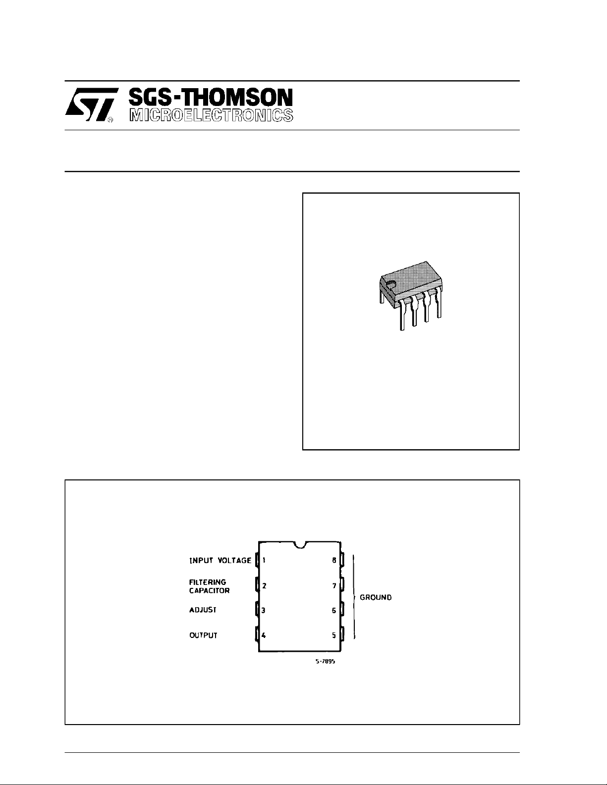
PIN CONNECTION
POWER MINIDIP
ORDERING NUMBER : L4915
June1993
1/7
Page 2
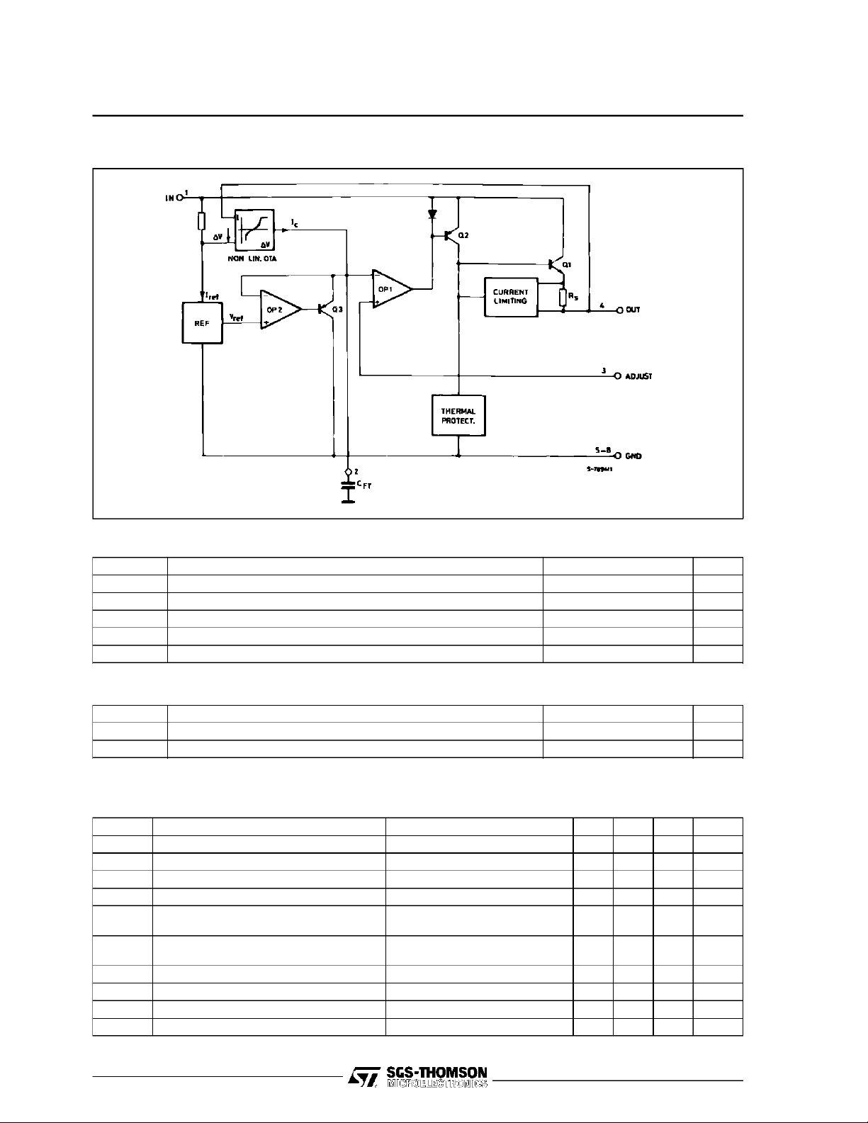
L4915
BLOCKDIAGRAM
ABSOLUTE MAXIMUMRATINGS
Symbol Parameter Value Unit
V
V
I
O
P
tot
T
stg
Peak Input Voltage(300 ms) 40 V
i
DC Input Voltage 28 V
i
Output Current Internally Limited
Power Dissipation Internally Limited
Storage and Junction Temperature – 40 to 150 °C
THERMAL DATA
Symbol Parameter Value Unit
R
th j-amb
R
th j-pins
Thermal Resistance Junction-ambient Max. 80 °C/W
Thermal Resistance Junction-pins Max. 20 °C/W
ELECTRICALCHARACTERISTICS
=25oC; Vi= 13.5 V, VO= 8.5V,circuitof Fig. 1, unless otherwise specified)
(T
amb
Symbol Parameter Test Conditions Min. Typ. Max. Unit
V
Input Voltage 20 V
i
V
∆V
∆V
∆V
∆V
V
∆I
I
Output Voltage Vi= 6 to 18V,Io= 5 to 150mA 4 11 V
o
Controlled Input-output Dropout Voltage Io= 5 to 150mA, Vi= 6 to 10V 1.6 2.1 V
I/O
Line Regulation Vi= 12 to 18V,Io= 10mA 1 20 mV
O
Load Regulation Io= 5 to 250mA,
o
Load Regulation (filter mode) Vi= 8.5V, Io= 5 to 150mA
o
Internal Voltage Reference 2.5 V
ref
I
Quiescent Current Io=5mA 1 2 mA
q
Quiescent CurrentChange Vi= 6 to 18V,Io= 5 to 150mA 0.05 mA
q
Adjust Input Current 40 nA
AD
=30µs, t
t
on
=30µs, t
t
on
= ≥ 1ms
off
=≥ 1ms
off
50 100 mV
150 250 mV
2/7
Page 3

L4915
ELECTRICALCHARACTERISTICS (continued)
=25oC; Vi= 13.5 V, VO= 8.5V,circuitof Fig. 1, unless otherwise specified)
(T
amb
Symbol Parameter Test Conditions Min. Typ. Max. Unit
∆V
O
∆T
SVR Supply Voltage Rejection V
I
T
(*) Depending of the CFTcapacitor
Output VoltageDrift I
Short Circuit Current 250 300 mA
SC
Switch On Time Io= 150mA
on
Thermal ShutdownJunction
T
j
Temperature
= 10mA 1.2 mV/°C
o
=1V
iac
Regulator
Filter Mode
Regulator
Filter Mode
, f = 100Hz, Io= 150mA
RMS
71
35(*)
300
500(*)
145 °C
dB
ms
PRINCIPLE OF OPERATION
Duringnormal operation(inputvoltage upper than
V
I MIN=VOUT NOM
+ ∆V
). The deviceworks as a
I/O
normal voltage regulator built around the OP1 of
the block diagram.
Theseriespasselementuses aPNP-NPNconnection to reduce the dropout. The reference voltage
of the OP1 is derivedfrom a REF throughthe OP2
and Q3, acting as an active zener diode of value
V
.
REF
In this condition the device works in the range (1)
of the characteristicof the non linear drop control
unit (see Figure 1).
Figure1 : NonlinerTransfer Characteristicof
the Drop ControlUnit
Theoutput voltage is fixed to itsnominal value :
V
OUT NOM
= V
REF
1 +
= V
CFT
R1
R2
1+
R1R2
The ripple rejection is quite high (70dB) and independentto C
FT
value.
On the usual voltage regulators, when the input
vol-tagegoes belowthe nominalvalue,theregulation transistors (series element) saturate bringing
the system out of regulation and making it very
sensibleto every variationof the input voltage.On
the contrary,a control loop on theL4915 consents
to avoid the saturation of the series element by
regulating the value of the reference voltage
(pin 2). In fact, whenever the input voltage decreasesbelow (V
the supervisorloop, utilizing
I MIN
a non linear OTA, forces the reference voltage at
pin 2 to decrease by discharging C
. So, during
FT
the staticmode, whentheinputvoltagegoesbelow
thedropout iskept fixedto about1.6 V. Inthis
V
MIN
condition the device works as a low pass filter in
the range (2) of the OTAcharacteristic.The ripple
R1R2
FT
as
rejection is externally adjustable acting on C
follows:
SVR (jΩ) =
V
(jΩ)
i
V
(jΩ)
OUT
= 1 +
jw C
gm
−6
10
1 +
FT
Where:
gm ==2 ⋅ 10
-5Ω-1
OTA’S typical transconductancevalue on
linear region
R1R2= fixed ratio
C
= value of capacitorin µF
FT
The reactiontimeofthe supervisorloop isgivenby
the transconductanceofthe OTAandby C
. When
FT
the value of the ripple voltage is so high and its
negativepeakis fastenoughto determineanistantaneousdecrease of the dropouttill 1.2V,the OTA
works in a higher transconductance condition
[range (3) of the characteristic] anddischargesthe
capacitorrapidously.
If theripplefrequencyis highenoughthecapacitor
won’tcharge itself completely, andthe outputvoltage reaches a smallvalue allowing a betterripple
rejection; thedevice’sagainworkingasafilter (fast
transientrange).
WithC
=10µF; f =100Hz;Vo=8.5V a SVRof 35
FT
is obtained.
3/7
Page 4

L4915
Figure2 : SupplyVoltage Rejection versus
Input Voltage
Figure4 : V
versusSupplyVoltage (VO= 8.5V) Figure 5 : Quiescent Currentversus
O
Figure 3 : SupplyVoltage Rejection versus
Frequency
Input Voltage (V
=8.5V)
O
Figure6 : Dropoutversus Load Current
4/7
Page 5

APPLICATIONCIRCUIT
L4915
5/7
Page 6
L4915
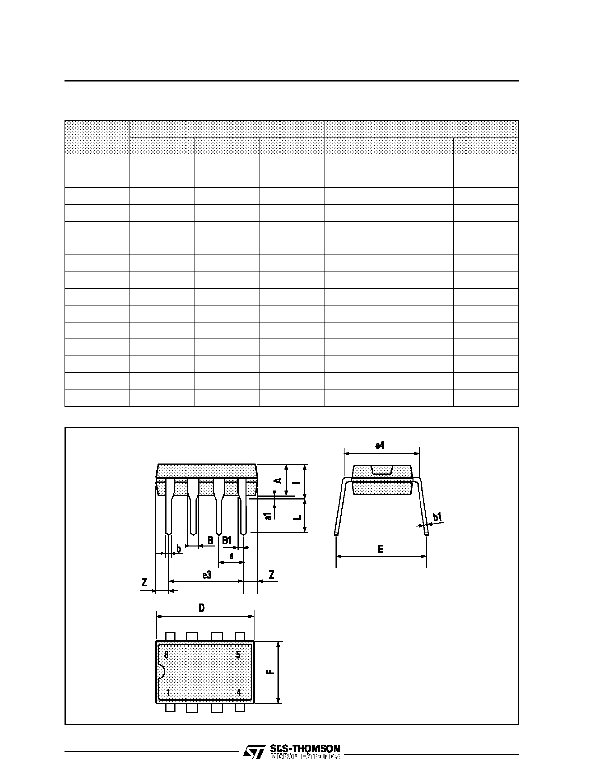
MINIDIP4+4 PACKAGE MECHANICALDATA
DIM.
MIN. TYP. MAX. MIN. TYP. MAX.
A 3.3 0.130
a1 0.7 0.028
B 1.39 1.65 0.055 0.065
B1 0.91 1.04 0.036 0.041
b 0.5 0.020
b1 0.38 0.5 0.015 0.020
D 9.8 0.386
E 8.8 0.346
e 2.54 0.100
e3 7.62 0.300
e4 7.62 0.300
F 7.1 0.280
I 4.8 0.189
L 3.3 0.130
Z 0.44 1.6 0.017 0.063
mm inch
6/7
Page 7

L4915
Information furnished is believed to be accurate and reliable. However, SGS-THOMSON Microelectronics assumes no responsibility for the
consequences of use of such information nor for any infringement of patents or other rights of third parties which may result from its use. No
license is granted by implication or otherwise under any patent or patentrights ofSGS-THOMSON Microelectronics. Specifications mentioned
in this publication are subject to change without notice. This publication supersedes and replaces all information previously supplied.
SGS-THOMSON Microelectronics products are not authorized for useas criticalcomponents inlife support devices or systems without express
written approval of SGS-THOMSON Microelectronics.
1994 SGS-THOMSON Microelectronics - All Rights Reserved
Australia - Brazil - France - Germany - Hong Kong - Italy - Japan - Korea - Malaysia - Malta - Morocco - The Netherlands - Singapore -
SGS-THOMSON Microelectronics GROUP OF COMPANIES
Spain - Sweden- Switzerland - Taiwan - Thaliand -United Kingdom - U.S.A.
7/7
 Loading...