

DUAL5V REGULATOR WITH RESET
.
OUTPUTCURRENTS : I01=400mA
I
=400mA
02
.
FIXEDPRECISIONOUTPUTVOLTAGE
5V±2%
.
RESETFUNCTION CONTROLLED BY INPUT
VOLTAGEAND OUTPUT1 VOLTAGE
.
RESET FUNCTION EXTERNALLY PROGRAMMABLETIMING
.
RESET OUTPUT LEVEL RELATED TO OUTPUT 2
.
OUTPUT 2 INTERNALLY SWITCHED WITH
ACTIVEDISCHARGING
.
LOW LEAKAGE CURRENT, LESS THAN 1µA
ATOUTPUT 1
.
LOWQUIESCENTCURRENT (Input 1)
.
INPUT OVERVOLTAGE PROTECTION UP TO
60V
.
RESETOUTPUT HIGH
.
OUTPUTTRANSISTORSSO A PROTECTION
.
SHORT CIRCUIT AND THERMAL OVERLOADPROTECTION
L4901A
HEPTAWATT (Vertical)
(PlasticPackage)
ORDERING NUMBER : L4901A
DESCRIPTION
The L4901A is a monolithic low drop dual 5V
regulatordesignedmainlyfor supplyingmicroprocessorsystems.
Resetand data savefunctionsduring switchon/off
canbe realized.
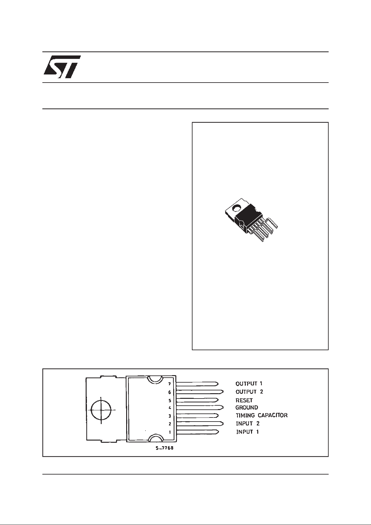
PIN CONNECTION
June 2000
1/10

L4901A
PIN DESCRIPTION
N°
1 Input 1 Low QuiescentCurrent 400mA Regulator Input.
2 Input 2 400mA regulator input.
3 Timing
4 GND Common Ground.
5 Reset
6 Output 2 5V – 400mA Regulator Output. Enabled if V
7 Output 1 5V – 400mA regulatoroutput with Low leakage (in switch-OFF condition).
BLOCKDIAGRAM
Name Function
If Reg. 2 is switched-ON the delay capacitor is charged with a 10µA constant current. When Reg.
Capacitor
2 is switched-OFF the delay capacitor is decharged.
When pin 3 reaches 5V the reset outputis switched high.
Output
Therefore t
the C
RD=Ct
capacitor is discharged.
02
5V
(
); tRD(ms) = Ct(nF)
10µA
1>VRTand V
o
IN 2>VIT
. If Reg. 2 is switched-OFF
SCHEMATIC DIAGRAM
2/10

L4901A
ABSOLUTE MAXIMUMRATINGS
Symbol Parameter Value Unit
V
IN
I
o
T
DC Input Voltage
Transient Input Overvoltage (t = 40ms)
Output Current Internally Limited
Storage and Junction Temperature – 40 to 150
j
THERMAL DATA
Symbol Parameter Value Unit
R
th (j-c)
Thermal Resistance Junction-case Max. 4
24
60
V
V
°C
°C/W
ELECTRICAL CHARACTERISTICS (VIN= 14, 4V, T
=25°C unless otherwise specified)
amb
Symbol Parameter Test Conditions Min. Typ. Max. Unit
DC Operating Input Voltage 20 V
V
i
V
V
V
I
I
L01
I
V
V
V
∆V
∆V
∆V
∆V
I
V
V
V
V
t
∆V
∆
∆V
∆T
SVR1 Supply Voltage Rejection f = 100Hz, V
SVR2 Supply Voltage Rejection 50 80 dB
* The dropoutvoltage is defined as thedifference between theinput and the outputvoltage when theoutput voltage is lowered of 25 mV under
constant output current condition.
Output Voltage 1
01
Output Voltage 2 HIGH
02 H
Output Voltage 2 LOW I02= – 5mA 0.1 V
02 L
Output Current 1
01
Leakage Output 1 Current
Output Current 2 ∆
02
Output 1 Dropout Voltage (*) I01= 10mA
I01
Input Threshold Voltage V01+ 1.2 6.4 V01+ 1.7 V
IT
Input Threshold Voltage Hyst. 250 mV
ITH
Line Regulation 1 7V < VIN< 18V, I01= 5mA 5 50 mV
01
Line Regulation 2 7V < VIN< 18V, I02= 5mA 5 50 mV
02
Load Regulation 1 5mA < I01< 400mA 50 100 mV
01
Load Regulation 2 5mA < I01< 400mA 50 100 mV
02
Quiescent Current
I
Q
Quiescent Current 1
Q1
Reset Threshold Voltage V02– 0.15 4.9 V02–0.05 V
RT
Reset Threshold Hysteresis 30 50 80 mV
RTH
Reset Output Voltage HIGH
RH
Reset Output Voltage LOW IR= –<0>5mA 0.25 0.4 V
RL
Reset Pulse Delay Ct= 10nF 3 5 11 ms
RD
Timing Capacitor Discharge Time Ct= 10nF 20
t
d
01
Thermal Drift
T
02
Thermal Drift
R Load 1kΩ
R Load 1k
= – 100mV
V
∆
01
=0,V01≤ 3V
V
IN
= – 100mV
V
02
= 100mA
I
01
= 300mA
I
01
02=I01
0<V
7V < V
5mA, I
≤
01
= 500µA
R
≤ 5mA
IN
IN
I
I
6.3V < V
I
–20°C≤T
–20°C≤T
Io = 100mA
Ω
< 13V
< 13V
IN
02
< 13V
amb
amb
R
=0,V
≤ 125°C
≤ 125°C
= 0.5V
IN2
=0
4.95 5.05 5.15 V
V01–0.1 5 V
01
400 mA
1
400 mA
0.7
0.8
1.1
4.5
1.6
0.8
1
1.4
6.5
3.5
0.6 0.9 mA
V
– 1 4.12 V
02
02
0.3 –
0.8
0.3 –
0.8
50 84 dB
V
µA
V
V
V
mA
V
µs
mV/°C
mV/°C
3/10

L4901A
TESTCIRCUIT
APPLICATIONINFORMATION
Inpower suppliesfor µPsystems it is necessaryto
provide power continuously to avoid loss of informationin memoriesand in time of dayclocks,or to
savedatawhen theprimarysupplyisremoved.The
L4901A makes it very easy to supply such equipments;it providestwo voltageregulators(both 5 V
high precision) with separate inputs plus a reset
output forthe data savefunction.
CIRCUITOPERATION(see Figure 1)
After switch on Reg. 1 saturatesuntil V
rises to
01
the nominalvalue.
When the input 2 reaches V
higherthanV
the reset output (V
theoutput 2 (V02) switcheson and
RT
) also goes high after a pro-
R
and the output 1 is
IT
Figure1
grammabletime T
V
andVRareswitchedtogetherat lowlevelwhen
02
(timingcapacitor).
RD
one of the followingconditionsoccurs :
- an input overvoltage
- an overloadon the output 1 (V
- a switchoff (V
IN<VIT-VITH
);
01<VRT
);
and they start againas before when the condition
is removed.
An overload on output 2 does not switchReg. 2,
and does not influenceReg.1.
TheV
outputfeatures:
01
- 5 V internal reference without voltage divider
between the output and the error comparator;
- very low drop series regulator element utilizing
current mirrors ;
permit high output impedance and then very low
leakage current error even in power down condi-
4/10

L4901A
tion.
Thisoutputmaythereforebeusedtosupplycircuits
continuously, such as volatile RAMs, allowing the
use of a back-up battery. The V
regulator also
01
featureslowconsumption(0.6 mAtyp.)tominimize
batterydrainin applicationswherethe V
regulator
1
is permanentlyconnectedto a battery supply.
TheV
output can supply other non essential5 V
02
circuits which may be powered down when the
system is inactive, or thatmust be powered down
to prevent uncorrect operation for supply voltages
belowthe minimumvalue.
Theresetoutputcanbe usedas a”POWERDOWN
Figure2
INTERRUPT”, permitting RAM access only in correctpowerconditions,oras a”BACK-UPENABLE”
to transfer data into in a NV SHADOW MEMORY
when the supply is interrupted.
APPLICATIONSSUGGESTIONS
Figure 2 shows an application circuit for a µP
system typically used in trip computers or in car
radioswith programmabletuning.
Reg.1 is permanently connected to a batteryand
supplies a CMOStime-of-day clock and a CMOS
microcomputerchip with volatile memory.
Reg.2 maybe switchedOFF when the system is
Figure3 : P.C.Board Component Layoutof Figure 2.
5/10

L4901A
inactive.
Figure4 shows the L4901Awith a backup battery
onthe V
outputto maintaina CMOStime-of-day
01
clock and a stand by type N-MOS µP. The reset
output makessure that the RAM is forced into the
low consumption stand by state, so the access to
memory is inhibit and the back up battery voltage
Figure4
cannotdrop so low that memory contents arecorrupted.
Inthis casethe mainon-offswitchdisconnectsboth
regulatorsfrom the supply battery.
The L4901A is also ideal for microcomputer systemsusing batterybackupCMOS staticRAMs.As
shownin Figure5 the reset output is used both to
Figure5
6/10

L4901A
disable the µP and, through the address decoder
M74HC138,to ensurethatthe RAMS are disabled
as soon as the main supply starts to fall.
Anotherinteresting application of the L4901Ais in
µ
P systemwith shadow memories (see Figure 6).
Figure6
Figure7 : QuiescentCurrent (reg.1) versus
OutputCurrent
When the input voltage goes below V
, the reset
IT
ouputenablestheexecutionof a routinethat saves
the machine’s state in the shadow RAM (xicor x
2201for example).
Thanks to the low consumption of the Reg. 1 a
Figure8 : QuiescentCurrent (reg.1) versus
InputVoltage
7/10

L4901A
Figure9 : TotalQuiescent Current versus
InputVoltage
Figure11 : Regulator1 OutputCurrentand Short
CircuitCurrent versus Input Voltage
Figure10 : Regulator1 Output Current and Short
CircuitCurrent versus Input Voltage
Figure12 : SupplyVoltage Rejection
Regulators1 and 2 versus Input Ripple Frequence
8/10

L4901A
DIM.
MIN. TYP. MAX. MIN. TYP. MAX.
A 4.8 0.189
C 1.37 0.054
D 2.4 2.8 0.094 0.110
D1 1.2 1.35 0.047 0.053
E 0.35 0.55 0.014 0.022
E1 0.7 0.97 0.028 0.038
F 0.6 0.8 0.024 0.031
F1 0.9 0.035
G 2.34 2.54 2.74 0.095 0.100 0.105
G1 4.88 5.08 5.28 0.193 0.200 0.205
G2 7.42 7.62 7.82 0.295 0.300 0.307
H2 10.4 0.409
H3 10.05 10.4 0.396 0.409
L 16.7 16.9 17.1 0.657 0.668 0.673
L1 14.92
L2 21.24 21.54 21.84 0.386 0.848 0.860
L3 22.27 22.52 22.77 0.877 0.891 0.896
L4 1.29
L5 2.6 2.8 3 0.102 0.110 0.118
L6 15.1 15.5 15.8 0.594 0.610 0.622
L7 6 6.35 6.6 0.236 0.250
L9 0.2 0.008
M 2.55 2.8 3.05 0.100 0.110 0.120
M1 4.83 5.08 5.33 0.190 0.200 0.210
V4 40° (typ.)
Dia 3.65 3.85 0.144 0.152
mm inch
0.587
0.051
0.260
OUTLINE AND
MECHANICAL DATA
Heptawatt V
H3
L
VV
E
L1
M1
A
C
D
D1
L2
L5
L3
H1
Dia.
M
F
E1
E
GG1G2
H2
V4
L9
F
L7
L4
L6
F1H2
HEPTAMEC
9/10

L4901A
Information furnished is believed to be accurate and reliable. However, STMicroelectronics assumes no responsibility for the
consequences of use of such information nor for any infringement of patents or other rights of third parties which may result from
its use. No license is granted by implication or otherwise under any patent or patent rights of STMicroelectronics. Specification
mentioned in this publication are subject to change without notice. This publication supe rsedes and replaces all information
previouslysupplied. STMicroelectronics products are not authorized for use as criticalcomponents inlife support devices or systems
without express written approval of STMicroelectronics.
Australia - Brazil - China - Finland - France - Germany - Hong Kong - India - Italy- Japan - Malaysia - Malta - Morocco -
The ST logo is a registered trademark of STMicroelectronics
2000 STMicroelectronics – Printed in Italy – All Rights Reserved
STMicroelectronics GROUP OF COMPANIES
Singapore - Spain - Sweden - Switzerland - United Kingdom - U.S.A.
http://www.st.com
10/10
 Loading...