

HIGHLY INTEGRATEDSLIC KIT TARGETED TO PABX
AND KEY SYSTEM APPLICATIONS
HIGHLY INTEGRATED SUBSCRIBER LINE
INTERFACE KIT FOR PABX AND KEY SYSTEM APPLICATIONS
IMPLEMENTS ALL KEY ELEMENTS OF THE
BORSCHTFUNCTION
INTEGRATEDZERO CROSSING BALANCED
RINGING INJECTION ELIMINATES EXTERNAL RELAY AND CENTRALISED RINGING
GENERATOR
ZERO NOISE INJECTED ON ADJACENT
LINES DURING RINGING SEQUENCE
LOW POWER IN STANDBY AND ACTIVE
MODES
BATTERY FEED WITH PROGRAMMABLE
LIMITINGCURRENT
PARALLELLATCHED DIGITAL INTERFACE
SIGNALLING FUNCTIONS (OFF HOOK,
GND-KEY)
LOW NUMBER OF EXTERNAL COMPO-
NENTS
INTEGRATEDTHERMAL PROTECTION
INTEGRATED OVER CURRENT PROTEC-
TION
0°CTO70°C: L3234/L3235
-40°CTO85°C: L3234T/L3235T
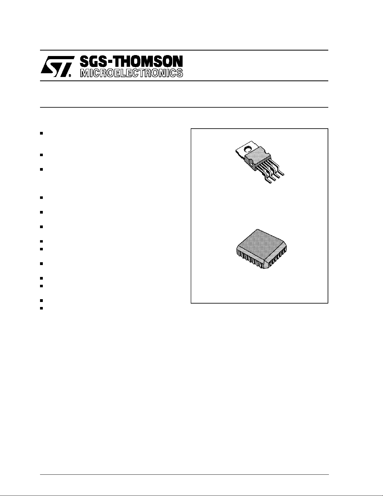
L3234
L3235
HEPTAWATT
ORDERING NUMBER: L3234
PLCC28
ORDERING NUMBER: L3235
injectorfabricatedin Bipolarin 140V Technology.
Its function is to amplify and inject in balanced
mode with zero crossing the ringing signal. The
DESCRIPTION
The L3234/L3235is a highly integrated SLIC KIT
targeted to PABX and key systemapplications
The kit integrates the majority of functions required to interface a telephone line. The
L3234/L3235implementsthe main featuresof the
broths function:
- Battery Feed (BalancedMode)
- Ringing Injection
- Signalling Detection
- Hybrid Function
The Kit comprises 2 devices, the L3234 ringing
Janauary 1995
This isadvanced information on a new product now in development or undergoing evaluation.Details are subject to change without notice.
device requires an external positive supply of
100V and a low level sinusoid of approx.
950mVrms. The L3235 Line Feeder is integrated
in 60V Bipolar Technology. The L3235 provides
batteryfeed tothe line with programmablecurrent
limitation. The two to four wire voice frequency
signal conversion is implemented by the L3235
and line terminating and balance impedancesare
externally programmable. The L3234/L3235kit is
designed for low power dissipation. In a short
loop conditionthe extrapower is dissipated on an
external transistor. The Kit is controlled by five
wire parallel bus and interfaces easily to all first
and programmable second generation COMBOS.
(seefigg. 1 and 2)
1/26

L3234 - L3235
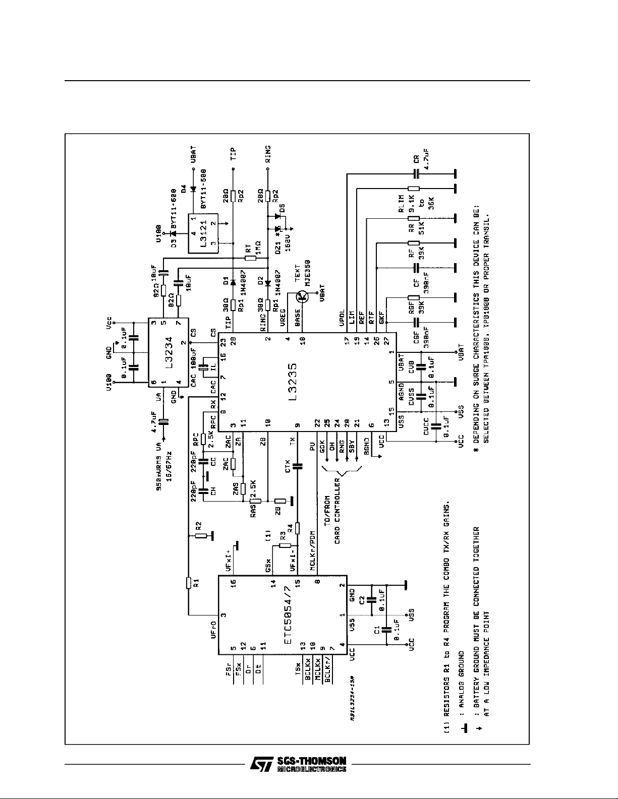
Figure1: Typical ApplicationCircuit with SecondGeneration COMBO for Complete Subscriber Circuit
(Protection-SLIC-COMBO)
2/26
L3234 - L3235
Figure2: Typical ApplicationCircuit with First GenerationCOMBO for Complete Subscriber Circuit
(Protection-SLIC-COMBO)
3/26

L3234 - L3235
L3234
Solid State Ringing Injector
DESCRIPTION
The L3234 is a monolithic integratedcircuit which
is part of a kit of solid state devices for the subscriber line interface. The L3234 sends a ringing
signal into a two wires analog telephone line in
balanced mode. The AC ringing signal amplitude
is up to 60Vrms, and for that purpose a positive
supply voltage of +100V shall be available on the
subscribercard.
The L3234 receives a low amplitude ringing signal (950mVrms) and provide the voltage/current
amplification (60Vrms/70mA) when the enable input is active (CS > 2V). In disable mode (CS <
0.8V) the power consumption of the chip is very
low (<14mW).
The circuit is designed with a highvoltage bipolar
technology(V
>140V / V
CEO
CBO
>250V).
HEPTAWATT
The packageis a moulded plastic power package
(Heptawatt)suitable also for surface mounting.
BLOCK DIAGRAM
4/26
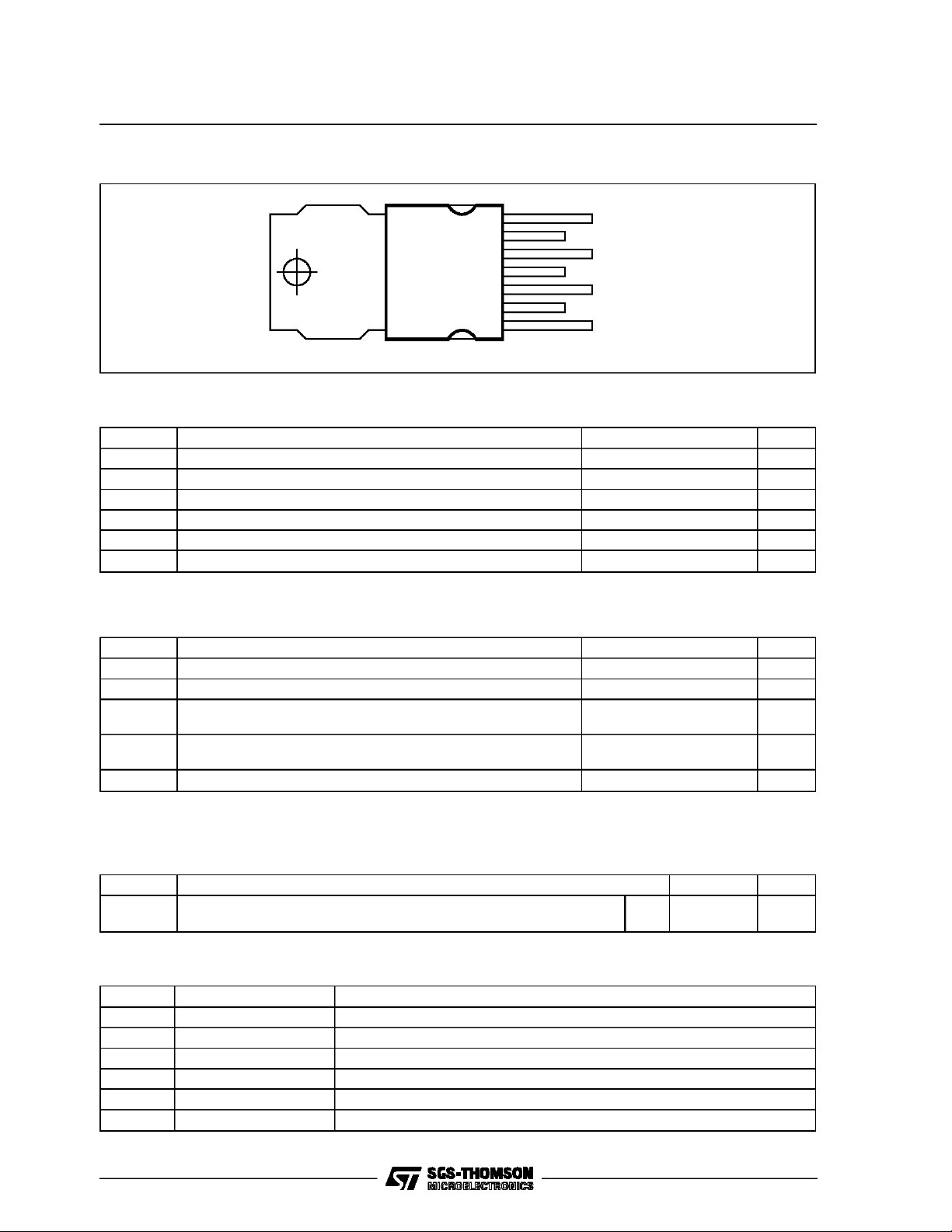
PIN CONNECTION (Top view)
L3234 - L3235
7
6
5
4
3
2
1
D94TL131
OUT2
V100
OUT1
GND
VCC
CS
VA
ABSOLUTE MAXIMUM RATINGS
Symbol Parameter Value Unit
V100 Positive Power SupplyVoltage +120 V
V
V
CS Logical Ring DriveInput V
T
T
5V Power Supply Voltage 5.5 V
CC
Low Voltage Ringing Signal (with V100 = 120Vdc) 1.4 Vrms
A
CC
Max. Junction Temperature 150
j
Storage Temperature -55 to +150
stg
OPERATINGRANGE
Symbol Parameter Value Unit
V100 High Power Supply Voltage 95 to 105 V
V
V
T
T
Low Power Supply Voltage 5 ±5% V
CC
Low Voltage Ringing Signal
A
Operating Temperature for L3234
op
Max. Junction Operating Temperature (due to thermal protection) 130 °C
jop
L3234T
600 to 950
within 10Hz -100Hz
0to70
-40 to 85
o
C
o
C
Vrms
°C
°C
Note: Operating ranges definethose limits between which the functionality ofthe device is guaranteed.
THERMAL DATA
Symbol Description Value Unit
R
th j-case
R
th j-amb
Thermal ResistanceJunction-case
Thermal ResistanceJunction-ambient
Max.
Max.
4
50
PIN DESCRIPTION
Pin Name Description
1 VA Low Voltage Ringing Signal Input
2 CS Logical Ring Drive Input
3V
CC
4 GND Common Analog-Digital Ground
5 OUT1 Ringing Signal Output
6 V100 +100V High Power Supply
+5V Low Power Supply
o
C/W
o
C/W
5/26

L3234 - L3235
OPERATIONDESCRIPTION
The Fig. 3 show the simplifiedcircuit configuration
Figure3: L3234/L3235Circuit Configuration
CO1
CO2
RO1
RO2
TIP
LINE TERMINALS
RING
LINE FEEDER
A
B
L3235
of the L3234 Solid State Ringing injector when
used with the L3235 Line Feeder.
+5VGND+100V
C100 CVCC
VCCGNDV100
643
CS
5
RINGING INJECTOR
7
L3234
2
CA
1
VA
VA
D94TL132
OUT1
OUT2
CS
GND
-VBAT
EXTERNALCOMPONENTSLIST
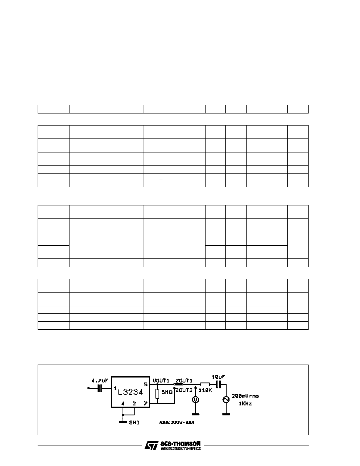
In the followingtable are shown the recommendedexternalcomponentsvalues for L3234.
Ref. Value Involved Parameter or Function
R01, R02 82Ω Ringing Feeding SeriesResistors
C01, C02 10µF - 160V Ringing Feeding Decoupling Capacitors
CA 4.7µF - 10V Low LevelRinging Signal De coupling Capacitor
C100 100nF - 100V Positive Battery Filter
CV
CC
When the ringing function is selected by the subscriber card, a low level signal is continuously applied to pin 1 througha de couplingcapacitor.Then
thelogicalringdrivesignalCS providedby L3235is
appliedto pin2 witha cadencedmode.
The ringing cycles are synchronised by the L3234
in such a way that the ringing starts and stops alwayswhenthe analoginputsignalcrosses zero.
When the ringing injection is enabled (CS = ”1”),
an AC ringing signal is injected in a balanced
6/26
100nF +5V Supply Filter
modeinto thetelephone line.
When the ringing injection is disabled (CS = ”0”),
the output voltage on OUT2 raises to the high
power supply, whereas on OUT1, it falls down to
ground.
The L3234 has a low output impedance when
sending the signal, and high output impedance
when the ringing signal is disabled
In fig. 4 the dynamic features of L3234 are
shown.
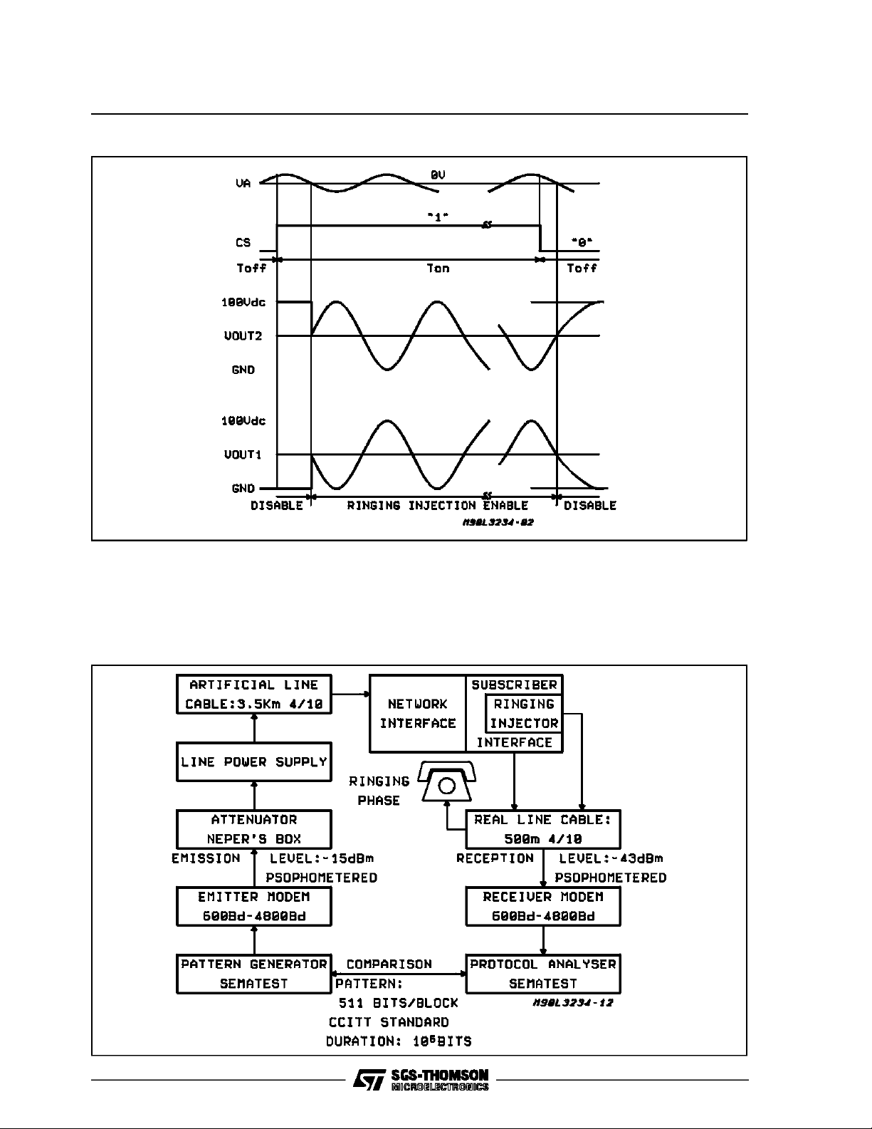
Figure4: Dynamic Features of L3234
L3234 - L3235
DATATRANSMISSION INTERFERENCE TEST
The L3234 meet the requirementsof the technical
specification ST/PAA/TPA/STP/1063 from the
CNET. The test circuit used is indicated below.
The measured error rate for data transmission is
lower than 10
This test measuresif during the ringing phase the
circuitinduce any noise to the closer lines.
Figure5: Test CircuitData TransmissionInterferenceTest
-6
during the ringing phase.
7/26
L3234 - L3235
ELECTRICAL CHARACTERISTICS (Test conditions:V100 = +100V,VCC= +5V, T
=25°C, unless oth-
amb
erwise specified)
Note: Testing of all parameteris performed at 25°C. Characterisation,as well as the design rule used al-
low correlation of tested performance with actual performances at other temperatures. All parameters listed here are met in the range 0°C to +70°C. For applications requiring operations in
the standard temperature range (0°Cto70°C) use L3234. If operations are required in the ex-
tended temperaturerange (-40°Cto85°C), use theL3234T.
Symbol Parameter Test Condition Min. Typ. Max. Unit Fig
STANDBY MODE: CS = ”0”
IS(V100)
I
S(VCC
V
SOUT1
V
SOUT2
Z
SOUT1
Z
SOUT2
THD Harmonic Distortion During
Consumption VA = 950mVrms; 50Hz 45
)
DC Output Voltage VA = 950mVrms; 50Hz
Output Impedance 70
Z
Matching 15 %
OUT
< 6dBm; f = 1kHz -46 -40 dB 7
V
LINE
Emission
92
70
560
100
800
µA
µA
6V
V
kΩ
kΩ
6
RINGINGPHASE: CS = ”1”
DC OPERATION
IR(V100)
I
)
R(VCC
V
ROUT1
V
ROUT2
V
IH
IIH(CS = 0)
V
IL
IIL(CS = 0)
I
lim
Consumption Z
DC Output Voltage VA = 0V 44
Threshold Voltage on the
Logical Input CS
DC Line Current Limitation VA = 0V 70 150 mA 12
= ∞
LINE
VA = 950mVrms; 50Hz
44
VA = 950mVrms; 50Hz 2.0
2.5
2.2
5
3
56
56
1
0.8
1
mA
mA
V
V
V
µA
V
µA
8
AC OPERATION
V
/VA
OUT1
V
/VA
OUT2
V
OUT1-VOUT1
Ringing Gain Z
Ringing Signal ZLINE = 2.2µF+1kΩ
= 2.2µF+1kΩ
LINE
VA = 0dBm
29.5
29.5
30
30
57 60 Vrms
VA = 950mVrms; 50Hz
THDV
(VA) InputImpedance VA = 950mVrms; 50Hz 40 kΩ 10
Z
IN
Z
OUT
Harmonic Distortion VA = 950mVrms; 50Hz 5 %
LINE
Differential Output Impedance I
< 50mArms 20 Ω 11
LINE
TEST CIRCUITS
Figure6.
8/26
dB
dB
9
9

TEST CIRCUITS (continued)
Figure7.
VCC V100
L3234 - L3235
Figure8.
4.7µF
CS
2
1
L3234
4
GND
D94TL133
VOUT2
63
7
VOUT1 A
5
82Ω
82Ω
10µF/160V
10µF/160V
-VBAT
LINE FEEDER
1MΩ
B
V
ZLINE=600Ω
VE 1KHz
Figure9.
9/26

L3234 - L3235
TEST CIRCUITS (continued)
Figure10.
Figure11.
Figure12.
10/26

L3235
Subscriber Line Interface Circuit
DESCRIPTION
Circuitdescription
The L3235 Subscriber Line Interface Circuit
(SLIC) is a bipolar integrated circuit in 60V technologyoptimized for PABX application.
The L3235 supplies a line feed voltage with a current limitation which can be modified by an external resistor (RLIM).
The SLIC incorporates loop currents, ground key
detectionfunctionswith an externallyprogrammable constant time.
The two to four wires and four to two wires voice
frequency signal conversion is performed by the
L3235 and the line terminating and the balancing
impedancesare externallyprogrammable.
The device integrates an automatic power limitation circuit. In shortloop conditionthe extrapower
isdissipated on one external transistor (Text).
This aproach allows to assembly the L3235 in a
low cost standardplastic PLCC28 package.
The chip is protected by thermal protection at
Tj = 150°C.
The SLIC is able to givea powerup commandfor
Combo in off hook condition and an enable logic
for solidstate ringing injectorL3234.
The L3235 package is 28 pin plastic PLCC.
The L3235 has been designed to operate
togheter with L3234 performing complete
BORSHT function without any electromechanical
ringingrelay (see theapplication circuit fig. 16).
L3234 - L3235
PLCC28
PINCONNECTION
ABSOLUTE MAXIMUM RATINGS
Symbol Parameter Value Unit
V
BAT
V
CC
V
SS
T
T
stg
Battery Voltage -54 V
Positive Supply Voltage 5.5 V
Negative Supply Voltage -5.5 V
Max. Junction Temperature 150 °C
j
Storage Temperature -55 to +150 °C
OPERATINGRANGE
Symbol Parameter Min. Max. Unit
V
BAT
V
CC
V
SS
T
op
T
Note: Operating ranges definethose limits between which the functionality ofthe device is guaranteed.
Battery Voltage -52 -24 V
Positive Supply Voltage 4.75 5.25 V
Negative Supply Voltage -5.25 -4.75 V
Operating Temperature for L3235
Max Junction Operating Temperature 130 °C
j
L3235T
0
-40
70
85
°C
°C
11/26

L3234 - L3235
THERMAL DATA
Symbol Description Value Unit
R
th j-amb
PIN DESCRIPTION
Pin Name Description
1V
2 RING RING wire of 2 Wire LineInterface.
3 ZAC Non Inverting Inputof the AC Impedance Synthesis Circuit.
4 VREG Emitter Connection for the External Transistor.
5 AGND Analog/Digital Ground.
6 BGND Battery Ground. This is the Reference for the Battery Voltage (note 1).
7 CAC AC Current Feedback Input.
8 RPC External Protection Resistors AC TransmissionCompensation.
9 TX Four Wire Transmitting Amplifier Output.
10 ZB NonInverting OperationalInput Inserted in the Hybrid Circuit for 2W to 4W
11 ZA VRXOutput Buffer 2W to 4W Conversion.
12 RX High Impedance Four WireReceiving Input.
13 V
14 REF Voltage Reference Output; a Resistor Connected to this pin sets the Internal
15 V
16 IL Transversal Line Current Feedback Divided by 50.
17 VPOL Non Inverting OperationalInput to Implement DC Character.
18 BASE Driver for ExternalTransistor Base.
19 LIM Voltage Reference Output; a Resistor Connected to this Pin Sets the Value of
20 RNG Ringing Logic Input from Line Card Controller.
21 SBY Stand byLogic Input(SBY = 1 Set Line Current Limitation at 3mA).
22 PU Power u.p Logic Output forthe CodecFilter. (PU = 0 means CodecFilter
23 CS Ring Injector Enable for L3234 Output. (CS= 1 means L3234 Ringing
24 OH Hook Status Logic Output (OH = 0 means off hook).
25 GDK Ground Key Status Logic Output (GDK = 0 means Ground Key on).
26 RTF Time Constant Hook Detector Filter Input.
27 GKF Time Constant GK Detector FilterInput.
28 TIP Tip Wire of 2 Wire Line Interface.
Note 1:
AGND and BGND pins must betied together at a low impedance point (e.g. at card connector level).
Thermal ResistanceJunction-ambient Max 80 °C/W
bat
Negative Battery Supply Input.
Conversion. The Network Connected from this Pinto Ground shall be a copy
of the Line Impedance.
CC
Positive 5V Supply Voltage.
Bias Current.
SS
Negative 5V Supply Voltage.
Line Current Limitation.
Activated)
Injection Enable).
12/26

L3235FUNCTIONAL DIAGRAM
L3234 - L3235
FUNCTIONAL DESCRIPTION
DIGITALINTERFACE
The different operating modes of the L3235 are
programmed through a digital interface based on
two input pins:
1)SBY input programs the stand-by or Active/Ringingmodes.
2)RNGinput programs theringing ON/OFF activationcondition for the L3234.
The L3235 digital interface has four outputpins :
1)OH provides the on hook/offhook or ring trip
informations(active low).
2)GDK provides the ground key on/off information (active low).
3)PU must be connected to the enable input pin
of CODEC/FILTER devices like ETC 5054/57
and automatically activates this device when
in active mode off-hook is detected or when
ringingmode is selected.
4)CS output must be connected to the CS enable input of the solid state ringing injector
L3234.
In this way the L3234 will be enabled when ringing mode is programmed and will be automatically disabled when the ring trip condition will be
detected reducing the ringing signal disconnectiontime after ring trip.
The table 1 here below resumes the different operation modes and the relative logic output signals.
The two current detection (hook and GND key)
have internal fixedthreshold. Externally it is possible to program their time costant through two R-C
components connected respectively to pin 26
(RTF)and pin 27 (GKF).
13/26

L3234 - L3235
Table 1.
OPERATING
MODE
ACTIVE
RINGING
STAND-BY
(*)This status is latched and doesn’t change until RNG turn to 0
INPUT PIN LINE STATUS OUTPUT PIN
SBY RNG
0
0
0
0
0
0
0
0
1
1
0
0
0
0
1
1
1
1
0
1
0: ON HOOK
1: OFF HOOK
0
0
1
1
0
0
1
1
X
X
OPERATINGMODES
Stand-By(SBY = 1 and RNG = 0)
In Stand-By mode the L3235 limits the DC Loop
currentto 3 mA.
In this mode all the AC circuits are active and all
the AC characteristics are the same as in Active
Mode.
Also the two Line Current detectors (hook and
GND key) are active but due to the loop current
limited to 3 mA they will notbe activated.
This mode is useful in emergencycondition when
it is very important to limits the system power dissipation.
RingingMode (SBY= 0 and RNG = 1)
When ringing mode is selected ”CS” pin is set to
1 in order to activate the L3234 ringinginjector.
See L3234 for detailed description.
Ring trip is detectedby means of the same inter-
nal circuitry usedfor off-hookdetection.
An off-hook delay time lower than
1
⁄2F
RING
should
be selected.(see ext. components list).
When ring trip is detected ”CS” is automatically
set to ”0” allowing in this way a quick ringing disconnection.
After Ring trip detection the Card Controllermust
set the L3235 in active mode to remove the internal latching of the ”CS” information.
0: NO GND KEY
1: GND KEY ON
0
1
0
1
0
1
0
1
X
X
OH GDK PU CS
1
0
0
0
1
0
0
0
1
1
1
0
1
0
1
0
1
0
1
1
1
0
0
0
0
0
0
0
1
0
0
0
0
0
1
0(*)
0(*)
0(*)
0
1
Active mode (SBY = 0 and CS1 = 0)
In Active mode the L3235 has the DC charac-
teristic show in Fig.13
The DC characteristicsof L3235 has two different
feedingconditions:
1)Current Limiting Region : (short loop) the DC
impedance of the SLIC is very high (>20
Kohm) therefore the system works as a current generator.By the ext. resistor RLIM connected at pin 19 it is possible to programlimiting currentvalues from 20 mAto 70 mA.
2) Voltagesource region (long loop).
The DC impedance of the L3235 is almost
equal to zero therefore the systemworks like
a voltage generator with in series the two external protectionresistors Rp.
When a limiting current value higher than 40 mA
is programmed the device will automatically reduce to 40 mA the loop current for very short
loop.
This is done in order to limit the maximum power
dissipationin very short loop to values lower than
2W for the external transistor and lower than
0.5W for the L3235 itself.
This improve the system reliability reducing the
L3235 power dissipation and therefore the internal junction temperature.
14/26

L3234 - L3235
Figure13: DCcharacteristicin Active Mode withtwo different valuesoflimitingcurrent(30mAand70mA).
Figure14: Line current versus loop resistance with two differentvalues of limiting current (30mA and
70mA)
R
are the protection resistors
AC characteristic
A simplified AC model of the transmission circuits
is shown in figure 15.
Where :
Vrxis the received signal
V
is the transmitted signal
tx
V
is the AC transversal voltage at line terminations.
l
E
is the line open circuit AC voltage
g
Z
is the line impedance
l
p
Z
is the line impedance balancingnetwork
B
Z
is the SLIC impedance balancing network
A
Z
program the AC linetermination impedance
AC
R
used for external protection resistors insertion
PC
loss compensation
I
/50 is the AC transversal current divided by 50
l
CAC AC feedback current decoupling
15/26

L3234 - L3235
Figure15: SimplifiedAC Circuits
Two wire impedance
To calculate the impedance presented to the two
wire line by the SLIC including the protection resistorsR
V
rx
Il/50’= Il/50 (in first approximation)
Rp = 50Ω
Z
S=ZAC
ZACto make ZS=600Ω
Z
AC
Z
AC
Z
AC
Two wire to four wire gain (Txgain)
Let V
G
tx
V
tx
V
l
Example:Calculate Gtx making RPC=50⋅R
Gtx= 2 ⋅
As you can see the RPC resistor is providing the
compensation of the insertion loss introduced by
the two external protectionresistors R
Four wire to two wire gain (Rx gain)
Let Eg =0
G
rx
Example:
CalculateG
G
rx
and definedas ZSlet:
p
=0
/25 + 2R
P
=25•(ZS-2RP)
=25⋅(600- 100)
=12.5KΩ
=0
rx
V
tx
=
V
l
+ R
Z
=2⋅
AC
ZAC+ 50R
+ 50 ⋅ R
Z
AC
ZAC+ 50 ⋅ R
V
l
=
=
V
=
25 ⋅ (Z
25⋅ (Zl+ 2R
rx
makingZAC=25⋅(ZML-2⋅RP)
rx
50 ⋅ Z
+ 2R
l
P
PC
P
P
= 2
P
⋅ Z
50
P
l
− 2RP+ Z
l
)+ Z
ML
AC
P
.
P
)
2 ⋅ Z
Zl+ Z
l
ML
Grx=
In particular for ZS=Zl:Grx=1
Hybridfunction
To calculatedthe transhybridloss (Thl)let: Eg = 0
Thl =
= 4 (
Z
Z
B
+ ZA−
B
VT
x
=
VR
x
50 ⋅ ( 2 ⋅ R
50 ⋅ ( 2 ⋅ RP+ Zl)−2R
+ Zl)−2R
P
PC
AC
)
Example:
Calculating Thl making R
(ZSlic- 2 ⋅ R
Thl = 4 ⋅ (
In particular if
)
P
Z
B
Z
−
+ Z
B
Z
A
Z
Z
A
=
Z
Z
B
=50⋅RP,ZS=25⋅
S
Z
l
)
+ Z
l
ML
S
l
Thl = 0
From the above relation it is evident that if Z
equal to the Z
used in Thl test, the two ZA,ZBim-
l
S
pedancescan be tworesistorof the same value.
ACtransmissioncircuit stability
To ensure stability of the feedback loop shown in
blockdiagram form in figure 15 two capacitorsare
required. Figure 16 includes these capacitors Cc
and Ch.
AC - DCseparation
The high pass filter capacitor C
provides the
AC
separationbetweenDC circuitsand AC circuits.A
CAC value of 100mF will position the low end frequencyresponse 3dB break point at 7Hz,
fsp =
2π ⋅ 220Ω ⋅
1
C
AC
is
16/26

L3234 - L3235
Externalcomponents list forL3235
To set the SLIC into operation the followingparametershave to be defined:
- The AC SLICimpedance at line terminals ”Zs” to which the return loss measurementsis referred. It can
bereal (typ.600Ω)or complex.
- The equivalent AC impedanceof the line ”Zl”used for evaluationof the trans-hybridloss performance
(2/4 wire conversion).It is usually a compleximpedance.
- The value of the two protection resistorsRp inseries with the line termination.
Once, the above parameters are defined,it is possible to calculateall the external componentsusing the
followingtable. Thetypicalvalues has been obtained supposing:Zs = 600Ω; Zl =600Ω;Rp=50Ω
Name Suggested Value Function Formula
R
F
C
F
R
GF
C
GF
R
R
R
LIM
CR 4.7µF
R
P
R
T
C
AC
R
PC
Z
AC
C
C
Z
AS
R
AS
ZB 15K
C
H
C
TX
D1, D2 1N4007 Line Rectifier
Text (3) External Transistor P
;CV
CV
SS
DD
C
VB
Notes:
1) For proper operation Cf should be selected in order to verify the following conditions:
A)cf > 150nF
B)τ < 1/2 • f
f
RING
2) For protection purposes the RP resistor is usually splitted in twopart R
3) ex: BD140; MJE172; MJE350.... (SOT32 or SOT82 package availablealso for surface mount). For low power application (reduced battery
voltage) BCP53 (SOT223 surface mount package) can beused. Depending on application enviromentan heatsink could be necessary.
RING
: Ringing signal frequency
39KΩ
390nF
39KΩ
390nF
Delay Time
On-hook Off-hook
Delay Time
GK Detector
τ = 0.69 ⋅ C
τ = 0.69 ⋅ C
⋅ 39KΩ (1)
F
⋅ 39KΩ
GF
51KΩ Bias Set
8.4KΩ to 33KΩ Ext. Current Limit. Progr.
NegativeBattery
6.3 V 30%
Filter
R
LIM
C
AC
=
I
LIM
=
2π ⋅ 16KΩ ⋅
564
− 3mA
1
50 Protection Resistors 47 < RP< 100Ω (2)
1MΩ 20% TerminationResistor
100µF
6.3V 20%
DC/AC current feedbacksplitting
C
AC
=
2π ⋅ 220Ω ⋅
1
2500Ω 1% RPinsertionloss compensation RPC=25⋅(2RP)
12500Ω 1% 2W AC Impedance programmation ZAC=25⋅(ZS-2RP)
220pF 20% AC Feedback compensation
f1 = 300KHz C
=
C
2πf1 ⋅ 50R
12500Ω 1% Slic Impedance Balancing Net. ZAS=25⋅(ZS-2RP)
2500Ω 1% RAS = 25 ⋅ (2RP)
1% Line impedance Balancing Net. ZB=25⋅Zl
Ω
220pF 20% CCTransybrid loss Compensation
4.7µF 30% DC Decoupling Tx Output
C
H=CC
C
=
TX
> 2W, V
Diss
H
> 40, IC> 100mA
FE
V
< 0.8V@ 100mA
BE
Z
AC
⋅
Z
AS
1
6.28 ⋅ fp ⋅ Z
CEO
100nF ±5V supply filter
100nF/100V V
supply filter
BAT
and RP2, with RP1>30Ω.
P1
fp
f
sp
load
> 60V
1
P
17/26

L3234 - L3235
Figure16: TypicalAppicationCircuit Including L3234 andProtection
18/26

L3234 - L3235
ELECTRICAL CHARACTERISTICS (Test condition:refer to the test circuitof the fig. 17; VCC= 5V,
= -5V, V
V
SS
Note: Testing of all parameters is performed at 25°C. Characterization,as well as the designrules used
allow correlation of tested performance with actual performance at other temperatures. All parameters listed here are met in the range 0°C to +70°C. For applications requiring operations in
the standard temperature range (0°Cto70°C) use L3234. If operations are required in the ex-
tended temperaturerange (-40°Cto85°C), use theL3234T.
Symbol Parameter Test Condition Min. Typ. Max. Unit Fig.
STAND-BY
V
ls
I
LCC
DC OPERATION
= -48V, T
bat
Output Voltage atTIP/RING
=25°C, unlessotherwisespecified)
amb
I
= 0 35.7 39 V
LINE
pins
Short Circuit Current Stand-by, SBY = 1 2 3 4 mA
V
lP
I
lim
I
lim
I
O
I
f
I
lgk
Gklim Ground Key Current
Output Voltage at TIP/RING
pins
Current Progr. I
Current Progr. 8.4KΩ <R
I
=0
LINE
I
= 50mA
LINE
Prog. = 70mA 63 70 77 mA
lim
< 33KΩ 20 70 mA
LIM
35.7
35.2
39
39
On-hook Threshold 5
Off-hook Threshold 10
GK Detector Threshold 10 17
RING to BGND 13 22 mA
Limitation
Gkov Ground Key Threshold
Gklim-Ilgk 1 mA
Overloap
I
max
Max. Output Current at
I
= 70mA 90 140 mA
lim
TIP/RING
IV
IV
IV
CC
SS
bat
Supply Current from V
Supply Current from V
Supply Current from V
CC
SS
bat
I
= 0 6.2 8 mA
line
Iline = 0 1.6 2.1 mA
Iline = 0 2.8 3.6 mA
AC OPERATION
Z
tx
Z
rx
R
l
Thl Trans Hybrid Loos f = 300 to 3400Hz 20 36 dB A2
G
s
G
sf
G
sl
G
r
G
rf
G
rl
Np4W Psoph. Noise atTx -69 -62 dBmp
Np2W Psoph. Noise at Line -75 -68 dBmp
S
vrr
S
vrr
L
tc
T
lc
(*) Selected parts L3235C
Sending Output Impedance pin 9 (Tx) 10 Ω
Receiving Input Impedance pin 12 (Rx) 1 MΩ
2W Return Loss f = 300 to 3400Hz 20 36 dB A1
Sending Gain f = 1020Hz Il= 20mA 5.82 6.02 6.22 dB A3
Flatness f = 300 to 3400Hz -0.2 0.2 dB
Linearity -20dB to 10dBm -0.2 0.2 dB
Receiving Gain f = 1020Hz Il= 20mA 0.2 0 0.2 dB A4
Flatness f = 300 to 3400Hz -0.2 0.2 dB
Linearity -20dBm to +4dBm -0.2 0.2 dB
Relative to V
Terminal versus Tx Terminal
Relative to Vccand V
versus Line Terminal versus
versus Line
bat
f = 1020Hz
V
= 100mVpp
S
ss
f = 1020Hz
V
= 100mVpp
S
-30
-24
-20
-14
Tx Terminal
L/T Conversion measured at
line Terminals
T/L Conversion Measured at
Line Terminals
f = 300 to 3400
I
= 20mA
line
f = 300 to 3400
I
= 20mA
line
49
53(*)
46(*) dB A7
V
V
dB
dB
dB
dB
dB
dB
A5
A6
19/26

L3234 - L3235
ELECTRICAL CHARACTERISTICS (continued)
Symbol Parameter Test Condition Min. Typ. Max. Unit Fig.
DIGITALSTATIC INTERFACE
V
il
V
ih
I
il
I
ih
V
ol
V
oh
Input Voltage at Logical ”0” Input SBY, CS1 0 0.8 V
Input Voltage at Logical ”1” Input SBY, CS1 2 5 V
Input Current at Logical ”0” Input SBY, CS1 10 µA
Input Current at Logical ”1” Input SBY, CS1 10 µA
Output Voltage at Logical ”0” I
Output Voltage at Logical ”1” I
Figure17: Test Circuit
out
I
out
out
I
out
= 1mA
=10µA
=10µA
= 1mA
4
2.7
0.5
0.4
V
V
V
V
20/26

L3234 - L3235
APPENDIXA
L3235 TEST CIRCUITS
Referring to the test circuit reported in fig 17 you
can find the proper configuration for the main
measurements.
FigureA1: 2W Return Loss
100µF
100µF
|Z
− Z|
R
L
= 20 log
ML
|ZML+ Z|
In particular:
A-B: Line terminals
C: Tx sending output on 4Wside
D: Rx receiving input on 4W Side
|2V
|
=20 log
|E
S
|
FigureA2: Trans-hybridLoss
V
T
HL
=20log
S
V
R
FigureA3: SendingGain
100µF
100µF
100µF
100µF
21/26

L3234 - L3235
TEST CIRCUITS(continued)
FigureA4: ReceivingGain
100µF
100µF
FigureA5: SVRRRelative to Battery Voltage VB
100µF
100µF
FigureA6: Longitudinalto TransversalConversion
22/26

FigureA7: Transversalto LongitudinalConversion
L3234 - L3235
APPENDIXB
LAYOUTSUGGESTIONS
Standard layout rules should be followed in order
to get thebest systemperformances:
1)Use always 100nF filtering capacitor close to
thesupply pins of each IC.
2) TheL3235biasresis tor(RR)shouldbeconnected
close to the correspondingpins ofL3235
(REFand AGND).
23/26

L3234 - L3235
HEPTAWATT (Surface Mount)PACKAGE MECHANICAL DATA
DIM.
MIN. TYP. MAX. MIN. TYP. MAX.
A 4.8 0.189
C 1.37 0.054
D 2.4 2.8 0.094 0.110
D1 1.2 1.35 0.047 0.053
E 0.35 0.55 0.014 0.022
F 0.6 0.8 0.024 0.031
F1 0.9 0.035
G 2.41 2.54 2.67 0.095 0.100 0.105
G1 4.91 5.08 5.21 0.193 0.200 0.205
G2 7.49 7.62 7.8 0.295 0.300 0.307
H2 9.2 10.4 0.362 0.409
H3 10.05 10.4 0.396 0.409
L 4.6 5.05 0.181 0.198
L1 3.9 4.1 4.3 0.153 0.161 0.170
L2 6.55 6.75 6.95 0.253 0.265 0.273
L3 5.9 6.1 6.3 0.232 0.240 0.248
L5 2.6 2.8 3 0.102 0.110 0.118
L6 15.1 15.8 0.594 0.622
L7 6 6.6 0.236 0.260
M 0.17 0.32 0.007 0.012
V2 8°(max)
Dia 3.65 3.85 0.144 0.152
mm inch
24/26

PLCC28PACKAGE MECHANICAL DATA
L3234 - L3235
DIM.
MIN. TYP. MAX. MIN. TYP. MAX.
A 12.32 12.57 0.485 0.495
B 11.43 11.58 0.450 0.456
D 4.2 4.57 0.165 0.180
D1 2.29 3.04 0.090 0.120
D2 0.51 0.020
E 9.91 10.92 0.390 0.430
e 1.27 0.050
e3 7.62 0.300
F 0.46 0.018
F1 0.71 0.028
G 0.101 0.004
M 1.24 0.049
M1 1.143 0.045
mm inch
25/26

L3234 - L3235
Information furnished is believed to be accurate and reliable. However, SGS-THOMSON Microelectronics assumes no responsibility for the
consequences of use of such informationnor forany infringement ofpatents or other rights of third parties which may result from itsuse. No
license is granted by implication or otherwise under any patent or patent rights of SGS-THOMSON Microelectronics. Specifications mentioned in this publication are subject to change without notice. This publication supersedes and replaces all information previously supplied.
SGS-THOMSON Microelectronics products are not authorized for use as critical components in life support devices or systems withoutexpress writtenapproval of SGS-THOMSON Microelectronics.
1995 SGS-THOMSON Microelectronics - All RightsReserved
SGS-THOMSON Microelectronics GROUP OF COMPANIES
Australia - Brazil- France - Germany - Hong Kong - Italy - Japan - Korea -Malaysia - Malta - Morocco - The Netherlands- Singapore -
Spain - Sweden - Switzerland - Taiwan - Thaliand - United Kingdom - U.S.A.
26/26
 Loading...