

Page 1
®
.
OPERATING SUPPLY VOLTAGE UP TO 46 V
.
TOTAL DC CURREN T UP TO 4 A
.
LOW SATURATION VO LTAGE
.
OVERTEMPERATU RE P ROT ECTION
.
LOGICAL "0" INPUT VOLTAGE UP TO 1.5 V
(HIGH NOISE IMMUNITY)
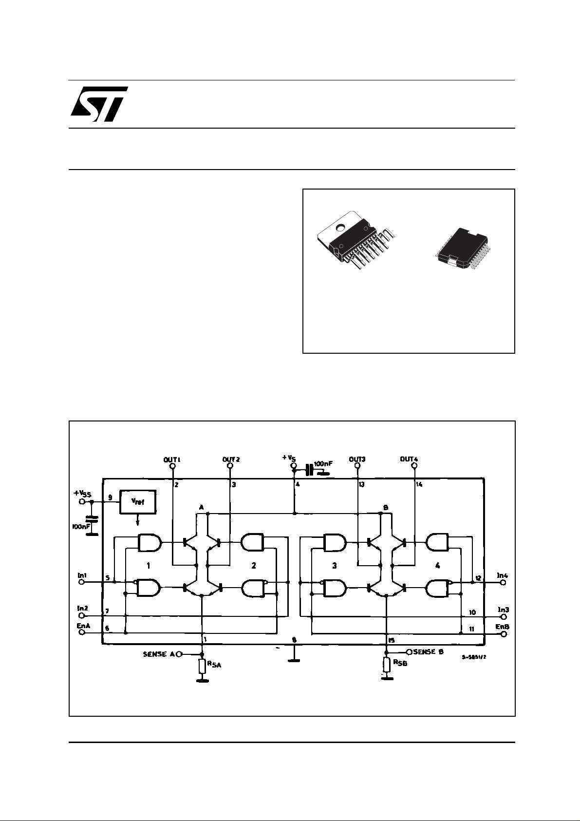
L298
DUAL FULL-BRIDGE DRIVER
DESCRIPTION
The L298 is an integrat ed m onolithic c irc uit in a 15 lead Multiwatt and PowerSO20 packages. It is a
high volt age , hig h c urrent dual f ul l-b ri dge driver designed to acc ept standard T TL logic lev els and drive
inductive loads such as relays, solenoids, DC and
stepping mot ors. Two enab le inputs are provided to
enable or di sable the d evice indepen dently of th e input signals. The emitters of the lower transistors of
each bridge are connected together and the corresponding e xte rnal termi nal c an b e us ed f or the co n-
BLOCK DIAGRAM
Multiwatt15
ORDERING NUMBERS :
L298HN (Multiwatt Horiz.)
L298P (PowerSO20)
nection of an external sensing r esistor. An ad ditional
supply in put is p ro vi ded so that the logic wor k s at a
lower voltage.
PowerSO20
L298N (Multiwatt Vert.)
Jenuary 2000
1/13
Page 2
L298
ABSOLUTE MAXIMUM RATINGS
Symbol Parameter Value Unit
V
V
SS
V
I,Ven
I
O
V
sens
P
T
op
T
stg
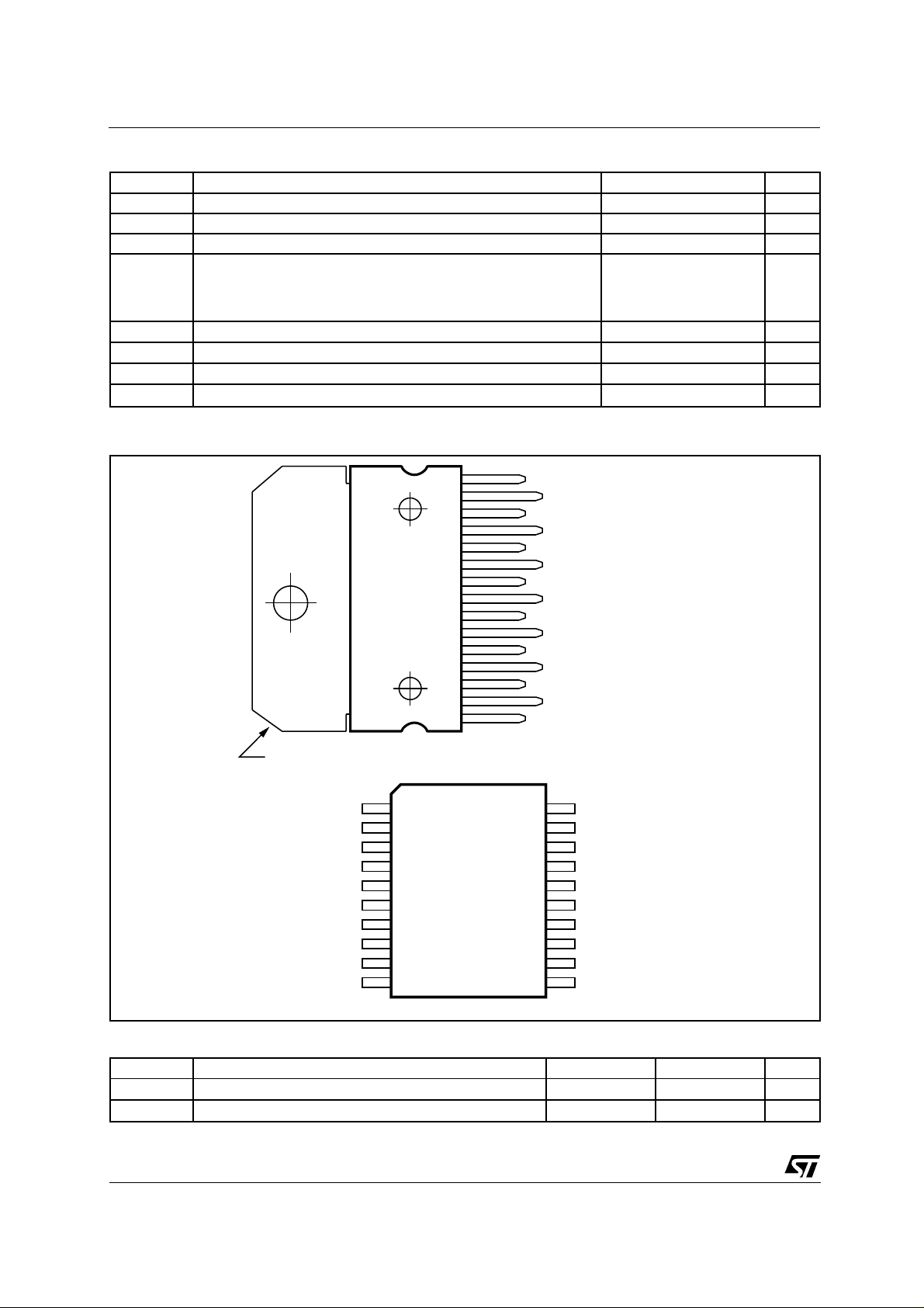
PIN CONNECTIONS (top view)
Power Supply 50 V
S
Logic Supply Voltage 7 V
Input and Enable Voltage –0.3 to 7 V
Peak Output Current (each Channel)
– Non Repetitive (t = 100µs)
–Repetitive (80% on –20% off; t
–DC Opera tio n
= 10ms)
on
3
2.5
2
Sensing Voltage –1 to 2.3 V
Total Power Dissipation (T
tot
case
= 75°C)
25 W
Juncti on Op era ting Temper at ur e –25 to 130
, TjStorag e and Junctio n Temp er atu re –40 to 150
A
A
A
C
°
C
°
Multiwatt15
TAB CONNECTED TO PIN 8
GND
Sense A
N.C.
Out 1
Out 2
V
S
Input 1
Enable A
Input 2
GND 10
1
2
3
4
PowerSO20
5
6
7
8
9
15
14
13
12
11
10
9
8
7
6
5
4
3
2
1
D95IN239
D95IN240A
20
19
18
17
16
15
14
13
12
11
CURRENT SENSING B
OUTPUT 4
OUTPUT 3
INPUT 4
ENABLE B
INPUT 3
LOGIC SUPPLY VOLTAGE V
GND
INPUT 2
ENABLE A
INPUT 1
SUPPLY VOLTAGE V
OUTPUT 2
OUTPUT 1
CURRENT SENSING A
GND
Sense B
N.C.
Out 4
Out 3
Input 4
Enable B
Input 3
VSS
GND
S
SS
THERMAL DATA
Symbol Parameter PowerSO20 Multiwatt15 Unit
R
th j-case
R
th j-amb
(*) Mounted on aluminum s ubst rate
2/13
Thermal Resistance Junction-case Max. – 3
Thermal Resistance Junction-ambient Max. 13 (*) 35
C/W
°
C/W
°
Page 3
PIN FUNCTIONS (refer t o the block diagram )
MW.15 PowerSO Name Function
1;15 2;19 Sense A; Sense B Between this pin and ground is connected the sense resistor to
control the current of the load.
2;3 4;5 Out 1; Out 2 Outputs of the Bridge A; the current that flows through the load
connected betw een these two pi ns is mon it or ed at pi n 1.
46 V
S
5;7 7;9 Input 1; Input 2 TTL Compatible Inputs of the Bridge A.
6;11 8;14 Enable A; Enable B TTL Compatible Enable Input: the L state disables the bridge A
8 1,10,11,20 GND Ground.
9 12 VSS Supply Voltage for the Logic Blocks. A100nF capacitor must be
10; 12 13;15 Input 3; Input 4 TTL Compatible Inputs of the Bridge B.
13; 14 16;17 Out 3; Out 4 Outputs of the Bridge B. The current that flows through the load
– 3;18 N.C. Not Connected
Supply Voltage for the Power Output Stages.
A non-inductive 100nF capacitor must be connected between this
pin and grou nd.
(enable A) and/or the bridge B (enable B).
connected between this pin and ground.
connected betw een these two pi ns is mon it or ed at pi n 15.
L298
ELECT RICAL CHARA CTE RISTICS (V
= 42V; VSS = 5V, Tj = 25°C; unless otherwise spec if ie d)
S
Symbol Parameter Test Conditions Min. Typ. Max. Unit
Supply Voltage (pin 4) Operative Condition VIH +2.5 46 V
V
S
V
Logic Supply Voltage (pin 9) 4.5 5 7 V
SS
I
Quiescent Supply Current (pin 4) Ven = H; IL = 0 Vi = L
S
V
= H
i
13
50
22
70
Ven = L Vi = X 4 mA
I
Quiescent Current from VSS (pin 9) Ven = H; IL = 0 Vi = L
SS
V
= H
i
24
7
36
12
Ven = L Vi = X 6 mA
V
Input Low Voltage
iL
–0.3 1.5 V
(pins 5, 7, 10, 12)
Input High Vol ta ge
V
iH
2.3 VSS V
(pins 5, 7, 10, 12)
Low Voltage Input Current
I
iL
Vi = L –10
(pins 5, 7, 10, 12)
High Voltage Input Current
I
iH
Vi = H ≤ V
–0.6V
SS
30 100
(pins 5, 7, 10, 12)
V
= L Enable Low Voltage (pins 6, 11) –0.3 1.5 V
en
= H Enable High Voltage (pins 6, 11) 2.3 V
V
en
Ien = L Low Voltage Enable Current
Ven = L –10
SS
(pins 6, 11)
= H High Voltage Enable Current
I
en
= H ≤ VSS –0.6V
V
en
30 100
(pins 6, 11)
V
CEsat (H)
V
CEsat (L )
V
CEsat
V
sens
Source Saturation Voltage IL = 1A
= 2A
I
L
Sink Saturation Voltage IL = 1A (5)
= 2A (5)
I
L
Total Drop IL = 1A (5)
= 2A (5)
I
L
Sensing Voltage (pins 1, 15) –1 (1) 2 V
0.95 1.35
2
0.85 1.2
1.7
1.7
2.7
1.6
2.3
1.80 3.2
4.9
mA
mA
mA
mA
µ
µ
V
µ
µ
V
V
V
V
V
V
A
A
A
A
3/13
Page 4
L298
ELECT RICAL CHARA CTE RISTICS (continued)
Symbol Parameter Test Conditions Min. Typ. Max. Unit
T
(Vi) Source Current Turn-off Delay 0.5 Vi to 0.9 IL (2); (4) 1.5
1
(Vi) Source Current Fall Time 0.9 IL to 0.1 IL (2); (4) 0.2
T
2
(Vi) Source Current Turn-on Delay 0.5 Vi to 0.1 IL (2); (4) 2
T
3
(Vi) Source Current Rise Time 0.1 IL to 0.9 IL (2); (4) 0.7
T
4
(Vi) Sink Current Turn-off Delay 0.5 Vi to 0.9 IL (3); (4) 0.7
T
5
(Vi) Sink Current Fall Time 0.9 IL to 0.1 IL (3); (4) 0.25
T
6
(Vi) Sink Current Turn-on Delay 0.5 Vi to 0.9 IL (3); (4) 1.6
T
7
(Vi) Sink Current Rise Time 0.1 IL to 0.9 IL (3); (4) 0.2
T
8
) Commutation Fre qu enc y IL = 2A 25 40 KHz
fc (V
i
T
(Ven) Source Current Turn-off Delay 0.5 Ven to 0.9 IL (2); (4) 3
1
(Ven) Source Current Fall Time 0.9 IL to 0.1 IL (2); (4) 1
T
2
(Ven) Source Current Turn-on Delay 0.5 Ven to 0.1 IL (2); (4) 0.3
T
3
(Ven) Source Current Rise Time 0.1 IL to 0.9 IL (2); (4) 0.4
T
4
(Ven) Sink Current Turn-off Delay 0.5 Ven to 0.9 IL (3); (4) 2.2
T
5
(Ven) Sink Current Fall Time 0.9 IL to 0.1 IL (3); (4) 0.35
T
6
(Ven) Sink Current Turn-on Delay 0.5 Ven to 0.9 IL (3); (4) 0.25
T
7
(Ven) Sink Current Rise Time 0.1 IL to 0.9 IL (3); (4) 0.1
T
8
s
µ
s
µ
s
µ
s
µ
s
µ
s
µ
s
µ
s
µ
s
µ
s
µ
s
µ
s
µ
s
µ
s
µ
s
µ
s
µ
1) 1)Sensing voltage c an be – 1 V for t ≤ 50 µsec; in stead y state V
2) See fig. 2.
3) See fig. 4.
4) The load must be a pure resistor.
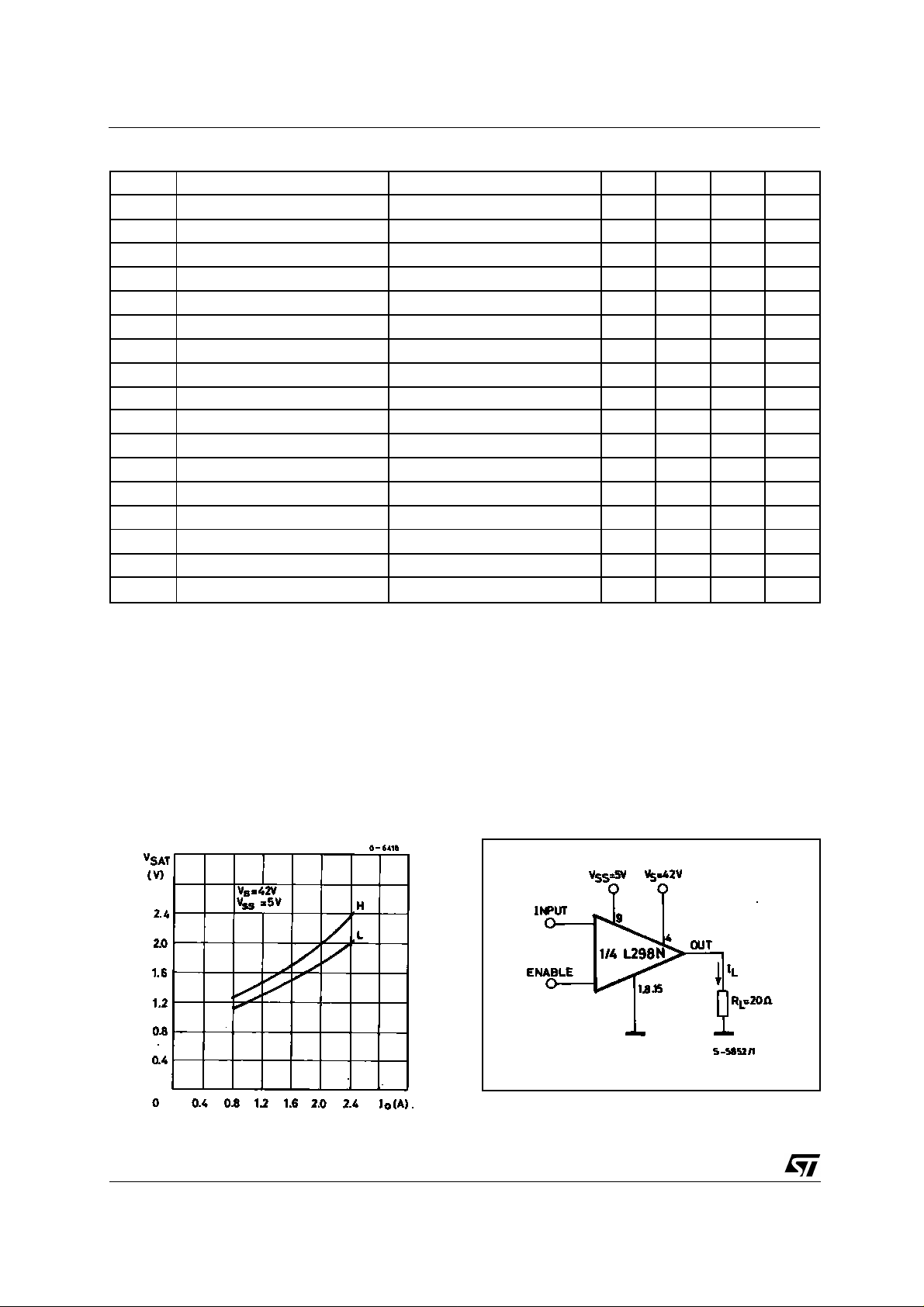
Figure 1 : Typical Sat ur ation Voltage vs . O utput
Current.
min ≥ – 0.5 V.
sens
Figure 2 : Switchin g Tim es T es t Cir c uit s .
4/13
Note :
For INPUT Switching, set EN = H
For ENABLE Switching, set IN = H
Page 5

Figure 3 : Source Cur ren t Delay Times vs. Input or En abl e S wit c hi ng.
Figure 4 : Switchin g Tim es T es t Cir c uit s .
L298
Note :
For INPUT Switching, set EN = H
For ENABLE Switching, set IN = L
5/13
Page 6

L298
Figure 5 : Sink Curre nt Delay Times vs. Input 0 V E nab le S witching.
Figure 6 : Bidirectional DC Motor C ont r ol.
Inputs Function
= H C = H ; D = L Forward
V
en
C = L ; D = H Reverse
C = D Fast Motor Stop
Ven = L C = X ; D = X Free Running
L = Low H = High X = Don’t care
Motor Stop
6/13
Page 7

L298
Figure 7 : For higher cur ren t s, ou tp uts can be par alleled. Tak e c ar e to par al lel c hannel 1 with cha nnel 4
and channel 2 wit h cha nnel 3.
APPLICATION INFORMATION (Re fer to the block diagra m)
1.1. POW ER OUTPUT ST A GE
The L298 in tegrates two pow er output stages (A ; B).
The power output stage is a bridge configuration
and its outputs can drive an inductive load in common or diffe renzial mo de, depend ing on the s tate of
the inputs. The current that flows through the load
comes out from the brid ge at the sen se out put : an
external r esis tor ( R
; RSB.) allows t o dete ct the in-
SA
tensity of this cu rr en t.
1.2. INPUT STAGE
Each bri dge is dri ven b y means of four gate s the in-
put of which ar e In1 ; In2 ; EnA a nd I n3 ; In4 ; E nB .
The In inputs s et the bridge st ate when The En i nput
is high ; a low state of t he En input inhibits the b ridge.
All the inpu ts ar e TT L com pa t ible .
2. SUGGESTIONS
A non inductive capacitor, usually of 100 nF, must
be foreseen between both Vs and Vss, to ground,
as near as pos sibl e to G ND pin. When the lar ge c apacitor of the powe r su ppl y is too f ar from the I C, a
second smaller one must be foreseen near the
L298.
The sense resi sto r, not of a wire wo und type, must
be grounded near t he ne gative pol e of V s that mu st
be near the GN D pin of the I.C.
Each input must be connected to the source of the
driving s ign als by me ans of a v er y shor t path.
Turn-On and Turn-Off : Before to Turn-ON the Supply Voltage and b efore to Turn it OFF, the E nable input must be d riven to the Low state.
3. APPLICATIONS
Fig 6 sho ws a bidirectional DC motor c ontr ol Sche-
matic Dia gram for wh ich o nly o ne bridg e is needed .
The external bridge of diodes D1 to D4 is made by
four fast recovery elements (trr ≤ 200 nsec) that
must be chosen of a VF as low as possible at the
worst cas e of t he lo ad c ur re nt .
The sen se output v oltage can be used to control the
current am plitude by chopp ing the inputs, or to provide ove rcurr ent p rotectio n by switc hing low the enable input.
The brake function (Fast motor stop) requires that
the Absolute Maximum Rating of 2 Amps must
never be ov er co m e.
When the repetitive peak current needed from the
load is higher than 2 Amp s , a p ar all eled configur ation can be chosen (See Fig.7).
An external bridge of diodes are required when inductive loads are dr iv en and whe n the inputs of the
IC are chop ped ; Sho ttky diodes would be preferred.
7/13
Page 8

L298
This solut ion can drive unt il 3 Amps In DC operati on
and until 3.5 Am p s of a r epetitive pea k cur r ent .
On Fig 8 it is shown the d riving of a two pha se bipolar
stepper motor ; the needed signals to drive the inputs of the L298 are generated, in this example,
from the IC L297.
Fig 9 show s an ex am ple of P.C.B . designed for the
applicati on of F ig 8.
Figure 8 : Two Phase Bipolar Stepp er Motor Circuit .
This circ uit dr iv es bipolar steppe r m otor s wit h w inding current s up to 2 A . The diodes are fas t 2 A types .
Fig 10 shows a second two phase bipolar stepper
motor control circuit where the current is controlled
by the I.C. L65 06.
RS1 = RS2 = 0.5
D1 to D8 = 2 A Fast diodes
8/13
Ω
VF ≤ 1.2 V @ I = 2 A
{
trr ≤ 200 ns
Page 9

Figure 9 : Suggested Pr int ed Cir c uit B oar d La y out for the Circuit of fi g. 8 (1 : 1 scale).
L298
Figure 10 : Two Phase Bi polar Stepper Mo tor C ont r ol C ir cu it by Us ing t he Cur re nt Con t rol ler L65 06.
RR and R
depend from the load current
sense
9/13
Page 10

L298
DIM.
MIN. TYP. MAX. MIN. TYP. MAX.
A 5 0.197
B 2.65 0.104
C 1.6 0.063
D 1 0.039
E 0.49 0.55 0.019 0.022
F 0.66 0.75 0.026 0.030
G 1.02 1.27 1.52 0.040 0.050 0.060
G1 17.53 17.78 18.03 0.690 0.700 0.710
H1 19.6 0.772
H2 20.2 0.795
L 21.9 22.2 22.5 0.862 0.874 0.886
L1 21.7 22.1 22.5 0.854 0.870 0.886
L2 17.65 18.1 0.695 0.713
L3 17.25 17.5 17.75 0.679 0.689 0.699
L4 10.3 10.7 10.9 0.406 0.421 0.429
L7 2.65 2.9 0.104 0.114
M 4.25 4.55 4.85 0.167 0.179 0.191
M1 4.63 5.08 5.53 0.182 0.200 0.218
S 1.9 2.6 0.075 0.102
S1 1.9 2.6 0.075 0.102
Dia1 3.65 3 .85 0.144 0.152
mm inch
OUTLINE AND
MECHANICAL DATA
Multiwatt15 V
10/13
Page 11

L298
DIM.
MIN. TYP. MAX. MIN. TYP. MAX.
A 5 0.197
B 2.65 0.104
C 1.6 0.063
E 0.49 0.55 0.019 0.022
F 0.66 0.75 0.026 0.030
G 1.14 1.27 1.4 0.045 0.050 0.055
G1 17.57 17.78 17.91 0.692 0.700 0.705
H1 19.6 0.772
H2 20.2 0.795
L 20.57 0.810
L1 18.03 0.710
L2 2.54 0.100
L3 17.25 17.5 17.75 0.679 0.689 0.699
L4 10.3 10.7 10.9 0.406 0.421 0.429
L5 5.28 0.208
L6 2.38 0.094
L7 2.65 2.9 0.104 0.114
S 1.9 2.6 0.075 0.102
S1 1.9 2.6 0.075 0.102
Dia1 3.65 3.85 0.144 0.152
mm inch
OUTLINE AND
MECHANICAL DATA
Multiwatt15 H
11/13
Page 12

L298
DIM.
MIN. TYP. MAX. MIN. TYP. MAX.
mm inch
A 3.6 0.142
a1 0.1 0.3 0.004 0.012
a2 3.3 0.130
a3 0 0.1 0.000 0.004
b 0.4 0.53 0.016 0.021
c 0.23 0.32 0.009 0.013
D (1) 15.8 16 0.622 0.630
D1 9.4 9.8 0.370 0.386
E 13.9 14.5 0.547 0.570
e 1.27 0.050
e3 11.43 0.450
E1 (1) 10.9 11.1 0.429 0.437
E2 2.9 0.114
E3 5.8 6.2 0.228 0.244
G 0 0.1 0.000 0.004
H 15.5 15.9 0.610 0.626
h 1.1 0.043
L 0.8 1.1 0.031 0.043
N 10˚ (max.)
S
8˚ (max.)
T10 0.394
(1) "D and F" do not include mold flash or protrusions.
- Mold flash or protrusions shall not exceed 0.15 mm (0.006").
- Critical dimensions: "E", "G" and "a3"
OUTLINE AND
MECHANICAL DATA
JEDEC MO-166
PowerSO20
E2
h x 45
DETAIL B
BOTTOM VIEW
R
lead
a3
Gage Plane
E
DETAIL B
0.35
S
D1
L
c
a1
DETAIL A
slug
- C -
SEATING PLANE
GC
(COPLANARITY)
E3
NN
a2
A
b
DETAIL A
e3
H
D
T
1
e
1120
E1
10
PSO20MEC
12/13
Page 13

L298
Information furnished is believed to be accurate and reliable. However, STMicroelectronics assumes no responsibility for the consequences of us e of such inform ation nor for any infringement of patent s or other right s of third parties whic h may result from its use. No
license is granted by implication or otherwise under any patent or patent rights of STMicroelectronics. Specification mentioned in this
publication are subject to change without notice. This publication supersedes and replaces all information pr eviously supplied. STMicroelectronics products are not authorized for use as critical components in life support devices or systems without express wr itten
approval of STMicr oelectronic s.
Australia - Brazil - Chin a - Finl and - France - Ger many - H ong Kong - In dia - Ital y - Japan - Mal aysia - Malta - M orocco -
The ST logo is a regis tered tradem ark of STMic roelec tronics
© 2000 STMicroelec tronics – Printed in Ital y – All Ri ghts Reserv ed
STMicroelectronic s GROUP OF COM PANIES
Singapore - Spain - Swede n - Swi tzerland - U nited K ingdom - U. S.A.
http://www.st.co m
13/13
 Loading...