

Page 1
Very low drop voltage regulators with inhibit
Features
■ Very low dropout voltage (0.4 V)
■ Very low quiescent current (typ. 50 µA in OFF
mode, 500 µA in ON mode)
■ Output current up to 500 mA
■ Logic-controlled electronic shutdown
■ Output voltages of 1.5; 2.5; 3.3; 4; 5; 8 V
■ Internal current and thermal limit
■ Only 2.2 µF for stability
■ Available in ± 2 % accuracy at 25 °C
■ Supply voltage rejection: 70 db (typ.)
■ Temperature range: -40 to 125 °C
Description
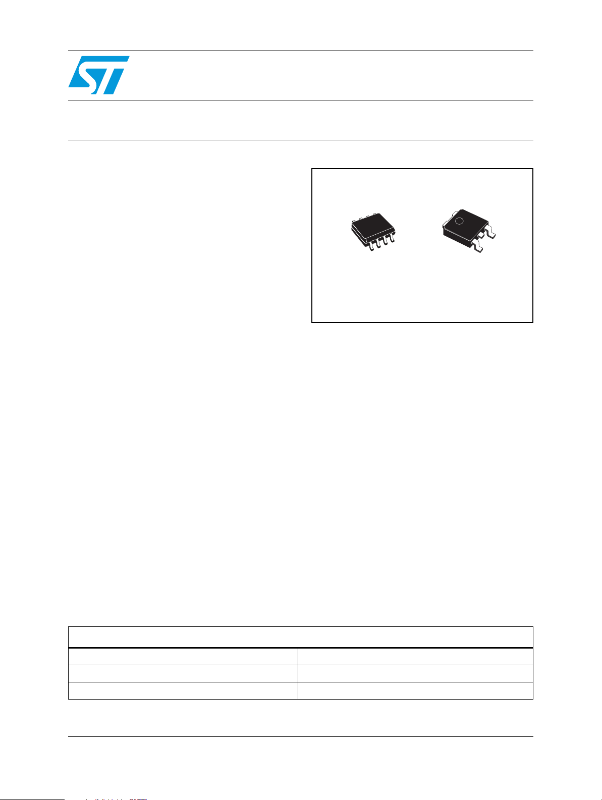
KFxxB
SO-8
DPAK
The KFxx series are very low drop regulators
available in SO-8 package and in a wide range of
output voltages.
The very low drop voltage (0.4 V) and the very low
quiescent current make them particularly
suitable for low noise, low power applications and
specially in battery powered systems.
A shutdown logic control function is available (pin
5, TTL compatible). This means that when the
device is used as a local regulator, it is possible to
put a part of the board in standby, decreasing the
total power consumption. It requires only a 2.2 µF
capacitor for stability allowing space and cost
saving.
Table 1. Device summary
Part numbers
KF15B KF40B
KF25B KF50B
KF33B KF80B
February 2008 Rev 11 1/20
www.st.com
20
Page 2

Contents KFxxB
Contents
1 Diagram . . . . . . . . . . . . . . . . . . . . . . . . . . . . . . . . . . . . . . . . . . . . . . . . . . . 3
2 Pin configuration . . . . . . . . . . . . . . . . . . . . . . . . . . . . . . . . . . . . . . . . . . . 4
3 Maximum ratings . . . . . . . . . . . . . . . . . . . . . . . . . . . . . . . . . . . . . . . . . . . . 5
4 Electrical characteristics . . . . . . . . . . . . . . . . . . . . . . . . . . . . . . . . . . . . . 6
5 Typical performance characteristics . . . . . . . . . . . . . . . . . . . . . . . . . . . 12
6 Package mechanical data . . . . . . . . . . . . . . . . . . . . . . . . . . . . . . . . . . . . 13
7 Order codes . . . . . . . . . . . . . . . . . . . . . . . . . . . . . . . . . . . . . . . . . . . . . . 18
8 Revision history . . . . . . . . . . . . . . . . . . . . . . . . . . . . . . . . . . . . . . . . . . . 19
2/20
Page 3
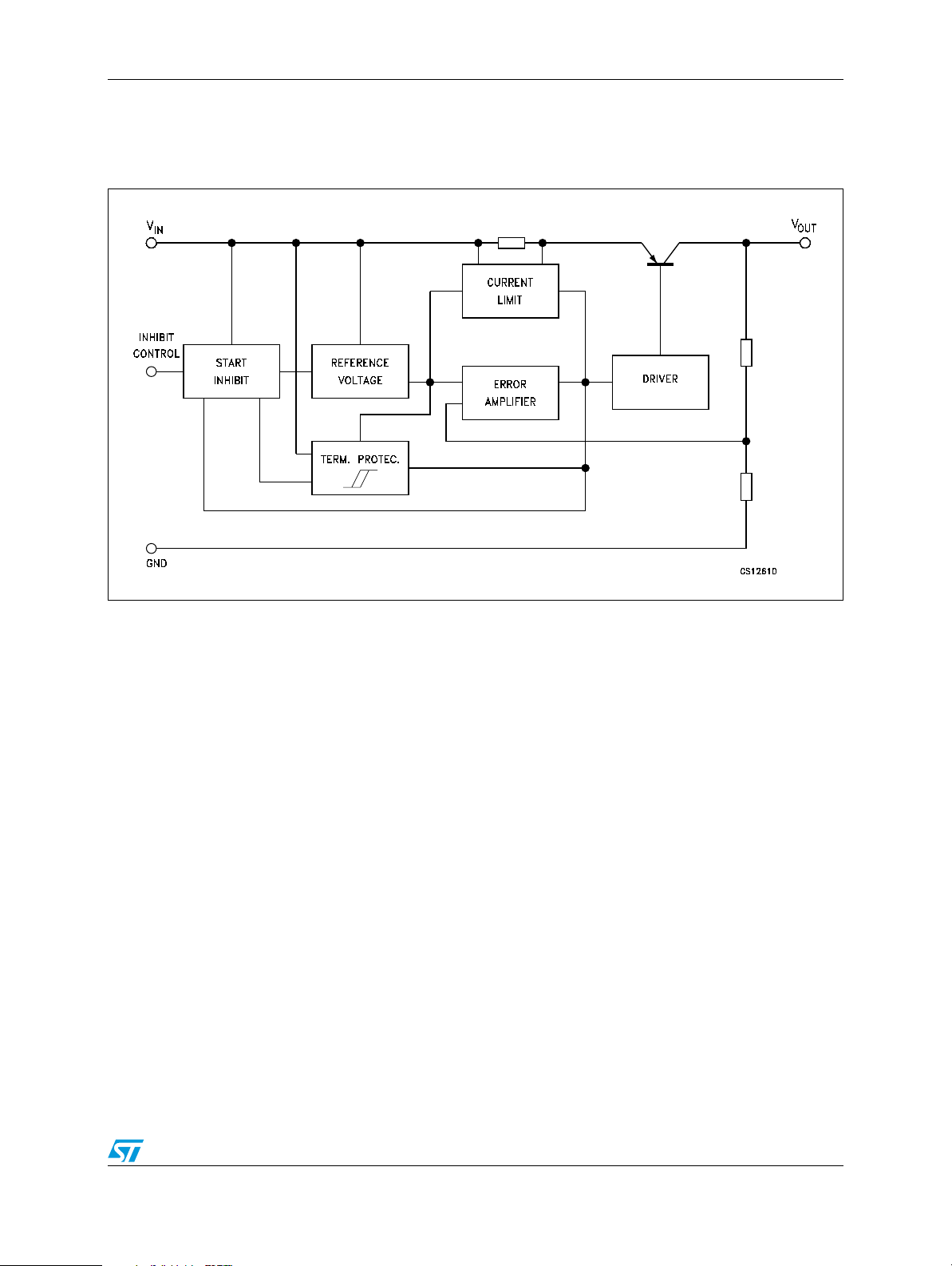
KFxxB Diagram
1 Diagram
Figure 1. Schematic diagram
3/20
Page 4
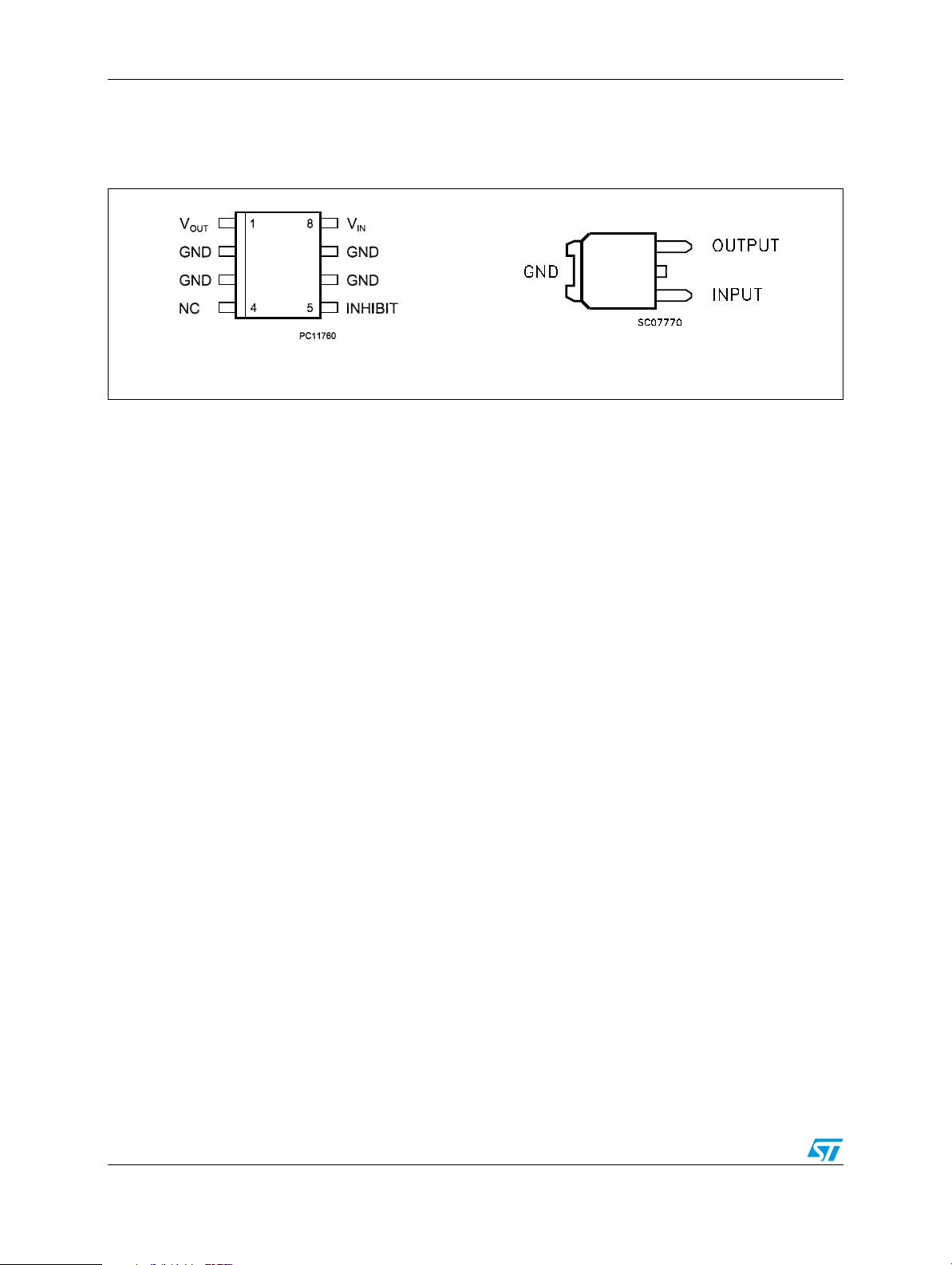
Pin configuration KFxxB
2 Pin configuration
Figure 2. Pin connections (top view)
SO-8
DPAK
4/20
Page 5
KFxxB Maximum ratings
3 Maximum ratings
Table 2. Absolute maximum ratings
Symbol Parameter Value Unit
P
T
T
V
I
I
O
TOT
STG
OP
DC input voltage -0.5 to 20 V
Output current Internally Limited
Power dissipation Internally Limited
Storage temperature range -40 to 150 °C
Operating junction temperature range -40 to 125 °C
Note: Absolute maximum ratings are those values beyond which damage to the device may occur.
Functional operation under these condition is not implied.
Table 3. Thermal data
Symbol Parameter DPAK SO-8 Unit
R
thJC
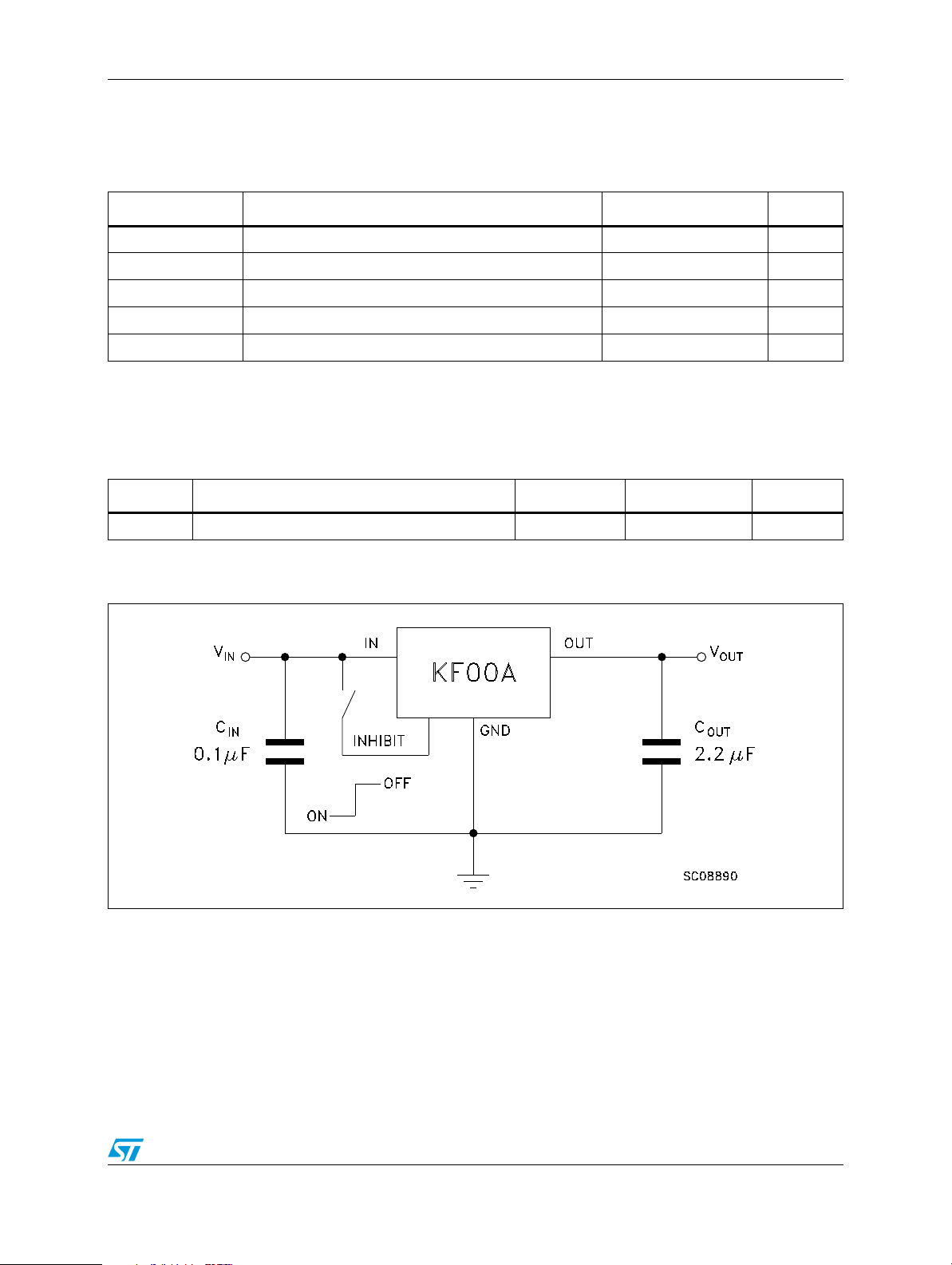
Figure 3. Test circuit
Thermal resistance junction-case 8 20 °C/W
5/20
Page 6
Electrical characteristics KFxxB
4 Electrical characteristics
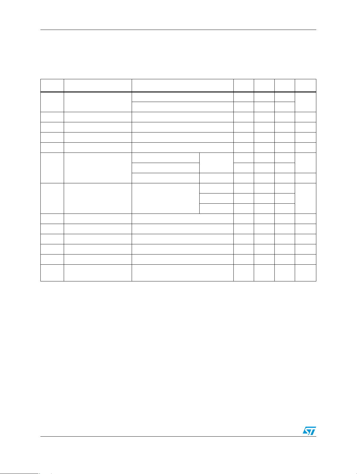
Table 4. Electrical characteristics for KF15 (refer to the test circuits, TJ = 25 °C, CI = 0.1 µF,
C
= 2.2 µF unless otherwise specified.)
O
Symbol Parameter Test conditions Min. Typ. Max. Unit
I
= 50 mA, VI = 3.5 V 1.47 1.5 1.53
V
Output voltage
O
V
Operating input voltage IO = 500 mA 2.5 20 V
I
Output current limit 1 A
I
O
ΔV
ΔV
Line regulation VI = 2.5 to 20 V, IO = 5 mA 2 12 mV
O
Load regulation VI = 2.8 V, IO = 5 to 500 mA 2 50 mV
O
I
Quiescent current
d
SVR Supply voltage rejection I
eN Output noise voltage B = 10 Hz to 100 kHz 50 µV
Dropout voltage IO = 200 mA 1 V
V
d
V
Control input logic low Ta = -40 to 125°C 0.8 V
IL
Control input logic high Ta = -40 to 125°C 2 V
V
IH
Control input current VI = 6 V, VC = 6 V 10 µA
I
I
Output bypass
C
O
capacitance
O
= 50 mA, VI = 3.5 V, Ta = -25 to 85°C 1.44 1.56
I
O
V
= 2.5 to 20V, IO = 0mA
I
= 2.8 to 20V, IO=500mA 12
V
I
V
= 6 V OFF MODE 50 100 µA
I
ON MODE
0.5 1
f = 120 Hz 82
= 5 mA, VI = 3.5 ± 1 V
O
f = 10 kHz 60
ESR = 0.1 to 10 Ω, I
= 0 to 500 mA 2 10 µF
O
V
mA
dBf = 1 kHz 77
6/20
Page 7

KFxxB Electrical characteristics
Table 5. Electrical characteristics for KF25 (refer to the test circuits, TJ = 25 °C, CI = 0.1 µF,
C
= 2.2 µF unless otherwise specified.)
O
Symbol Parameter Test conditions Min. Typ. Max. Unit
I
= 50 mA, VI = 4.5 V 2.45 2.5 2.55
V
Output voltage
O
V
Operating input voltage IO = 500 mA 20 V
I
Output current limit 1 A
I
O
ΔV
ΔV
Line regulation VI = 3.5 to 20 V, IO = 5 mA 2 12 mV
O
Load regulation VI = 3.8 V, IO = 5 to 500 mA 2 50 mV
O
I
Quiescent current
d
SVR Supply voltage rejection I
eN Output noise voltage B = 10 Hz to 100 KHz 50 µV
V
Dropout voltage
d
Control input logic low Ta = -40 to 125°C 0.8 V
V
IL
Control input logic high Ta = -40 to 125°C 2 V
V
IH
I
Control input current VI = 6 V, VC = 6 V 10 µA
I
Output bypass
C
O
capacitance
O
= 50 mA, VI = 4.5 V, Ta = -25 to 85°C 2.4 2.6
I
O
V
= 3.5 to 20V, IO = 0mA
I
= 3.8 to 20V, IO=500mA 12
V
I
V
= 6 V OFF MODE 50 100 µA
I
ON MODE
0.5 1
f = 120 Hz 82
= 5 mA, VI = 4.5 ± 1 V
O
f = 10 kHz 60
I
= 200 mA 0.2 0.35
O
= 500 mA 0.4 0.7
I
O
ESR = 0.1 to 10 Ω, I
= 0 to 500 mA 2 10 µF
O
V
mA
dBf = 1 kHz 77
V
7/20
Page 8

Electrical characteristics KFxxB
Table 6. Electrical characteristics for KF33 (refer to the test circuits, TJ = 25 °C, CI = 0.1 µF,
C
= 2.2 µF unless otherwise specified.)
O
Symbol Parameter Test conditions Min. Typ. Max. Unit
I
= 50 mA, VI = 5.3 V 3.234 3.3 3.366
V
Output voltage
O
V
Operating input voltage IO = 500 mA 20 V
I
Output current limit 1 A
I
O
ΔV
ΔV
Line regulation VI = 4.3 to 20 V, IO = 5 mA 2 12 mV
O
Load regulation VI = 4.6 V, IO = 5 to 500 mA 2 50 mV
O
I
Quiescent current
d
SVR Supply voltage rejection I
eN Output noise voltage B = 10 Hz to 100 KHz 50 µV
V
Dropout voltage
d
Control input logic low Ta = -40 to 125°C 0.8 V
V
IL
Control input logic high Ta = -40 to 125°C 2 V
V
IH
I
Control input current VI = 6 V, VC = 6 V 10 µA
I
Output bypass
C
O
capacitance
O
= 50 mA, VI = 5.3 V, Ta = -25 to 85°C 3.168 3.432
I
O
V
= 4.3 to 20V, IO = 0mA
I
= 4.6 to 20V, IO=500mA 12
V
I
V
= 6 V OFF MODE 50 100 µA
I
ON MODE
0.5 1
f = 120 Hz 80
= 5 mA, VI = 5.3 ± 1 V
O
f = 10 kHz 60
I
= 200 mA 0.2 0.35
O
= 500 mA 0.4 0.7
I
O
ESR = 0.1 to 10 Ω, I
= 0 to 500 mA 2 10 µF
O
V
mA
dBf = 1 kHz 75
V
8/20
Page 9

KFxxB Electrical characteristics
Table 7. Electrical characteristics for KF40 (refer to the test circuits, TJ = 25 °C, CI = 0.1 µF,
C
= 2.2 µF unless otherwise specified.)
O
Symbol Parameter Test conditions Min. Typ. Max. Unit
I
= 50 mA, VI = 6 V 3.9244.08
V
Output voltage
O
V
Operating input voltage IO = 500 mA 20 V
I
Output current limit 1 A
I
O
ΔV
ΔV
Line regulation VI = 5 to 20 V, IO = 5 mA 3 18 mV
O
Load regulation VI = 5.3 V, IO = 5 to 500 mA 2 50 mV
O
I
Quiescent current
d
SVR Supply voltage rejection I
eN Output noise voltage B = 10 Hz to 100 KHz 50 µV
V
Dropout voltage
d
Control input logic low Ta = -40 to 125°C 0.8 V
V
IL
Control input logic high Ta = -40 to 125°C 2 V
V
IH
I
Control input current VI = 6 V, VC = 6 V 10 µA
I
Output bypass
C
O
capacitance
O
= 50 mA, VI = 6 V, Ta = -25 to 85°C 3.84 4.16
I
O
V
= 5 to 20V, IO = 0mA
I
= 5.3 to 20V, IO=500mA 12
V
I
V
= 6 V OFF MODE 50 100 µA
I
ON MODE
0.5 1
f = 120 Hz 78
= 5 mA, VI = 6 ± 1 V
O
f = 10 kHz 60
I
= 200 mA 0.2 0.35
O
= 500 mA 0.4 0.7
I
O
ESR = 0.1 to 10 Ω, I
= 0 to 500 mA 2 10 µF
O
V
mA
dBf = 1 kHz 73
V
9/20
Page 10

Electrical characteristics KFxxB
Table 8. Electrical characteristics for KF50 (refer to the test circuits, TJ = 25 °C, CI = 0.1 µF,
C
= 2.2 µF unless otherwise specified.)
O
Symbol Parameter Test conditions Min. Typ. Max. Unit
I
= 50 mA, VI = 7 V 4.9 5 5.1
V
Output voltage
O
V
Operating input voltage IO = 500 mA 20 V
I
Output current limit 1 A
I
O
ΔV
ΔV
Line regulation VI = 6 to 20 V, IO = 5 mA 3 18 mV
O
Load regulation VI = 6.3 V, IO = 5 to 500 mA 2 50 mV
O
I
Quiescent current
d
SVR Supply voltage rejection I
eN Output noise voltage B = 10 Hz to 100 KHz 50 µV
V
Dropout voltage
d
Control input logic low Ta = -40 to 125°C 0.8 V
V
IL
Control input logic high Ta = -40 to 125°C 2 V
V
IH
I
Control input current VI = 6 V, VC = 6 V 10 µA
I
Output bypass
C
O
capacitance
O
= 50 mA, VI = 7 V, Ta = -25 to 85°C 4.8 5.2
I
O
V
= 6 to 20V, IO = 0mA
I
= 6.3 to 20V, IO=500mA 12
V
I
V
= 6 V OFF MODE 50 100 µA
I
ON MODE
0.5 1
f = 120 Hz 76
= 5 mA, VI = 7 ± 1 V
O
f = 10 kHz 60
I
= 200 mA 0.2 0.35
O
= 500 mA 0.4 0.7
I
O
ESR = 0.1 to 10 Ω, I
= 0 to 500 mA 2 10 µF
O
V
mA
dBf = 1 kHz 71
V
10/20
Page 11

KFxxB Electrical characteristics
Table 9. Electrical characteristics for KF80 (refer to the test circuits, TJ = 25 °C, CI = 0.1 µF,
C
= 2.2 µF unless otherwise specified.)
O
Symbol Parameter Test conditions Min. Typ. Max. Unit
I
= 50 mA, VI = 10 V 7.84 8 8.16
V
Output voltage
O
V
Operating input voltage IO = 500 mA 20 V
I
Output current limit 1 A
I
O
ΔV
ΔV
Line regulation VI = 9 to 20 V, IO = 5 mA 4 24 mV
O
Load regulation VI = 9.3 V, IO = 5 to 500 mA 2 50 mV
O
I
Quiescent current
d
SVR Supply voltage rejection I
eN Output noise voltage B = 10 Hz to 100 KHz 50 µV
V
Dropout voltage
d
Control input logic low Ta = -40 to 125°C 0.8 V
V
IL
Control input logic high Ta = -40 to 125°C 2 V
V
IH
I
Control input current VI = 6 V, VC = 6 V 10 µA
I
Output bypass
C
O
capacitance
O
= 50 mA, VI = 10 V, Ta = -25 to 85°C 7.68 8.32
I
O
V
= 9 to 20V, IO = 0mA
I
= 9.3 to 20V, IO=500mA 12
V
I
V
= 9 V OFF MODE 70 140 µA
I
ON MODE
0.7 1.5
f = 120 Hz 72
= 5 mA, VI = 10 ± 1 V
O
f = 10 kHz 60
I
= 200 mA 0.2 0.35
O
= 500 mA 0.4 0.7
I
O
ESR = 0.1 to 10 Ω, I
= 0 to 500 mA 2 10 µF
O
V
mA
dBf = 1 kHz 67
V
11/20
Page 12

Typical performance characteristics KFxxB
5 Typical performance characteristics
(unless otherwise specified V
Figure 4. Dropout voltage vs output current Figure 5. Dropout voltage vs temperature
Figure 6. Supply current vs input voltage Figure 7. Supply current vs input voltage
O(NOM)
= 3.3 V)
Figure 8. Short circuit current vs input
12/20
voltage
Figure 9. Supply current vs temperature
Page 13

KFxxB Package mechanical data
6 Package mechanical data
In order to meet environmental requirements, ST offers these devices in ECOPACK®
packages. These packages have a lead-free second level interconnect. The category of
second Level Interconnect is marked on the package and on the inner box label, in
compliance with JEDEC Standard JESD97. The maximum ratings related to soldering
conditions are also marked on the inner box label. ECOPACK is an ST trademark.
ECOPACK specifications are available at: www.st.com.
13/20
Page 14

Package mechanical data KFxxB
SO-8 mechanical data
Dim.
Min. Typ. Max. Min. Typ. Max.
mm. inch.
A1.35 1.75 0.053 0.069
A1 0.10 0.25 0.04 0.010
A2 1.10 1.65 0.043 0.065
B0.33 0.51 0.013 0.020
C0.19 0.25 0.007 0.010
D4.80 5.00 0.189 0.197
E 3.80 4.00 0.150 0.157
e 1.27 0.050
H5.80 6.20 0.228 0.244
h 0.25 0.50 0.010 0.020
L 0.40 1.27 0.016 0.050
k 8° (max.)
ddd 0.1 0.04
14/20
0016023/C
Page 15

KFxxB Package mechanical data
DPAK mechanical data
Dim.
Min. Typ. Max. Min. Typ. Max.
A 2.2 2.4 0.086 0.094
A1 0.9 1.1 0.035 0.043
A2 0.03 0.23 0.001 0.009
B 0.64 0.9 0.025 0.035
b4 5.2 5.4 0.204 0.212
C 0.45 0.6 0.017 0.023
C2 0.48 0.6 0.019 0.023
D 6 6.2 0.236 0.244
D1 5.1 0.200
E 6.4 6.6 0.252 0.260
E1 4.7 0.185
e2.28 0.090
e1 4.4 4.6 0.173 0.181
H 9.35 10.1 0.368 0.397
L 1 0.039
(L1)
L2 0.8 0.031
L4 0.6 1 0.023 0.039
R 0.2 0.008
V2 0° 8°0° 8°
mm. inch.
2.8 0.110
0068772-F
15/20
Page 16

Package mechanical data KFxxB
Tape & reel SO-8 mechanical data
mm. inch.
Dim.
Min. Typ. Max. Min. Typ. Max.
A 330 12.992
C 12.8 13.2 0.504 0.519
D 20.2 0.795
N60 2.362
T 22.4 0.882
Ao 8.1 8.5 0.319 0.335
Bo 5.5 5.9 0.216 0.232
Ko 2.1 2.3 0.082 0.090
Po 3.9 4.1 0.153 0.161
P7.98.1 0.311 0.319
16/20
Page 17

KFxxB Package mechanical data
Tape & reel DPAK-PPAK mechanical data
Dim.
Min. Typ. Max. Min. Typ. Max.
A 330 12.992
C12.8 13.0 13.2 0.504 0.512 0.519
D 20.2 0.795
N60 2.362
T22.40.882
Ao 6.806.90 7.00 0.268 0.272 0.2.76
Bo 10.40 10.50 10.60 0.409 0.413 0.417
Ko 2.55 2.65 2.75 0.100 0.104 0.105
Po 3.9 4.0 4.1 0.153 0.157 0.161
P7.98.0 8.1 0.311 0.315 0.319
mm. inch.
17/20
Page 18

Order codes KFxxB
7 Order codes
Table 10. Order codes
Packages
Output voltage
SO-8 (tape and reel) DPAK (tape and reel)
KF15BDT-TR 1.5 V
KF25BD-TR KF25BDT-TR 2.5 V
KF33BD-TR KF33BDT-TR 3.3 V
KF40BDT-TR 4 V
KF50BD-TR KF50BDT-TR 5 V
KF80BDT-TR 8 V
18/20
Page 19

KFxxB Revision history
8 Revision history
Table 11. Document revision history
Date Revision Changes
06-Jun-2007 9 Order codes updated.
14-Dec-2007 10 Modified: Ta bl e 1 0.
21-Feb-2008 11 Modified: Table 10 on page 18.
19/20
Page 20

KFxxB
Please Read Carefully:
Information in this document is provided solely in connection with ST products. STMicroelectronics NV and its subsidiaries (“ST”) reserve the
right to make changes, corrections, modifications or improvements, to this document, and the products and services described herein at any
time, without notice.
All ST products are sold pursuant to ST’s terms and conditions of sale.
Purchasers are solely responsible for the choice, selection and use of the ST products and services described herein, and ST assumes no
liability whatsoever relating to the choice, selection or use of the ST products and services described herein.
No license, express or implied, by estoppel or otherwise, to any intellectual property rights is granted under this document. If any part of this
document refers to any third party products or services it shall not be deemed a license grant by ST for the use of such third party products
or services, or any intellectual property contained therein or considered as a warranty covering the use in any manner whatsoever of such
third party products or services or any intellectual property contained therein.
UNLESS OTHERWISE SET FORTH IN ST’S TERMS AND CONDITIONS OF SALE ST DISCLAIMS ANY EXPRESS OR IMPLIED
WARRANTY WITH RESPECT TO THE USE AND/OR SALE OF ST PRODUCTS INCLUDING WITHOUT LIMITATION IMPLIED
WARRANTIES OF MERCHANTABILITY, FITNESS FOR A PARTICULAR PURPOSE (AND THEIR EQUIVALENTS UNDER THE LAWS
OF ANY JURISDICTION), OR INFRINGEMENT OF ANY PATENT, COPYRIGHT OR OTHER INTELLECTUAL PROPERTY RIGHT.
UNLESS EXPRESSLY APPROVED IN WRITING BY AN AUTHORIZE REPRESENTATIVE OF ST, ST PRODUCTS ARE NOT DESIGNED,
AUTHORIZED OR WARRANTED FOR USE IN MILITARY, AIR CRAFT, SPACE, LIFE SAVING, OR LIFE SUSTAINING APPLICATIONS,
NOR IN PRODUCTS OR SYSTEMS, WHERE FAILURE OR MALFUNCTION MAY RESULT IN PERSONAL INJURY, DEATH, OR
SEVERE PROPERTY OR ENVIRONMENTAL DAMAGE.
Resale of ST products with provisions different from the statements and/or technical features set forth in this document shall immediately void
any warranty granted by ST for the ST product or service described herein and shall not create or extend in any manner whatsoever, any
liability of ST.
ST and the ST logo are trademarks or registered trademarks of ST in various countries.
Information in this document supersedes and replaces all information previously supplied.
The ST logo is a registered trademark of STMicroelectronics. All other names are the property of their respective owners.
© 2008 STMicroelectronics - All rights reserved
STMicroelectronics group of companies
Australia - Belgium - Brazil - Canada - China - Czech Republic - Finland - France - Germany - Hong Kong - India - Israel - Italy - Japan -
Malaysia - Malta - Morocco - Singapore - Spain - Sweden - Switzerland - United Kingdom - United States of America
www.st.com
20/20
 Loading...