

5 A low drop positive voltage regulator adjustable and fixed
Features
■ Typical dropout 1.3 V (at 5 A)
■ Three terminal adjustable or fixed output
voltage 1.8 V, 3.3 V.
■ Guaranteed output current up to 5 A
■ Output tolerance ± 1% at 25 °C and ± 2% in full
temperature range for the "A" version
■ Output tolerance ± 2% at 25 °C and ± 3% in full
temperature range internal power and thermal
limit
■ Wide operating temp. range -40 °C to 125 °C
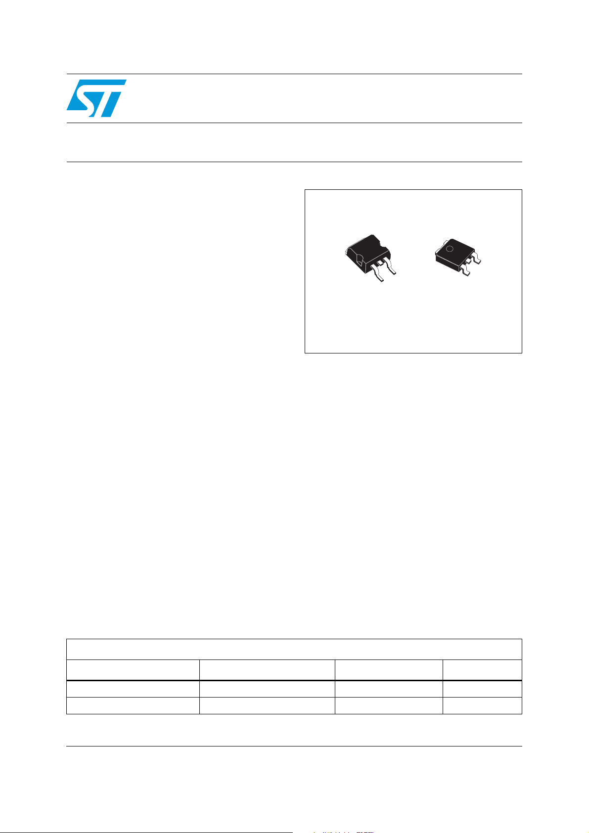
■ Package available: D²PAK and DPAK
■ Pinout compatibility with standard adjustable
VREG
KD1084AXX
KD1084AXX18
D²PAK
"A" version and ± 2% at 25 °C for standard
version.
DPAK
Description
The KD1084 is a low drop voltage regulator able
to provide up to 5 A of output current. Dropout is
guaranteed at a maximum of 1.5 V at the
maximum output current, decreasing at lower
loads. The KD1084 is pin to pin compatible with
he older 3-terminal adjustable regulators but has
better performances in term of drop and output
tolerance. A 2.85 V output version is suitable for
SCSI-2 active termination. Unlike PNP regulators,
where a part of the output current is wasted as
quiescent current, the KD1084 quiescent current
flows into the load, so increase efficiency. Only a
10 µF minimum capacitor is need for stability. The
devices are supplied in D²PAK and DPAK. On chip
trimming allows the regulator to reach a very tight
output voltage tolerance, within ±1% at 25 °C for
Table 1. Device summary
D²PA K DPAK Out p ut vo l t age Tol e ran c e
KD1084AD2T18R 1.8 V 1%
Order codes
KD1084ADT-R ADJ 1%
May 2011 Doc ID 8761 Rev 11 1/17
www.st.com
17

Contents KD1084AXX, KD1084AXX18
Contents
1 Diagram . . . . . . . . . . . . . . . . . . . . . . . . . . . . . . . . . . . . . . . . . . . . . . . . . . . 3
2 Pin configuration . . . . . . . . . . . . . . . . . . . . . . . . . . . . . . . . . . . . . . . . . . . 4
3 Maximum ratings . . . . . . . . . . . . . . . . . . . . . . . . . . . . . . . . . . . . . . . . . . . . 5
4 Schematic application . . . . . . . . . . . . . . . . . . . . . . . . . . . . . . . . . . . . . . . 6
5 Electrical characteristics . . . . . . . . . . . . . . . . . . . . . . . . . . . . . . . . . . . . . 7
6 Typical application . . . . . . . . . . . . . . . . . . . . . . . . . . . . . . . . . . . . . . . . . . 9
7 Package mechanical data . . . . . . . . . . . . . . . . . . . . . . . . . . . . . . . . . . . . 11
8 Revision history . . . . . . . . . . . . . . . . . . . . . . . . . . . . . . . . . . . . . . . . . . . 16
2/17 Doc ID 8761 Rev 11
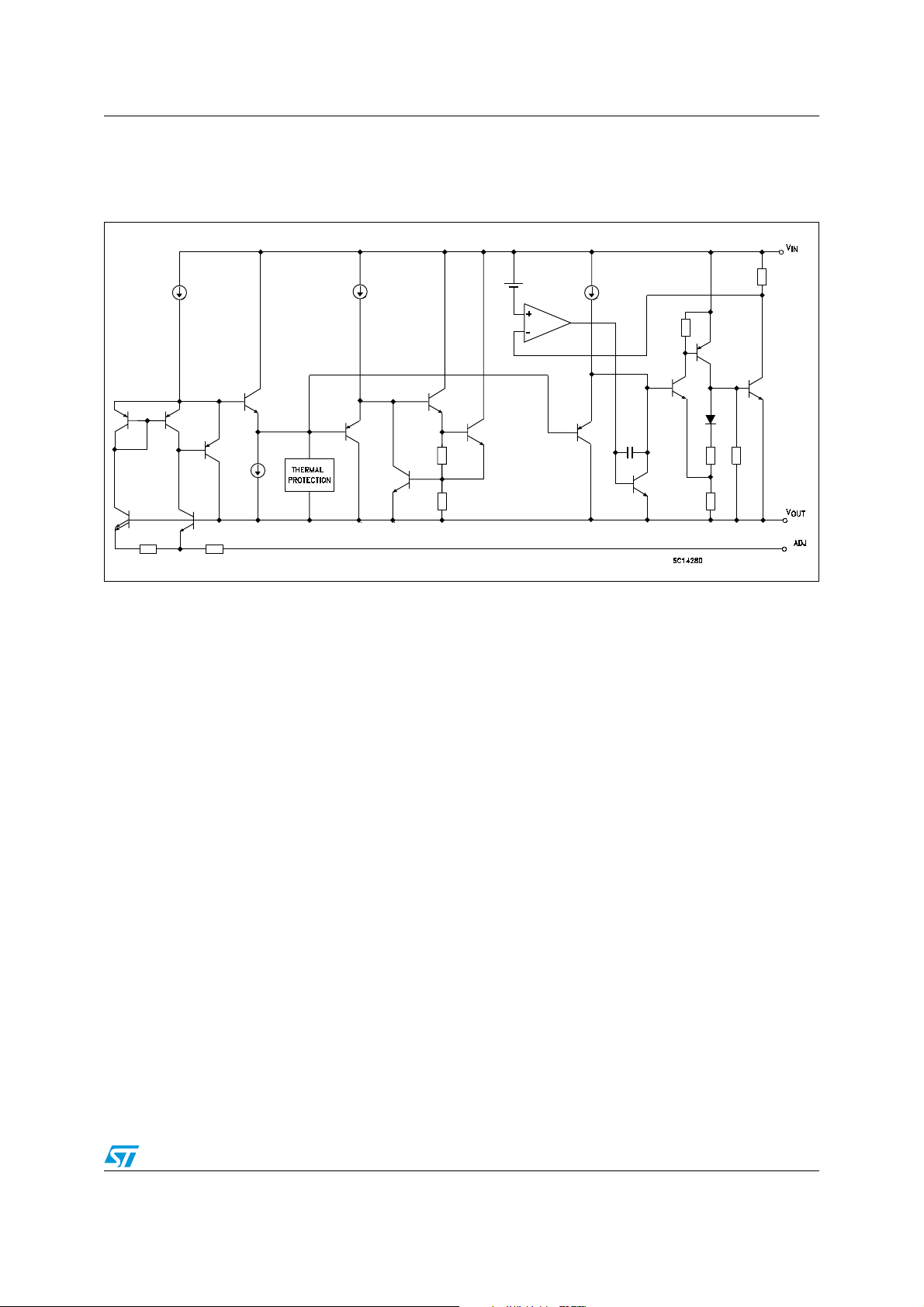
KD1084AXX, KD1084AXX18 Diagram
1 Diagram
Figure 1. Schematic diagram
Doc ID 8761 Rev 11 3/17
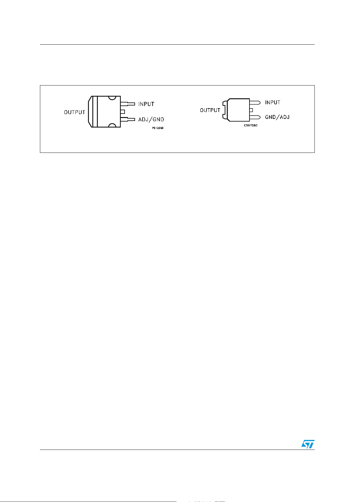
Pin configuration KD1084AXX, KD1084AXX18
2 Pin configuration
Figure 2. Pin connections (top view)
D²PAK
DPAK
4/17 Doc ID 8761 Rev 11
KD1084AXX, KD1084AXX18 Maximum ratings
3 Maximum ratings
Table 2. Absolute maximum ratings
Symbol Parameter Value Unit
T
P
T
V
I
I
O
D
STG
OP
DC input voltage 12 V
Output current Internally limited
Power dissipation Internally limited
Storage temperature range -55 to +150 °C
Operating junction temperature range -40 to +125 °C
Note: Absolute maximum ratings are those values beyond which damage to the device may occur.
Functional operation under these condition is not implied.
Table 3. Thermal data
Symbol Parameter DPAK D²PAK Unit
R
R
thJC
thJA
Thermal resistance junction-case 8 3 °C/W
Thermal resistance junction-ambient 100 62.5 °C/W
Doc ID 8761 Rev 11 5/17
Schematic application KD1084AXX, KD1084AXX18
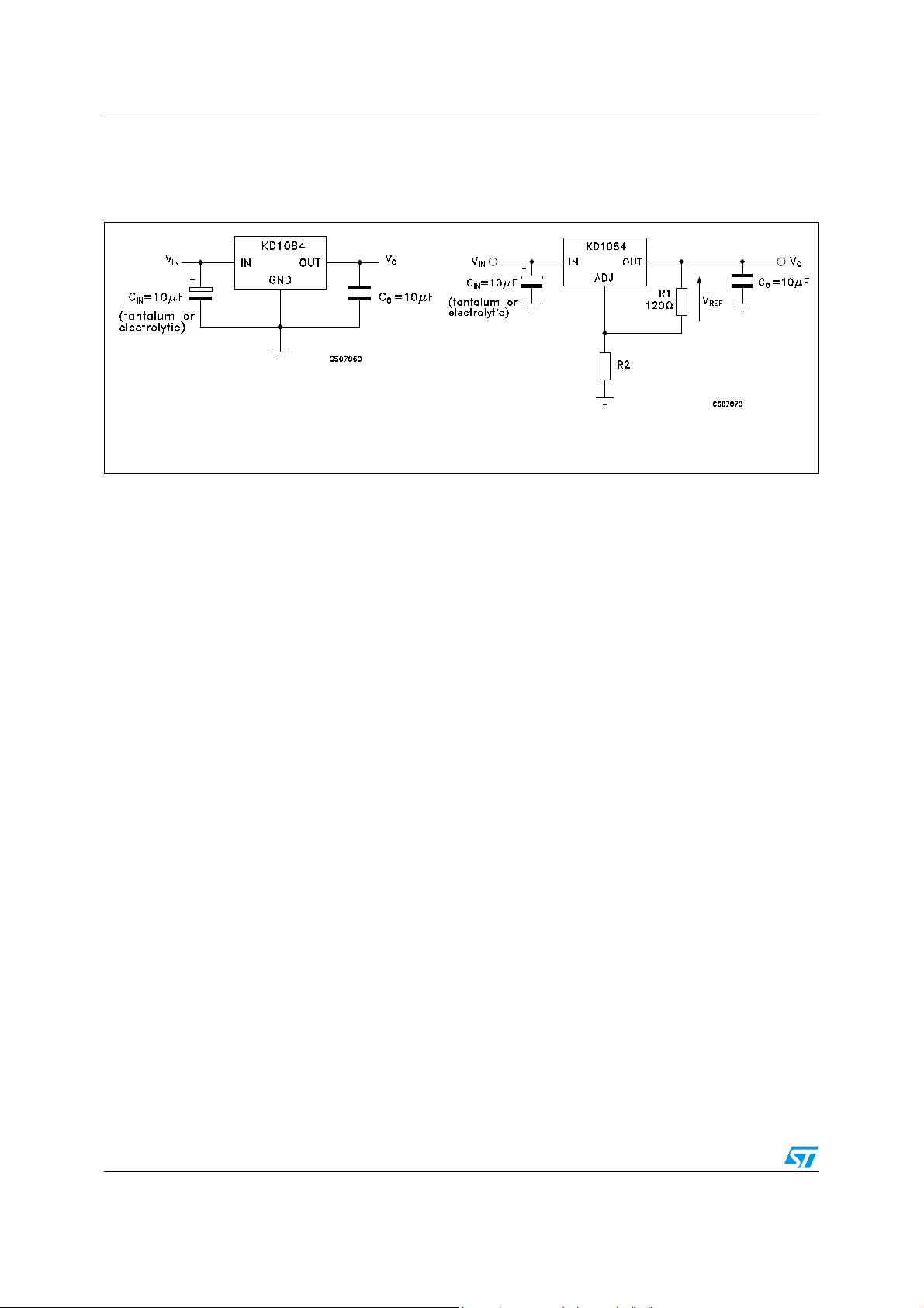
4 Schematic application
Figure 3. Application circuit
R
2
V
REF
⎛⎞
1
------ -+
⋅=
⎝⎠
R
1
V
O
6/17 Doc ID 8761 Rev 11

KD1084AXX, KD1084AXX18 Electrical characteristics
5 Electrical characteristics
VI = 4.8 V, CI = CO = 10 µF (tant.), TA = -40 to 125 °C, unless otherwise specified.
Table 4. Electrical characteristics of KD1084AXX18
Symbol Parameter Test conditions Min. Typ. Max. Unit
V
O
ΔV
O
ΔV
O
V
d
I
q
I
sc
SVR Supply voltage rejection
eN
S Temperature stability 0.5 %
S Long term stability T
I
= 0 mA, TJ = 25 °C 1.782 1.8 1.818 V
Output voltage
O
= 0 to 5 A, VI = 3.4 to 10 V 1.764 1.8 1.836 V
I
O
IO = 0 mA, VI = 3.4 to 10 V TJ = 25 °C 0.5 6 mV
Line regulation
= 0 mA, VI = 3.4 to 10 V 1 6 mV
I
O
I
= 0 to 5 A, TJ = 25 °C 3 15 mV
Load regulation
O
I
= 0 to 5 A 7 20 mV
O
Dropout voltage IO = 5 A 1.3 1.5 V
Quiescent current VI ≤ 10 V 5 10 mA
Short circuit current VI - VO = 5 V 5.5 7 A
Thermal regulation T
RMS output noise voltage
(% of V
)
O
= 25 °C, 30 ms pulse 0.003 0.015 %/W
A
f = 120 Hz, C
VI = 5.3 ± 1.5 V
= 25 °C, f = 10 Hz to 10 kHz 0.003 %
T
A
= 125 °C, 1000 Hrs 0.5 %
A
= 25 µF, IO = 5 A
O
60 75 dB
Doc ID 8761 Rev 11 7/17

Electrical characteristics KD1084AXX, KD1084AXX18
VI = 4.25 V, CI = CO = 10 µF (tant.), TA = -40 to 125°C, unless otherwise specified.
Table 5. Electrical characteristics of KD1084AXX
Symbol Parameter Test conditions Min. Typ. Max. Unit
V
O
ΔV
O
ΔV
O
V
d
I
O(min)
I
sc
SVR Supply voltage rejection
I
= 10 mA, TJ = 25 °C 1.237 1.25 1.263 V
Output voltage
Line regulation
O
I
= 10 mA to 5 A, VI = 2.85 to 10 V 1.225 1.25 1.275 V
O
I
= 10 mA, VI = 2.85 to 10 V TJ = 25 °C 0.015 0.2
O
I
= 10 mA, VI = 2.85 to 10 V 0.035 0.2
O
%
IO = 10 mA to 5 A, TJ = 25 °C 0.1 0.3
Load regulation
= 10 mA to 5 A 0.2 0.4
I
O
Dropout voltage IO = 5 A 1.3 1.5 V
Quiescent current VI ≤ 10 V 3 10 mA
Short circuit current VI - VO = 5 V 5.5 7 A
Thermal regulation T
= 25 °C, 30 ms pulse 0.003 0.015 %/W
A
f = 120 Hz, C
= 25 µF, C
O
IO = 5 A, VI = 4.75 ± 1.5 V
ADJ
= 25 µF,
60 72 dB
I
ΔI
Adjust pin current VI = 4.25V, IO = 10 mA 55 120 µA
ADJ
Adjust pin current change VI = 2.85 to 10 V, IO = 10 mA to 5 A 0.2 5 µA
ADJ
RMS Output noise voltage
eN
(% of V
)
O
= 25 °C, f = 10 Hz to 10 kHz 0.003 %
T
A
S Temperature stability 0.5 %
S Long term stability T
= 125 °C, 1000 Hrs 0.5 %
A
8/17 Doc ID 8761 Rev 11

KD1084AXX, KD1084AXX18 Typical application
6 Typical application
Unless otherwise specified TJ = 25 °C, CI = CO = 10 µF (tant.)
Figure 4. Dropout voltage vs. output current Figure 5. Dropout voltage vs. temperature
Figure 6. Short circuit current vs. dropout
Figure 8. Output voltage vs. temperature Figure 9. Load regulation vs. temperature
voltage
Figure 7. Line regulation vs. temperature
Doc ID 8761 Rev 11 9/17

Typical application KD1084AXX, KD1084AXX18
Figure 10. Supply voltage rejection vs.
Figure 12. Line transient Figure 13. Load transient
frequency
Figure 11. Adjust pin current vs. output
current
VI = 4 to 6 V, IO = 200 mA, CI = 1 µF (tant), CO = 10 µF
(tant), ts = tf = 5 µs
10/17 Doc ID 8761 Rev 11
VI = 7 V, IO = 0.1 to 5 A, CI = 1 µF (tant), CO = 10 µF (tant),
ts = tf = 3.5 µs

KD1084AXX, KD1084AXX18 Package mechanical data
7 Package mechanical data
In order to meet environmental requirements, ST offers these devices in different grades of
ECOPACK
specifications, grade definitions and product status are available at: www.st.com.
ECOPACK
®
packages, depending on their level of environmental compliance. ECOPACK®
®
is an ST trademark.
Doc ID 8761 Rev 11 11/17

Package mechanical data KD1084AXX, KD1084AXX18
DPAK mechanical data
Dim.
mm. inch.
Min. Typ. Max. Min. Typ. Max.
A 2.2 2.4 0.086 0.094
A1 0.9 1.1 0.035 0.043
A2 0.03 0.23 0.001 0.009
b 0.64 0.9 0.025 0.035
b4 5.2 5.4 0.204 0.212
C 0.45 0.6 0.017 0.023
C2 0.48 0.6 0.019 0.023
D 6 6.2 0.236 0.244
D1 5.1 0.200
E 6.4 6.6 0.252 0.260
E1 4.7 0.185
e2.28 0.090
e1 4.4 4.6 0.173 0.181
H 9.35 10.1 0.368 0.397
L 1 0.039
(L1)
2.8 0.110
L2 0.8 0.031
L4 0.6 1 0.023 0.039
R 0.2 0.008
V2 0° 8°0° 8°
12/17 Doc ID 8761 Rev 11
0068772-F

KD1084AXX, KD1084AXX18 Package mechanical data
D²PAK mechanical data
mm. inch.
Dim.
Min. Typ. Max. Min. Typ. Max.
A 4.4 4.6 0.173 0.181
A1 2.49 2.69 0.098 0.106
A2 0.03 0.23 0.001 0.009
B 0.7 0.93 0.027 0.036
B2 1.14 1.7 0.044 0.067
C 0.45 0.6 0.017 0.023
C2 1.23 1.36 0.048 0.053
D 8.95 9.350.352 0.368
D1 8 0.315
E 10 10.4 0.393 0.409
E1 8.5 0.335
G4.88 5.28 0.192 0.208
L 15 15.85 0.590 0.624
L2 1.27 1.4 0.050 0.055
L3 1.4 1.75 0.055 0.068
M2.4 3.2 0.094 0.126
R 0.4 0.016
V2 0° 8°0° 8°
P011P6G
Doc ID 8761 Rev 11 13/17

Package mechanical data KD1084AXX, KD1084AXX18
Tape & reel DPAK-PPAK mechanical data
Dim.
mm. inch.
Min. Typ. Max. Min. Typ. Max.
A 330 12.992
C12.8 13.0 13.2 0.504 0.512 0.519
D 20.2 0.795
N60 2.362
T22.40.882
Ao 6.806.90 7.00 0.268 0.272 0.2.76
Bo 10.40 10.50 10.60 0.409 0.413 0.417
Ko 2.55 2.65 2.75 0.100 0.104 0.105
Po 3.9 4.0 4.1 0.153 0.157 0.161
P7.98.0 8.1 0.311 0.315 0.319
14/17 Doc ID 8761 Rev 11

KD1084AXX, KD1084AXX18 Package mechanical data
Tape & reel D²PAK-P²PAK-D²PAK/A-P²PAK/A mechanical data
Dim.
mm. inch.
Min. Typ. Max. Min. Typ. Max.
A180 7.086
C 12.8 13.0 13.2 0.504 0.512 0.519
D 20.2 0.795
N60 2.362
T 14.4 0.567
Ao 10.50 10.6 10.70 0.413 0.417 0.421
Bo 15.70 15.80 15.90 0.618 0.622 0.626
Ko 4.804.90 5.00 0.189 0.193 0.197
Po 3.9 4.0 4.1 0.153 0.157 0.161
P 11.9 12.0 12.1 0.468 0.472 0.476
Doc ID 8761 Rev 11 15/17

Revision history KD1084AXX, KD1084AXX18
8 Revision history
Table 6. Document revision history
Date Revision Changes
06-Sep-2005 4 Order codes updated.
02-Apr-2007 5 Order codes updated.
30-May-2007 6 Order codes updated.
18-Dec-2007 7 Added Ta b l e 1 .
21-Feb-2008 8 Modified: Table 1 on page 1.
16-Jul-2008 9 Modified: Table 1 on page 1.
28-Jul-2009 10 Modified: Table 1 on page 1.
12-May-2011 11 Modified: Table 5 on page 8.
16/17 Doc ID 8761 Rev 11

KD1084AXX, KD1084AXX18
Please Read Carefully:
Information in this document is provided solely in connection with ST products. STMicroelectronics NV and its subsidiaries (“ST”) reserve the
right to make changes, corrections, modifications or improvements, to this document, and the products and services described herein at any
time, without notice.
All ST products are sold pursuant to ST’s terms and conditions of sale.
Purchasers are solely responsible for the choice, selection and use of the ST products and services described herein, and ST assumes no
liability whatsoever relating to the choice, selection or use of the ST products and services described herein.
No license, express or implied, by estoppel or otherwise, to any intellectual property rights is granted under this document. If any part of this
document refers to any third party products or services it shall not be deemed a license grant by ST for the use of such third party products
or services, or any intellectual property contained therein or considered as a warranty covering the use in any manner whatsoever of such
third party products or services or any intellectual property contained therein.
UNLESS OTHERWISE SET FORTH IN ST’S TERMS AND CONDITIONS OF SALE ST DISCLAIMS ANY EXPRESS OR IMPLIED
WARRANTY WITH RESPECT TO THE USE AND/OR SALE OF ST PRODUCTS INCLUDING WITHOUT LIMITATION IMPLIED
WARRANTIES OF MERCHANTABILITY, FITNESS FOR A PARTICULAR PURPOSE (AND THEIR EQUIVALENTS UNDER THE LAWS
OF ANY JURISDICTION), OR INFRINGEMENT OF ANY PATENT, COPYRIGHT OR OTHER INTELLECTUAL PROPERTY RIGHT.
UNLESS EXPRESSLY APPROVED IN WRITING BY AN AUTHORIZED ST REPRESENTATIVE, ST PRODUCTS ARE NOT
RECOMMENDED, AUTHORIZED OR WARRANTED FOR USE IN MILITARY, AIR CRAFT, SPACE, LIFE SAVING, OR LIFE SUSTAINING
APPLICATIONS, NOR IN PRODUCTS OR SYSTEMS WHERE FAILURE OR MALFUNCTION MAY RESULT IN PERSONAL INJURY,
DEATH, OR SEVERE PROPERTY OR ENVIRONMENTAL DAMAGE. ST PRODUCTS WHICH ARE NOT SPECIFIED AS "AUTOMOTIVE
GRADE" MAY ONLY BE USED IN AUTOMOTIVE APPLICATIONS AT USER’S OWN RISK.
Resale of ST products with provisions different from the statements and/or technical features set forth in this document shall immediately void
any warranty granted by ST for the ST product or service described herein and shall not create or extend in any manner whatsoever, any
liability of ST.
ST and the ST logo are trademarks or registered trademarks of ST in various countries.
Information in this document supersedes and replaces all information previously supplied.
The ST logo is a registered trademark of STMicroelectronics. All other names are the property of their respective owners.
© 2011 STMicroelectronics - All rights reserved
Australia - Belgium - Brazil - Canada - China - Czech Republic - Finland - France - Germany - Hong Kong - India - Israel - Italy - Japan -
STMicroelectronics group of companies
Malaysia - Malta - Morocco - Philippines - Singapore - Spain - Sweden - Switzerland - United Kingdom - United States of America
www.st.com
Doc ID 8761 Rev 11 17/17
 Loading...