

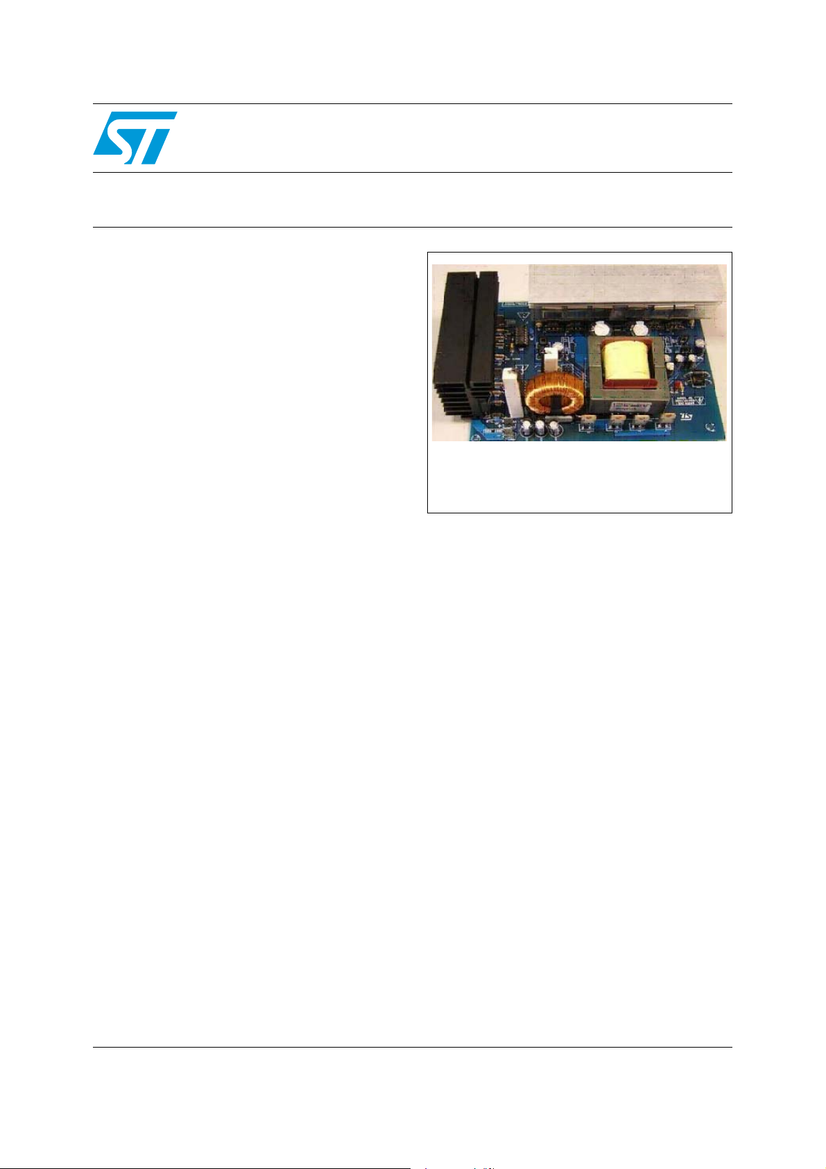
1000 W dual stage DC-AC converter demonstration board
Features
■ Nominal input voltage: 24 V
■ Output voltage: 230 Vrms, 50 Hz
■ Output power: 1 kW
■ Efficiency: 90%
■ Switching frequency: 100 kHz (DC-DC); 16
kHz (DC-AC)
Description
The STEVAL-ISV001V1 demonstration board
implements a 1 kW dual stage DC-AC converter,
suitable for use in battery powered uninterruptible
power supplies (UPS) or photovoltaic (PV) stand
alone systems. The converter is powered from a
low DC input voltage varying from 20 V to 28 V
and is capable of supplying up to 1 kW output
power on a single phase AC load. These features
are met with a dual stage conversion topology
including an efficient step-up push-pull DC-DC
converter, to produce a regulated high voltage DC
bus, and a sinusoidal h-bridge PWM inverter to
generate a 50 Hz, 230 Vrms output sine wave.
Other relevant features of the proposed system
are high power density, high switching frequency,
galvanic isolation and efficiency greater than 90%
over a wide output load range.
STEVAL-ISV001V1
based on the STP160N75F3
Data Brief
STEVAL-ISV001V1
November 2008 Rev 1 1/6
For further information contact your local STMicroelectronics sales office.
www.st.com
6
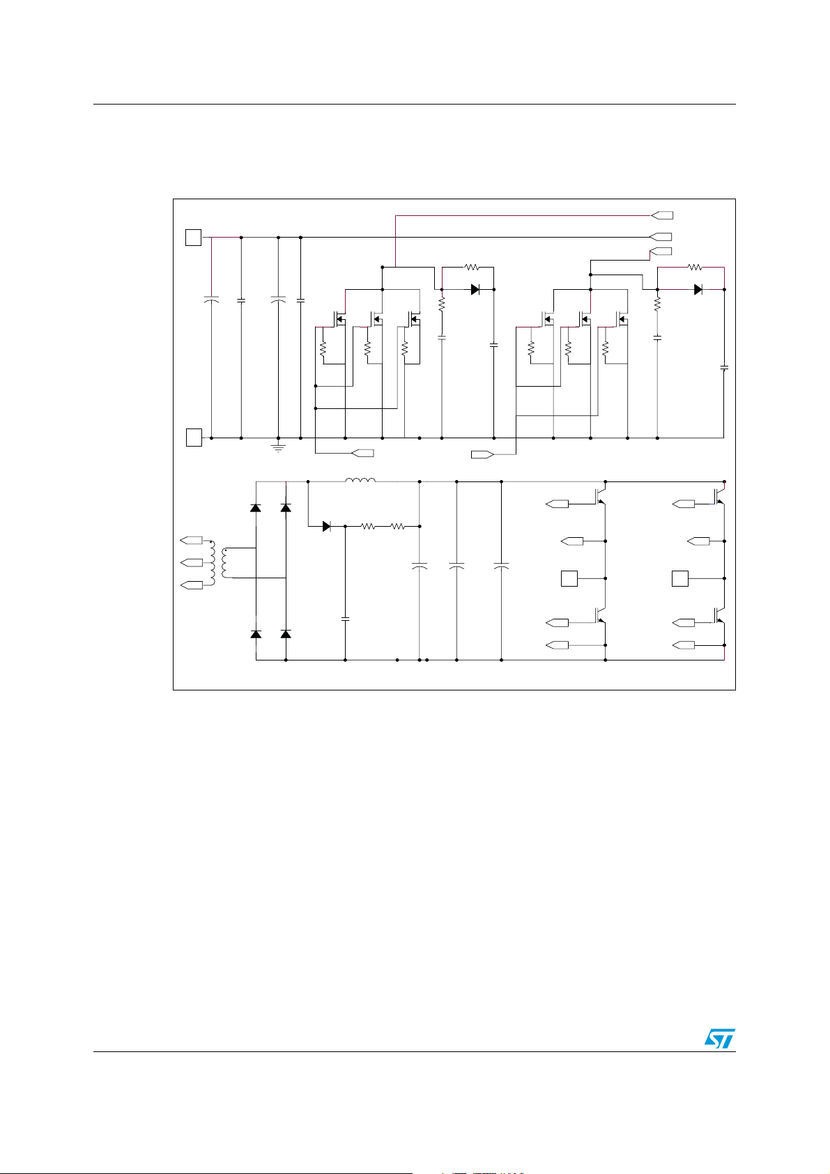
Circuit schematics STEVAL-ISV001V1
GND
C3
1 Circuit schematics
Figure 1. Converter schematic: the power stage
VIN
C38
D1
D4
D2
D3
D13
R92
M1
R91
GATE A
R94
R95
C34 C35 C36
C53
R96
D14
R2
C7
R90 R87
GATE B
G H 1
S H1
G L1
V A
R88
Igbt1
1
Igbt4
M5
M6 M4
G H2
G L 2
T1
T2
R1
C8
V AC 2
R97
D15
Igbt2
Igbt3
2/6
AM00632v1
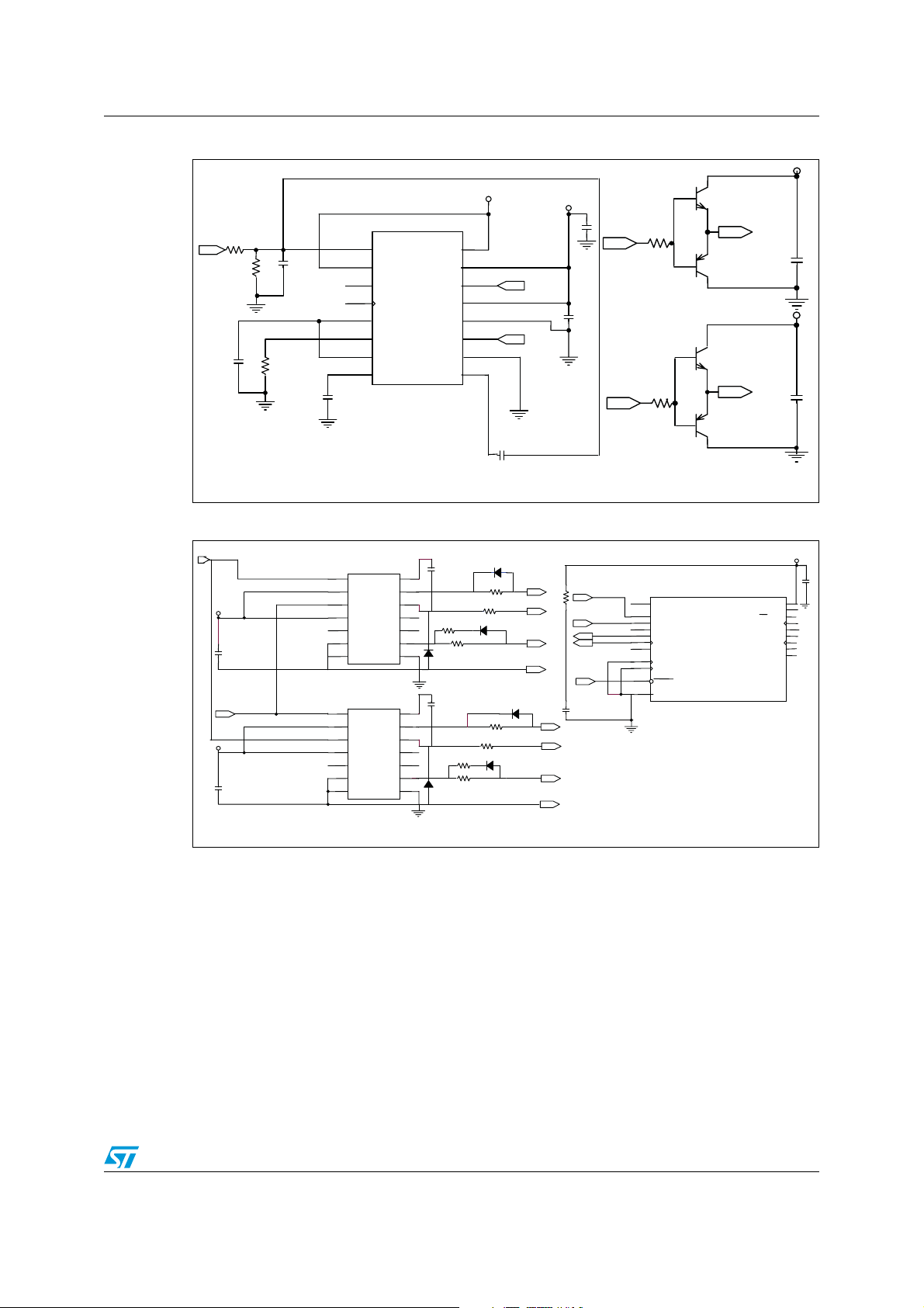
STEVAL-ISV001V1 Circuit schematics
_
_
Figure 2. Schematic of the push-pull control and driving circuit
VOUT
C11
R7
R9
R93
C16
C12
5u
1
2
3
4
5
6
7
8
U1
IN -
IN+
SYNC
OSC
CT
RT
DISCH
SS
SG3525
VREF
+VI
OUTB
VC
GND
OUTA
S.DOWN
COMP
+15V
16
15
14
PWM B
C10
+15V
PWM A
R20
Q9
2SD882
Q11
BC178B
13
12
11
PWM A
10
9
C14
Q10
BC107B
R21
Q12
BC178B
C17
0
PWM B
1n
+15V
GATE A
C18
+15V
C19
GATE B
0
AM00633v1
0
Figure 3. Inverter control driving circuit schematic
PWM LOW1/HIGH2
+15
C2
PWM LOW2/HIGH1
+15
C33
IC L6386
1
LIN
2
SD
3
HIN
4
VCC
5
DIAG
6
CIN
7
SG N
IC L6386
1
LIN
2
SD
3
HIN
4
VCC
DIAG 5NC
6
CIN
7
SGN
VBOOT
HVG
OUT
NC
NC
LV
GND
VBOOT
HVG
OUT
NC
LV
GND
R23
RG L1
R25
RG L 2
D6
RG H2
R24
D5
RG 1
R22
G H1
S H1
S L1
D7
D8
G H2
S H2
G L2
S L2
PWM LOW1/HIGH2
R9
PWM LOW2/HIGH1
PA5
PA6
RESET
C56
U1
18
PA0/LTI
17
PA1/ATI
16
PA2/ATPW
15
PA3/ATPW
14
PA4/ATPW
13
PA5/ATPWM3/ICCD
12
PA6/MCO/ICCCLK/BR
11
PA
20
OSC1/CLK
19
OSC
3
RESE
1
VS
ST7FLITE39
SOIC
C26
1
1
1
1
1
9
8
D9
0
C3
1
1
1
1
1
9
8
D10
0
PB0/SS/AI
PB1/SCK/AI
PB2/MISO/AI
PB3/MOSI/AI
PB4/CLKIN/AI
PB5/AIN
PB6/AIN
AM00634v1
5V
C57
2
VD
4
5
6
7
8
9
1
3/6

Circuit schematics STEVAL-ISV001V1
Figure 4. Schematic of the auxiliary power supply section
D12
C39
L3
150uH
U2
G
VIN
VOUT
N
L7805
2
SYN
COM
OU
IN
U1
+15V
C41
1
2
3
4
R81
C40
C5
D11
1
0
Vin
8
7
6
5
VC
GN
VRE
F
L5973D
R83
C51
+
+
C52
R82
C42
+
5V
Q8
3
C59
+15V
AM00635v1
4/6

STEVAL-ISV001V1 Revision history
2 Revision history
Table 1. Document revision history
Date Revision Changes
27-Nov-2008 1 Initial release.
5/6

STEVAL-ISV001V1
Please Read Carefully:
Information in this document is provided solely in connection with ST products. STMicroelectronics NV and its subsidiaries (“ST”) reserve the
right to make changes, corrections, modifications or improvements, to this document, and the products and services described herein at any
time, without notice.
All ST products are sold pursuant to ST’s terms and conditions of sale.
Purchasers are solely responsible for the choice, selection and use of the ST products and services described herein, and ST assumes no
liability whatsoever relating to the choice, selection or use of the ST products and services described herein.
No license, express or implied, by estoppel or otherwise, to any intellectual property rights is granted under this document. If any part of this
document refers to any third party products or services it shall not be deemed a license grant by ST for the use of such third party products
or services, or any intellectual property contained therein or considered as a warranty covering the use in any manner whatsoever of such
third party products or services or any intellectual property contained therein.
UNLESS OTHERWISE SET FORTH IN ST’S TERMS AND CONDITIONS OF SALE ST DISCLAIMS ANY EXPRESS OR IMPLIED
WARRANTY WITH RESPECT TO THE USE AND/OR SALE OF ST PRODUCTS INCLUDING WITHOUT LIMITATION IMPLIED
WARRANTIES OF MERCHANTABILITY, FITNESS FOR A PARTICULAR PURPOSE (AND THEIR EQUIVALENTS UNDER THE LAWS
OF ANY JURISDICTION), OR INFRINGEMENT OF ANY PATENT, COPYRIGHT OR OTHER INTELLECTUAL PROPERTY RIGHT.
UNLESS EXPRESSLY APPROVED IN WRITING BY AN AUTHORIZED ST REPRESENTATIVE, ST PRODUCTS ARE NOT
RECOMMENDED, AUTHORIZED OR WARRANTED FOR USE IN MILITARY, AIR CRAFT, SPACE, LIFE SAVING, OR LIFE SUSTAINING
APPLICATIONS, NOR IN PRODUCTS OR SYSTEMS WHERE FAILURE OR MALFUNCTION MAY RESULT IN PERSONAL INJURY,
DEATH, OR SEVERE PROPERTY OR ENVIRONMENTAL DAMAGE. ST PRODUCTS WHICH ARE NOT SPECIFIED AS "AUTOMOTIVE
GRADE" MAY ONLY BE USED IN AUTOMOTIVE APPLICATIONS AT USER’S OWN RISK.
Resale of ST products with provisions different from the statements and/or technical features set forth in this document shall immediately void
any warranty granted by ST for the ST product or service described herein and shall not create or extend in any manner whatsoever, any
liability of ST.
ST and the ST logo are trademarks or registered trademarks of ST in various countries.
Information in this document supersedes and replaces all information previously supplied.
The ST logo is a registered trademark of STMicroelectronics. All other names are the property of their respective owners.
© 2008 STMicroelectronics - All rights reserved
STMicroelectronics group of companies
Australia - Belgium - Brazil - Canada - China - Czech Republic - Finland - France - Germany - Hong Kong - India - Israel - Italy - Japan -
Malaysia - Malta - Morocco - Singapore - Spain - Sweden - Switzerland - United Kingdom - United States of America
www.st.com
6/6
 Loading...