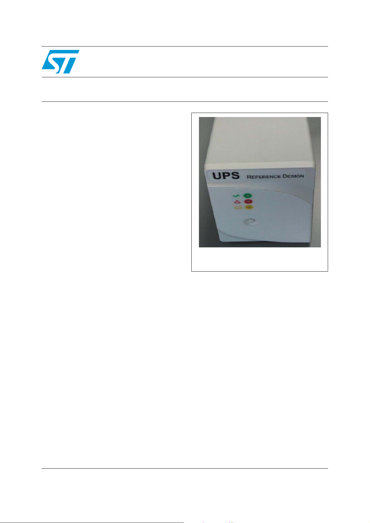
UPS reference design - 230 V / 50 Hz model
Features
■ Output rating power: 700 VA / 450 W
■ Input voltage: 160 Vac ± 3% - 294 Vac ± 3%
■ Input frequency: 50 Hz
■ Output voltage: 184 - 265 Vac ± 3 Vac
■ Output frequency: 50 Hz ± 0.1 Hz
■ On battery output waveform: quasi-sine
(square wave)
■ Transfer time: Class 3 [EN62040-3]
■ Typical recharge time: 8 h
■ Backup time (full load): 2.5 - 3 min.
■ Battery quantity: 2 pieces
■ Battery nominal voltage: 12 V
■ Battery capacity: 7.2 Ah
■ Battery recharge: two steps
■ Operating temperature: 0 °C to +40 °C
■ Storage temperature: -20 °C to +60 °C
■ Size (H x W x D): 175 mm x 120 mm x 430 mm
■ Weight: 11 kg
■ Shipping weight: 11.5 kg
■ EMI Classification: EN 62040-2
STEVAL-ISS001V2
Line interactive 450 W
Data Brief
STEVAL-ISS001V2
The UPS was designed with RS-232 joint signal
and USB interfaces (USB for RS-232 converter). It
is possible to connect the UPS to a PC using an
RS-232 or USB cable and control the UPS status
through the "UPS Monitor 3.0x" software that
must be installed on the same PC.
Description
This UPS reference design was built employing
off-line topology with AVR boost and buck
regulation of the mains. The inverter module
contains the push-pull DC-DC converter and the
DC-AC output full bridge generating a quasi-sine
waveform.
A microcontroller controls all UPS functions. It
monitors the mains parameters (input/output
mains voltage and phase, output inverter voltage,
battery voltage, output current and output power)
in order to ensure the proper level of the output
voltage.
April 2008 Rev 1 1/4
For further information contact your local STMicroelectronics sales office.
www.st.com
4

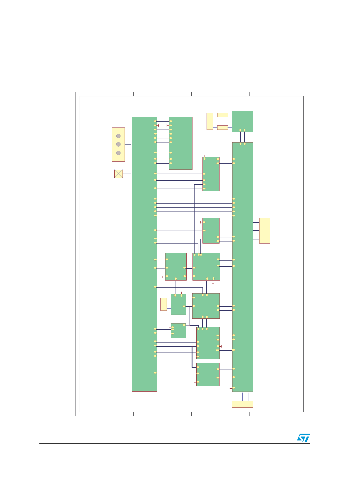
Board schematic STEVAL-ISS001V2
1 Board schematic
Figure 1. Schematic
B
M
i
c
r
o
cont
r
o
lle
r
L
E
D
IN
D
I
C
ATIO
NS
unit
B
UT
T
O
N
Mi
cr
oco
nt
ro
l
ler12st05v03
1
.s
ch
BAT_LOW
ACF1!
UPS_OFF!
USB_IN!
INP_LEV
PHASE
ACH!
OUT_REL!
OUT_LEV
INV_A
INV_B
VDCDC
CHOFF
AKK_LEV
VCCPU
ON/OFF
SW_ONP
PWR_LEV
VCC
GND
ACF!
TXD
RXD
VCC
ACI!
ACF
ACL!
SHD
VCC
VCC
VCC
GN
GND
D
BAT_LOW
ACF!
ACF1!
UPS_OFF!
USB_IN!
TXD
RXD
DCDC12st05v031.sch
VDCDC
SHD
G
N
D
CHOFF
BATTER
Y
BatOver12st05v031.sch
BatteryVoltage12st05v031.sch
G
ND
VCC
AKK_LEV
VCCPU
VCC
ON/OFF
SW_ONP
PWR_LEV
VDCDC
SHD
GND
VCC
GND
BAT_LOW
ACF!
ACF1!
UPS_OFF!
USB_IN!
TXD
RXD
INP_LEV
VCC
PHASE
ACI!
ACF
ACL!
ACH!
OUT_REL!
OUT_LEV
INV_A
INV_B
V
A
KK
HVDC
VAKK
VDD
VAKK
VBAT
VBAT
GND
VCC
AKK_LEV
DC/DC converter
HVDC
VDD
GN
Battery Overcurrent Protection
D
GND
GND
Battery Voltage
I
I
nter
n
erfac
f
ace1
e
2
s
u
t05v031
n
it
.s
ch
VDD
InputVoltage12st05v031.sch
InverterVoltage12st05v031.sch
GND
INV_A
INV_B
VDD
HVDC
VDD
GND
VBAT
VBAT
Power
VB
Suppl
A
T
y
VCCPU
VCC
ON/OFF
SW_ONP
PowerSupply12st05v031.sch
VCC
PWR_LEV
GND
GND
Output Current Measurement
OutputCurrent12st05v031.sch
I
N
P
UT
GND
AC_IN2
G
N
D
AC_IN1
INP_LEV
VCC
VDD
PHASE
GND
OUT_LEV
AC_1
AC_2
DCAC12st05v031.sch
INV_OUT2
INV_OUT1
VDD
GND
VDD
GND
VDD
CHOFF
AC_1
+V
VDD
OUT
AC_2
+VOUT
VD
D
V
+
VOUT
DD
AC_IN1
AC_IN2
GND
VPP
IOUT_1
IOUT_2
C
FUSE
FUSE
I
n
p
u
t
V
o
lt
a
ge
&
P
has
e
Me
as
ureme
n
t
Output Voltage Inverter
A
C
/
DC
C
harger
AC_IN1
AC_IN2
D
C/AC
I
n
vv
ert
er
AC_IN1
AC_IN2
GND
AC_1
AC_2
ACDC12
s
t
0
5v0
3
1.sch
IOUT_1
IOUT_2
AC_1
AC_2
RFIEMI12st05v031.sch
R
el
ays1
2s
t
05
v
03
1.s
ch
G
ND
AC_IN2
AC_
I
N2
A
C
_I
N
2
AC_IN1
AC_IN2
ACI!
ACF
ACL!
ACH!
OUT_REL!
AC_1
AC_2
INV_OUT2
INV_OUT1
AC_1
AC_2
AC_IN1
AC_IN2
VPP
IOUT_1
IOUT_2
GND
EMI/RFI FI
A
C_
L
I
N1
T
ER
AC_IN1
P
o
w
e
AC
r
R
_
IN
ela
1
ys
D
1
AVR TRAFO
8
B
2/4
OUTPUT
C
D

STEVAL-ISS001V2 Revision history
2 Revision history
Table 1. Document revision history
Date Revision Changes
14-Apr-2008 1 Initial release.
3/4

STEVAL-ISS001V2
Please Read Carefully:
Information in this document is provided solely in connection with ST products. STMicroelectronics NV and its subsidiaries (“ST”) reserve the
right to make changes, corrections, modifications or improvements, to this document, and the products and services described herein at any
time, without notice.
All ST products are sold pursuant to ST’s terms and conditions of sale.
Purchasers are solely responsible for the choice, selection and use of the ST products and services described herein, and ST assumes no
liability whatsoever relating to the choice, selection or use of the ST products and services described herein.
No license, express or implied, by estoppel or otherwise, to any intellectual property rights is granted under this document. If any part of this
document refers to any third party products or services it shall not be deemed a license grant by ST for the use of such third party products
or services, or any intellectual property contained therein or considered as a warranty covering the use in any manner whatsoever of such
third party products or services or any intellectual property contained therein.
UNLESS OTHERWISE SET FORTH IN ST’S TERMS AND CONDITIONS OF SALE ST DISCLAIMS ANY EXPRESS OR IMPLIED
WARRANTY WITH RESPECT TO THE USE AND/OR SALE OF ST PRODUCTS INCLUDING WITHOUT LIMITATION IMPLIED
WARRANTIES OF MERCHANTABILITY, FITNESS FOR A PARTICULAR PURPOSE (AND THEIR EQUIVALENTS UNDER THE LAWS
OF ANY JURISDICTION), OR INFRINGEMENT OF ANY PATENT, COPYRIGHT OR OTHER INTELLECTUAL PROPERTY RIGHT.
UNLESS EXPRESSLY APPROVED IN WRITING BY AN AUTHORIZED ST REPRESENTATIVE, ST PRODUCTS ARE NOT
RECOMMENDED, AUTHORIZED OR WARRANTED FOR USE IN MILITARY, AIR CRAFT, SPACE, LIFE SAVING, OR LIFE SUSTAINING
APPLICATIONS, NOR IN PRODUCTS OR SYSTEMS WHERE FAILURE OR MALFUNCTION MAY RESULT IN PERSONAL INJURY,
DEATH, OR SEVERE PROPERTY OR ENVIRONMENTAL DAMAGE. ST PRODUCTS WHICH ARE NOT SPECIFIED AS "AUTOMOTIVE
GRADE" MAY ONLY BE USED IN AUTOMOTIVE APPLICATIONS AT USER’S OWN RISK.
Resale of ST products with provisions different from the statements and/or technical features set forth in this document shall immediately void
any warranty granted by ST for the ST product or service described herein and shall not create or extend in any manner whatsoever, any
liability of ST.
ST and the ST logo are trademarks or registered trademarks of ST in various countries.
Information in this document supersedes and replaces all information previously supplied.
The ST logo is a registered trademark of STMicroelectronics. All other names are the property of their respective owners.
© 2008 STMicroelectronics - All rights reserved
STMicroelectronics group of companies
Australia - Belgium - Brazil - Canada - China - Czech Republic - Finland - France - Germany - Hong Kong - India - Israel - Italy - Japan -
Malaysia - Malta - Morocco - Singapore - Spain - Sweden - Switzerland - United Kingdom - United States of America
www.st.com
4/4
 Loading...