

Dual USB/wall adapter Li-Ion battery charger with gas gauge
demonstration board based on the STw4102
Features
■ Constant current constant voltage (CCCV)
charger
■ Dual charging source (main adaptor or USB
cable)
■ Fast charge current control up to 1A for main
adaptor and up to 500 mA for USB
■ Internal power device and sense resistor,
option for external components for current
higher than 1A
■ Programmable charge voltage (4.1 V, 4.2 V,
4.3 V, 4.35 V) with 1% accuracy
■ Thermal regulation
■ Trickle charge mode at low battery voltage
■ Main adaptor voltage up to 16 V
■ Battery overvoltage protection at 4.7 V
■ Gas gauge with 13 bit AD converter
■ Battery voltage monitor with 7-12 bit ADC
2
■ I
C interface for device monitoring and control
■ Charge status output pin
■ Power detection output pin
■ Programmable watchdog security timer
■ 4.7 V LDO regulator (external MOSFET)
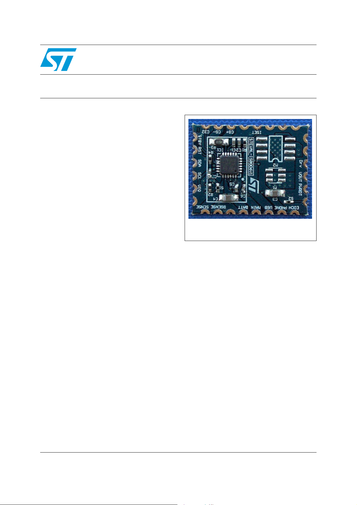
STEVAL-ISB006V1
Data Brief
STEVAL-ISB006V1
current against the die high power dissipation or
high ambient temperature. An end of charge
output pin indicates the charge termination when
the fast charge current drops below 10% of the
programmed current value. The STw4102
contains an accurate gas gauge based on a 13 bit
AD converter. External resistor is used between
battery and ground to sense a charge/discharge
current. With a typical 30 mΩ resistor, current can
be up to 2.5 A.
Description
The STEVAL-ISB006V1 demonstration board is
based on the STw4102, a stand-alone constantcurrent constant-voltage (CCCV) linear charger
dedicated for Li-Ion battery. This device allows
dual charging capability using the main input
adaptor up to 1A (wall adaptor, car adaptor) or
USB cable up to 500 mA without external
component. Upper 1 A charging is possible by
adding just one external transistor. This
demonstration board offers programmable fast
charge current up to 1A with external resistor. A
thermal regulation circuitry limits the charge
November 2008 Rev 1 1/4
For further information contact your local STMicroelectronics sales office.
www.st.com
4
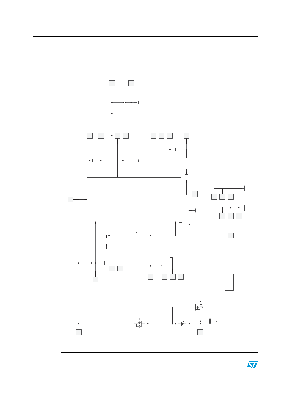
Circuit schematic STEVAL-ISB006V1
1 Circuit schematic
Figure 1. Schematic
1
BATT
VOUT
SENSE
1
1
Vbat
S1
0R
19
2
VOUT
SENSE
1
Drv
Driver
4
USBPWR
MAIN
IC1
3
1
21
20
BATT
PWRDETECTN
24
R2
10K
Vbat
BSENSE C4
1
BATTSENSE
22
22uF/6.3V/X5R
7
ISET
EOCHG
8
1
GNDBATT
ISET
1
12K +/-1%
R1
10
CV IS
STw4102
CVREF
C2
1uF/6.3V/X5R
C1
LDODRV5LDOFB
6
CG+
STBY
C32
1
1
1uF/6.3V/X5R
13
C32kHz
R4
C7
14
VIO
18
10K
100nF/16V/X7R
1
11
ICG+
STDBY
SDA16RESETN
SCL
17
CG-
1
R3
R033 +/-1% 0805
12
S2
0R
ICG-
TEST
GND
15
TEST
1
23
9
Epad
1
GND101GND11
1
GND12
1
1
GND6
1
GND8
GND7
1
GND3
1
C5
C6
1
100nF/16V/X7R
100nF/16V/X7R
USB
1
MAIN
1
EOCH
PWRDT
M2B
STS2DPFS20V
2/4
1
1
VIO
1
1
RST
SDA
SCL
BL1
LOGO_PCB
M1
STT4PF20V
M2A
STS2DPFS20V
C3
1
22uF/6.3V/X5R
PHONE
AM03287v1
STEVAL-ISB006V1 Revision history
2 Revision history
Table 1. Document revision history
Date Revision Changes
27-Nov-2008 1 Initial release.
3/4

STEVAL-ISB006V1
Please Read Carefully:
Information in this document is provided solely in connection with ST products. STMicroelectronics NV and its subsidiaries (“ST”) reserve the
right to make changes, corrections, modifications or improvements, to this document, and the products and services described herein at any
time, without notice.
All ST products are sold pursuant to ST’s terms and conditions of sale.
Purchasers are solely responsible for the choice, selection and use of the ST products and services described herein, and ST assumes no
liability whatsoever relating to the choice, selection or use of the ST products and services described herein.
No license, express or implied, by estoppel or otherwise, to any intellectual property rights is granted under this document. If any part of this
document refers to any third party products or services it shall not be deemed a license grant by ST for the use of such third party products
or services, or any intellectual property contained therein or considered as a warranty covering the use in any manner whatsoever of such
third party products or services or any intellectual property contained therein.
UNLESS OTHERWISE SET FORTH IN ST’S TERMS AND CONDITIONS OF SALE ST DISCLAIMS ANY EXPRESS OR IMPLIED
WARRANTY WITH RESPECT TO THE USE AND/OR SALE OF ST PRODUCTS INCLUDING WITHOUT LIMITATION IMPLIED
WARRANTIES OF MERCHANTABILITY, FITNESS FOR A PARTICULAR PURPOSE (AND THEIR EQUIVALENTS UNDER THE LAWS
OF ANY JURISDICTION), OR INFRINGEMENT OF ANY PATENT, COPYRIGHT OR OTHER INTELLECTUAL PROPERTY RIGHT.
UNLESS EXPRESSLY APPROVED IN WRITING BY AN AUTHORIZED ST REPRESENTATIVE, ST PRODUCTS ARE NOT
RECOMMENDED, AUTHORIZED OR WARRANTED FOR USE IN MILITARY, AIR CRAFT, SPACE, LIFE SAVING, OR LIFE SUSTAINING
APPLICATIONS, NOR IN PRODUCTS OR SYSTEMS WHERE FAILURE OR MALFUNCTION MAY RESULT IN PERSONAL INJURY,
DEATH, OR SEVERE PROPERTY OR ENVIRONMENTAL DAMAGE. ST PRODUCTS WHICH ARE NOT SPECIFIED AS "AUTOMOTIVE
GRADE" MAY ONLY BE USED IN AUTOMOTIVE APPLICATIONS AT USER’S OWN RISK.
Resale of ST products with provisions different from the statements and/or technical features set forth in this document shall immediately void
any warranty granted by ST for the ST product or service described herein and shall not create or extend in any manner whatsoever, any
liability of ST.
ST and the ST logo are trademarks or registered trademarks of ST in various countries.
Information in this document supersedes and replaces all information previously supplied.
The ST logo is a registered trademark of STMicroelectronics. All other names are the property of their respective owners.
© 2008 STMicroelectronics - All rights reserved
STMicroelectronics group of companies
Australia - Belgium - Brazil - Canada - China - Czech Republic - Finland - France - Germany - Hong Kong - India - Israel - Italy - Japan -
Malaysia - Malta - Morocco - Singapore - Spain - Sweden - Switzerland - United Kingdom - United States of America
www.st.com
4/4
 Loading...