

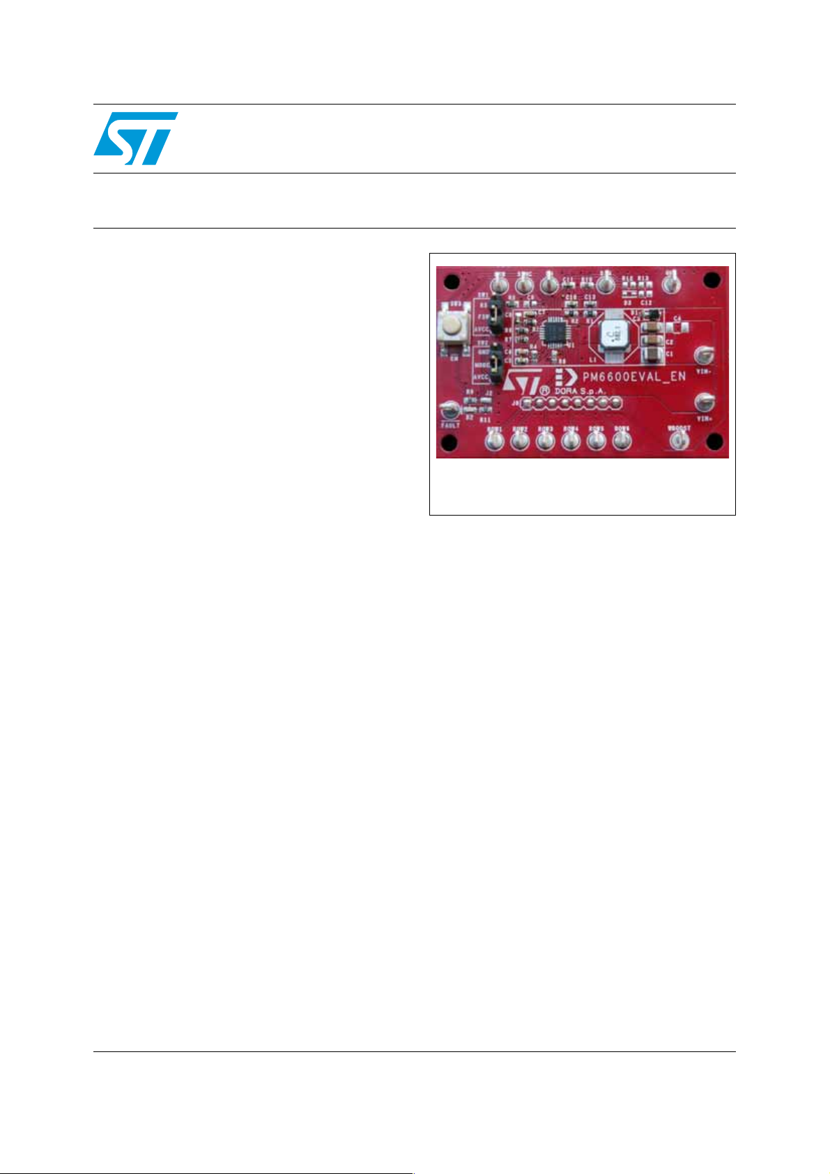
STEVAL-ISA056V1
6 rows - 30 mA LEDs driver with boost converter for LCD panels
backlight evaluation board based on the PM6600
Features
■ Boost section
– 4.5 V to 28 V input voltage range
– Internal Power MOSFET
– Internal +5 V LDO for device supply
– Up to 36 V outp ut voltage
– Constant frequency peak current-mode ctrl
– 200 kHz to 1 MHz adjustable switching
frequency
– External sync for multi-device application
– Pulse-skip power saving mode at light load
– Programmable soft-start
– Programmable OVP protection
– Single ceramic output capacitor
– Latched thermal shutdown
■ Backlight driver section
– Six rows with 30mA maximum current
capability (adjustable)
– Up to 10 W LEDs per row
– Rows disable option
– Less than 500 ns minimum dimming time
(1% minimum dimming duty-cycle at 20
kHz dimming frequency)
– ±2.0% current matching between rows
– LED failure (open and short circuit)
detection
managed). The device allows to detect and
manage the open and shorted LED faults and to
let unused rows floating. Basic protections
(output over-voltage, internal MOSFET overcurrent and thermal shutd own) are pr ovided.
STEVAL-ISA056V1
Data Brief
Description
This evaluation board based on the PM6600
consists of a high efficiency monolithic boost
converter and six controlled current generators
(rows) specifically designed to supply LEDs
arrays used in the backlight of LCD panels. The
device can manage an output voltage up to 36 V
(i.e. ten white-LEDs per ro w).
The generators can be externally programmed to
sink up to 30 mA and can be dimmed via a PWM
signal (1% dimming duty-cycle at 20 kHz can be
March 2008 Rev 1 1/4
For further information contact your local STMicroelectronics sales office .
www.st.com
4
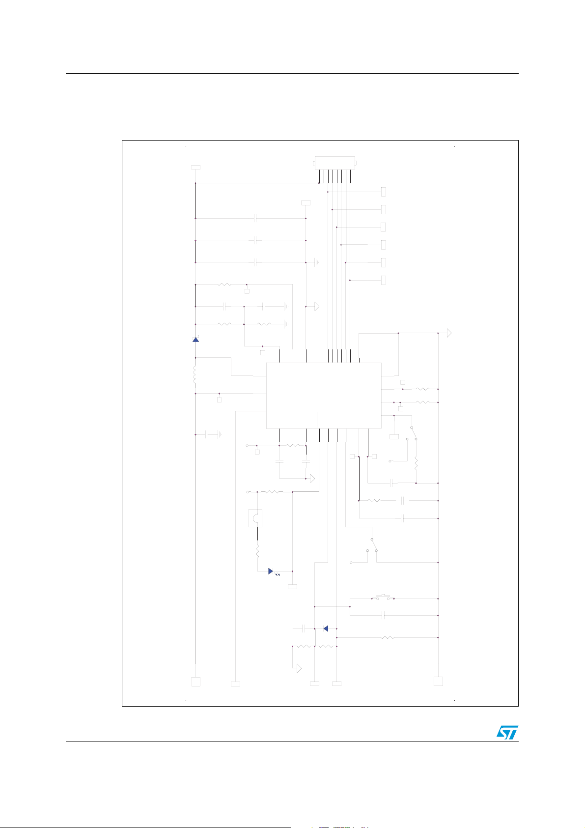
Circuit schematic STEVAL-ISA056V1
AV
PG
OVSE
DI
660
EA
R
IN
60
10
80
VBOOS
N.
IN
AV
DI
SLOP
N.
PS
10
D,
RI
OVSE
33
AV
AV
1 Circuit schematic
Figure 1. Schematic
T
VBOOS
TP7
8
7
456
8
J8
DER
HEA
3
1
2
GND
M.
C4
N.
C3
2u2
C2
2u2
k
R8
D1
680
p
E
C13
22p
R1
510k
1L40M
STPS
L1 6u8
VIN
C1
10u
C10
560
SLOP
R2
16k
L
OVSE
18
L
LX
19
OVSE
VIN
8
SYSYNC
23
AVCC
U1
6
CC
AV
CC
AV
0n
C6 10
AVCC
0k
R9
10
12
J2
LED_EN
3mA
R11 1k2
RED,
D2
TP8
12
15
9
17
16
ND
PG
SLOPE
25
11
14
13
THPD
ROW2
ROW5
ROW1
ROW4
ROW6
ROW3
0
PM660
M
DI
EN
LDO5
FAULT
7
22
4R7
R4
FAULT
21
C5 1u
D3
NM
C12
NM
COMP1MODE
5
20
COMP
CC
AV
ROW6
ROW5
ROW4
ROW3
ROW2
ROW1
SGSGND
10
BILIM
3
RIRILIM
2
FSW
4
SS
24
SS
CC
AV
C7
2k4
R3
SW2
MODE
RES
SW3
4n7
C11
R7
180k
BILIM
LIM
R6
51k
RI
SW1
FSW
TP13
FSW
0k
R5 33
3n3
C8
4n7
M.
C9
N.
100k
+
VIN
SYNC
R12
NM
R13
NM
M
EN
DI
R10
-
VIN
2/4

STEVAL-ISA056V1 Revision history
2 Revision history
Table 1. Document revision history
Date Revision Changes
10-Mar-2008 1 Initial release.
3/4

STEVAL-ISA056V1
y
Please Read Carefully:
Information in this document is provided solely in connection with ST products. STMicroelectronics NV and its subsidiaries (“ST”) reserve the
right to make changes, corrections, modifications or improvements, to this document, and the products and services described herein at any
time, without notice.
All ST products are sold pursuant to ST’s terms and conditions of sale.
Purchasers are solely res ponsibl e fo r the c hoic e, se lecti on an d use o f the S T prod ucts and s ervi ces d escr ibed he rein , and ST as sumes no
liability whatsoever relati ng to the choice, selection or use of the ST products and services described herein.
No license, express or implied, by estoppel or otherwise, to any intellectual property rights is granted under this document. If any part of this
document refers to any third pa rty p ro duc ts or se rv ices it sh all n ot be deem ed a lice ns e gr ant by ST fo r t he use of su ch thi r d party products
or services, or any intellectua l property c ontained the rein or consi dered as a warr anty coverin g the use in any manner whats oever of such
third party products or servi ces or any intellectual property contained therein.
UNLESS OTHERWISE SET FORTH IN ST’S TERMS AND CONDITIONS OF SALE ST DISCLAIMS ANY EXPRESS OR IMPLIED
WARRANTY WITH RESPECT TO THE USE AND/OR SALE OF ST PRODUCTS INCLUDING WITHOUT LIMITATION IMPLIED
WARRANTIES OF MERCHANTABILITY, FITNESS FOR A PARTICUL AR PURPOS E (AND THEIR EQUIVALE NTS UNDER THE LAWS
OF ANY JURISDICTION), OR INFRINGEMENT OF ANY PATENT, COPYRIGHT OR OTHER INTELLECTUAL PROPERTY RIGHT.
UNLESS EXPRESSLY APPROVED IN WRITING BY AN AUTHORIZED ST REPRESENTATIVE, ST PRODUCTS ARE NOT
RECOMMENDED, AUTHORIZED OR WARRANTED FOR USE IN MILITARY, AIR CRAFT, SPACE, LIFE SAVING, OR LIFE SUSTAINING
APPLICATIONS, NOR IN PRODUCTS OR SYSTEMS WHERE FAILURE OR MALFUNCTION MAY RESULT IN PERSONAL INJ URY,
DEATH, OR SEVERE PROPERTY OR ENVIRONMENTAL DAMAGE. ST PRODUCTS WHICH ARE NOT SPECIFIED AS "AUTOMOTIVE
GRADE" MAY ONLY BE USED IN AUTOMOTIVE APPLICATIONS AT USER’S OWN RISK.
Resale of ST products with provisions different from the statements and/or technical features set forth in this document shall immediately void
any warranty granted by ST fo r the ST pro duct or serv ice describe d herein and shall not cr eate or exten d in any manne r whatsoever, an
liability of ST.
ST and the ST logo are trademarks or registered trademarks of ST in various countries.
Information in this document su persedes and replaces all information previously supplied.
The ST logo is a registered trademark of STMicroelectronics. All other names are the property of their respective owners.
© 2008 STMicroelectronics - All rights reserved
STMicroelectronics group of compan ie s
Australia - Belgium - Brazil - Canada - China - Czech Republic - Finland - France - Germany - Hong Kong - India - Isra el - Italy - Japan -
Malaysia - Malta - Morocco - Singapore - Spain - Sweden - Switzerland - United Kingdom - United States of America
www.st.com
4/4
 Loading...