

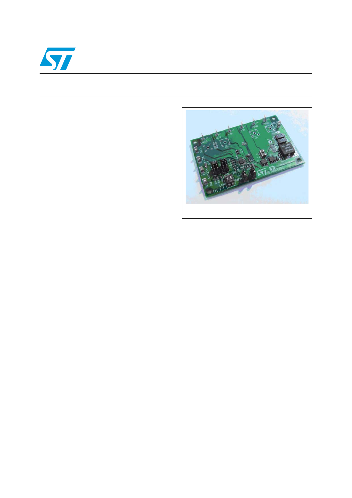
Evaluation board for the PM6675AS high efficiency
step-down controller with embedded 2 A LDO regulator
Features
■ 4.5 V to 36 V input voltage range
■ 0.6 V, ±1% voltage reference
■ 1.5 V fixed output voltage
■ 0.6 V to 3.3 V adjustable output voltage
■ 1.237 V ±1% reference voltage available
■ Very fast load transient response using
constant on-time (COT) control loop
■ No RSENSE current sensing using R
the low-side MOSFETs
■ Negative current limit
■ Latched OVP, UVP and thermal shutdown
■ Fixed 3 ms soft-start
■ Selectable pulse-skipping at light load
■ Selectable no-audible (33 kHz) pulse-skip
mode
■ All ceramic output capacitors application
supported
■ Output voltage ripple compensation
■ Output soft-end
DS(ON)
STEVAL-ISA052V2
Data Brief
of
STEVAL-ISA052V2
and source up to 2 Apk. Two fixed current limits
(±1 A and ±2 A) can be chosen.
An active soft-end is independently performed on
both the switching and the linear regulator outputs
when disabled.
Description
This evaluation board is based on the PM6675AS
device, which consists of a single high efficiency
step-down controller and an independent lowdropout (LDO) linear regulator.
The constant on-time (COT) architecture assures
fast transient response supporting both
electrolytic and ceramic output capacitors. An
embedded integrator control loop compensates
the DC voltage error due to the output ripple.
Selectable low-consumption mode allows the
highest efficiency over a wide range of load
conditions. The low-noise mode sets the minimum
switching frequency to 33 kHz for audio-sensitive
applications. The LDO linear regulator can sink
May 2008 Rev 1 1/4
For further information contact your local STMicroelectronics sales office.
www.st.com
4
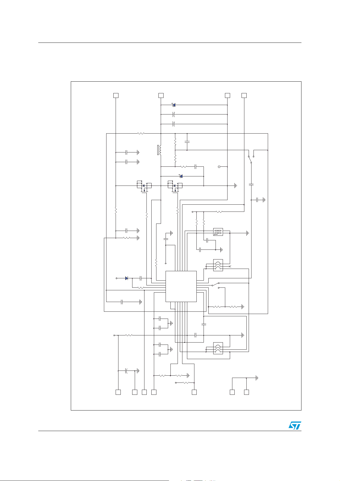
Circuit schematic STEVAL-ISA052V2
VSE
66
SP
VSE
AV
SK
BA
22
SP
VE
SK
PS
1 Circuit schematic
Figure 1. Schematic diagram
VIN
J1
1
R6
0
C2
10u
12
0 0
12
10u
C1
2x UMK325BJ106KM-T
8
7
6
5
Q1
R1 330k
1 2
C14
100n
0
12
12
R2
18k
T54J
D1
BA
VCC
21
C11
10u
12
12
R10
C12
0
0
VOUT
J2
2x 4TPE220MF
L1 0. 9u
MLC1240-901ML
S12NH3LL
3
2
1
4
R4 3R3
1 2
1 2
100n
1L30A
STPS
1
D3
2 1
0u
22
C4
12
C3
220u
12
1 2
C15 6.8n
1 2
R14 7.5k R15 6. 8k
8
7
6
5
Q2
4
R17 0
100n
C13
0
1 2
R3 1.2k
VCC
18
17
VCC
LGATE
CSNS
19
PHASASE
20
HGATE
21
BOOT
22
LIN
23
LOUT
24
U1
LGND
LFB
THPD
2
1
25
1n
R16
4R7
12
STPS1L30M
2 1
D2
3
2
1
S12NH3LL
VCC
R12 100k
R11 100k
1 2
1 2
12
12
C21
100p
16
13
15
14
G
LEN
SP
PGND
SWEN
LILIM
12
COMP
11
VSE
L
75S
10
VSVSNS
9
VOSC
PM66
8
VREF
IP
NOSK
3
4
7
CC
AV
SGND
LPG
6
5
C22
TP1
12
SW1
3
4
100p
JP2
JP3
R9
J3
GND_TP
R13
100k
2
1
0
5 6
3 4
1 2
13k
G
PGND
SP
J4
1
1
SR
INT-VE
JP5
0
1 2
C16 680p
0
12
C17
N.M.
LEN-SWEN
LILIM
L
VSE
R8
0
12k
0
R7
3R9
12
VCC
C5
1u
0 0
12
1
1
J10
J5
VCC
J6
VCCGND
2/4
C20
N.M.
12
0
N.M.
C19
12
10u
C7
12
0
10u
C6
12
10k
R20
7.5k
R19
1
1
J7
LIN
LOUT
VCC
R18
100k
12
C9
100n
C10
12
IP
NOSK
JP1
5 6
3 4
1 2
0
1 C18
J8
LPG
0
0
1
1
J11
J9
PGND
LGND
STEVAL-ISA052V2 Revision history
2 Revision history
Table 1. Document revision history
Date Revision Changes
05-May-2008 1 Initial release.
3/4

STEVAL-ISA052V2
y
Please Read Carefully:
Information in this document is provided solely in connection with ST products. STMicroelectronics NV and its subsidiaries (“ST”) reserve the
right to make changes, corrections, modifications or improvements, to this document, and the products and services described herein at any
time, without notice.
All ST products are sold pursuant to ST’s terms and conditions of sale.
Purchasers are solely responsible for the choice, selection and use of the ST products and services described herein, and ST assumes no
liability whatsoever relating to the choice, selection or use of the ST products and services described herein.
No license, express or implied, by estoppel or otherwise, to any intellectual property rights is granted under this document. If any part of this
document refers to any third party products or services it shall not be deemed a license grant by ST for the use of such third party products
or services, or any intellectual property contained therein or considered as a warranty covering the use in any manner whatsoever of such
third party products or services or any intellectual property contained therein.
UNLESS OTHERWISE SET FORTH IN ST’S TERMS AND CONDITIONS OF SALE ST DISCLAIMS ANY EXPRESS OR IMPLIED
WARRANTY WITH RESPECT TO THE USE AND/OR SALE OF ST PRODUCTS INCLUDING WITHOUT LIMITATION IMPLIED
WARRANTIES OF MERCHANTABILITY, FITNESS FOR A PARTICULAR PURPOSE (AND THEIR EQUIVALENTS UNDER THE LAWS
OF ANY JURISDICTION), OR INFRINGEMENT OF ANY PATENT, COPYRIGHT OR OTHER INTELLECTUAL PROPERTY RIGHT.
UNLESS EXPRESSLY APPROVED IN WRITING BY AN AUTHORIZED ST REPRESENTATIVE, ST PRODUCTS ARE NOT
RECOMMENDED, AUTHORIZED OR WARRANTED FOR USE IN MILITARY, AIR CRAFT, SPACE, LIFE SAVING, OR LIFE SUSTAINING
APPLICATIONS, NOR IN PRODUCTS OR SYSTEMS WHERE FAILURE OR MALFUNCTION MAY RESULT IN PERSONAL INJURY,
DEATH, OR SEVERE PROPERTY OR ENVIRONMENTAL DAMAGE. ST PRODUCTS WHICH ARE NOT SPECIFIED AS "AUTOMOTIVE
GRADE" MAY ONLY BE USED IN AUTOMOTIVE APPLICATIONS AT USER’S OWN RISK.
Resale of ST products with provisions different from the statements and/or technical features set forth in this document shall immediately void
any warranty granted by ST for the ST product or service described herein and shall not create or extend in any manner whatsoever, an
liability of ST.
ST and the ST logo are trademarks or registered trademarks of ST in various countries.
Information in this document supersedes and replaces all information previously supplied.
The ST logo is a registered trademark of STMicroelectronics. All other names are the property of their respective owners.
© 2008 STMicroelectronics - All rights reserved
STMicroelectronics group of companies
Australia - Belgium - Brazil - Canada - China - Czech Republic - Finland - France - Germany - Hong Kong - India - Israel - Italy - Japan -
Malaysia - Malta - Morocco - Singapore - Spain - Sweden - Switzerland - United Kingdom - United States of America
www.st.com
4/4
 Loading...