

Features
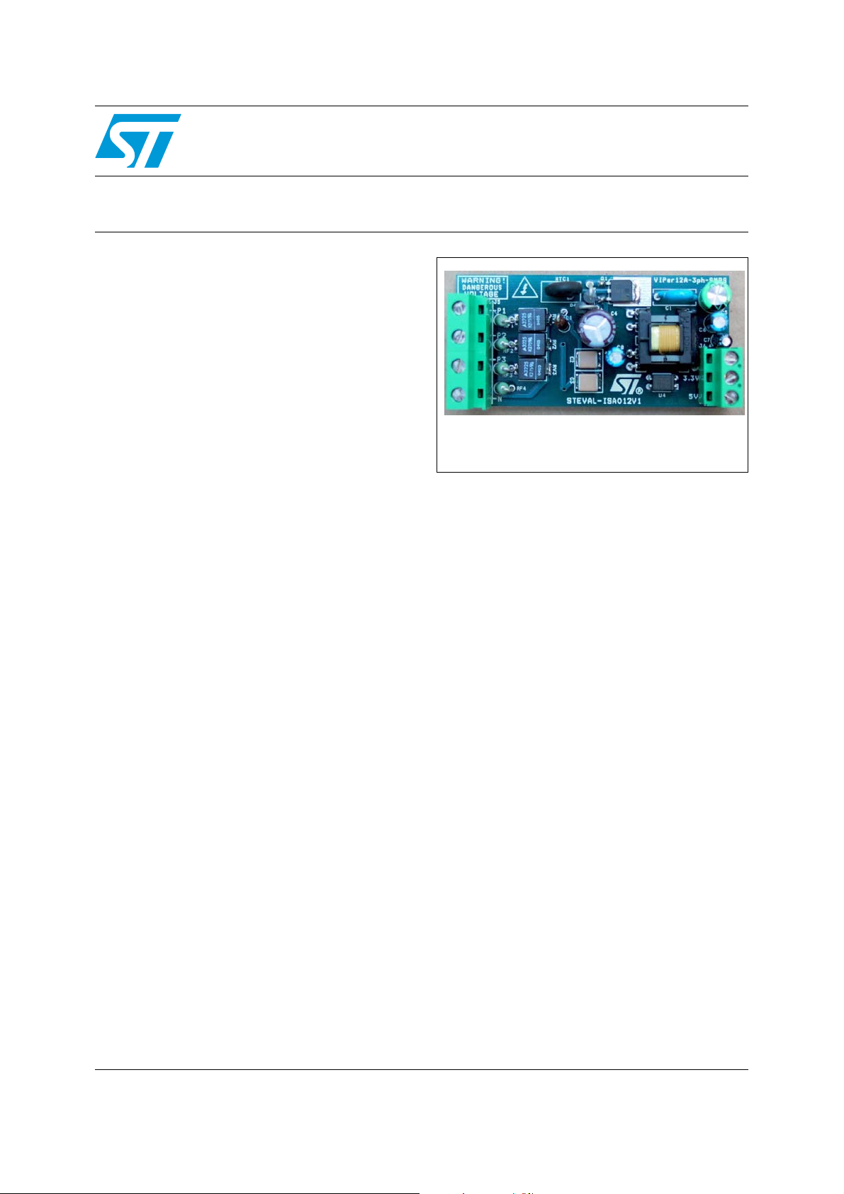
STEVAL-ISA012V1
3 phase power supply with VIPer and Power MOSFETs
Data Brief
■ Minimum AC input voltage = 90 V
■ Maximum AC input voltage = 450 V
■ Time of hold up capability > 50 ms
■ Mean input power < 6 W (in compliance with
AC
AC
IEC62053-21)
■ Input connections allowed:
– 1-phase with neutral
– 2-phase without neutral
– 3-phase with neutral
■ V
■ V
■ Maximum precision error = 3%
■ Maximum ripple voltage = 50 mV
■ Line regulation = +/- 1%
■ Load regulation = +/- 1%
■ Output power (peak) = 550 mW
OUT1
OUT2
= 5 V, I
OUT1
= 3.3 V, I
= 10 mA
= 100 mA
OUT2
Description
This reference design represents a cost effective
solution for low power high voltage power
supplies. It has been developed to cover
applications requiring an ultra-wide input voltage
range (between 90 and 450 V
phase applications. This requires the use of very
high voltage components, which increases cost,
size, weight and the overall complexity of the
power supply. The circuit includes a switching
transistor connected between the input rectifier
and the DC bulk capacitor (STMicroelectronics
patent). The series switch limits the DC input
voltage of the power converter by means of a
driving circuit; thus the SMPS primary transistor
can be selected as a standard part as well as a
smart power primary IC.
), typical of three-
AC
STEVAL-ISA012V1
Typical end applications for this solution can be
found in the industrial market in the range below 5
W, such as three-phase and single-phase power
meters, industrial bias power supplies and
auxiliary SMPS for high voltage street lighting,
where the input voltage can range from 90 V
450 V
and 1000 V Power MOSFETs are
AC
AC
to
currently used.
November 2007 Rev 1 1/4
For further information contact your local STMicroelectronics sales office.
www.st.com
4
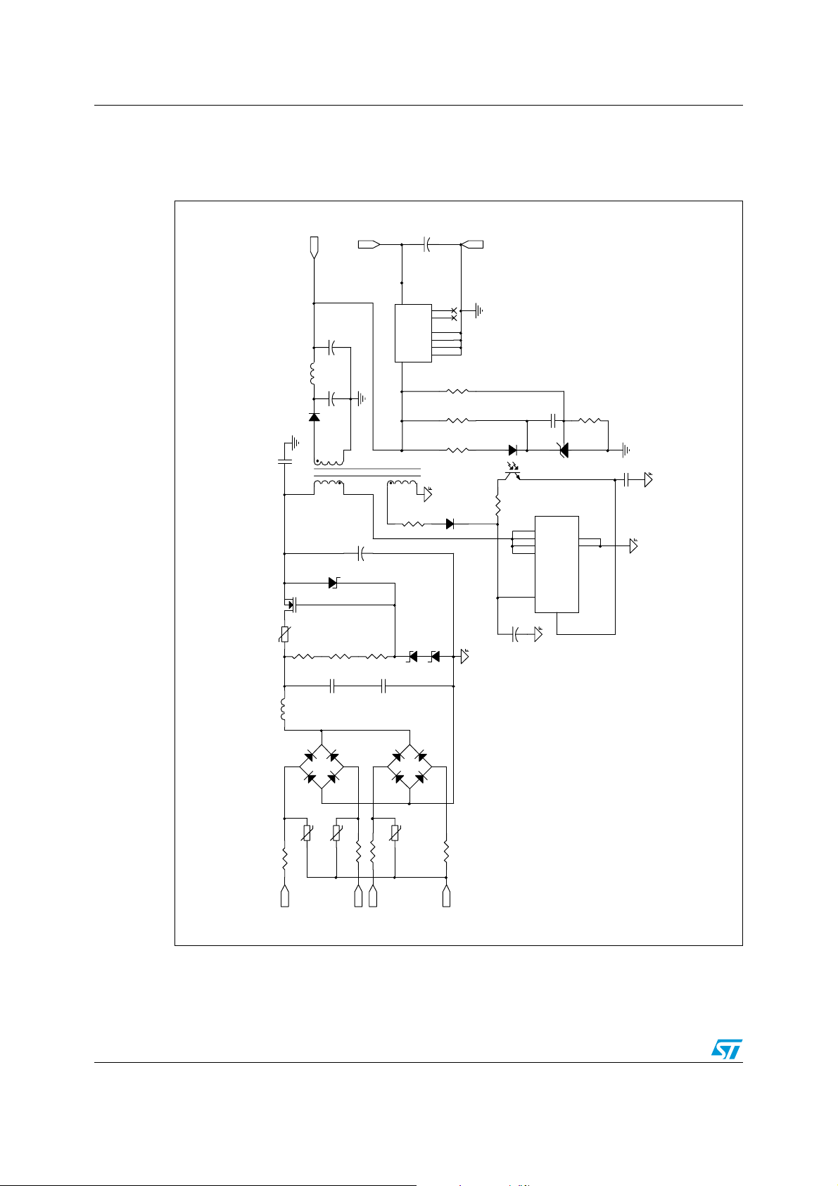
Board schematic STEVAL-ISA012V1
1 Board schematic
Figure 1. Schematic
3.3V@100mA
1
U2 L4931ABD33
8
4
+
R7
R6
R5
LL4148
GND
4.7K
SMD
1K
SMD
12
U4
PC817
43
220E SMD
R9
C8
50V
SMD
R8
TS2431
3
4.7K SMD
3
2 1
C10
47nF
50V
SMD
S
1
S
2
VIPer12AS
FB
C9
100nF
U3
5.6K SMD
D
8
D
7
D
6
D
5
U1
Vdd
4
+
10uF 50V
C7
2.2uF 25V
INH
5
NC
4
VOUT
GND
7
GND
6
GND
3
GND
2
VIN
5
D7
R4
10E
SMD
D4
180V
D3
180V
VDD
5V@10mA
L2
10uH 100mA SMD
D6
TMBAT49
C1
Q1
NTC1
10
2.2nF/ 2kV (Y1)
T1
1
D5
1
STD3NK50Z
2 3
50E
R1
3.3V
+
C6
22uF 25V
+
C5
330uF 25V
6
2
2.2uF450V
+
C4
SOD-80
ZMM 1 5
R3
330K SMD
330K SMD
R2
330K SMD
D1
2
RV1
SO5K275/275V
P1
C2
220nF
3
-+
4
RV2
SO5K275/275V
L1
1mH
RF1
22E 0.75W
630V
SMD
BRID GE
RF2
1
22E 0.75W
P2NP3
C3
630V
SMD
220nF
3
D2
2
-+
4
RV3
RF3
22E 0.75W
2/4
SO5K275/275V
BRID GE
1
RF4
22E 0.75W
Layout Hin ts: Q1 mounted on 1cm x 0.8cm copper
area. C8&C 10 have to be c losed to the VI Per12AS.
GND Pins f or U2 have to b e soldered to a unique
Note:
copper are a.

STEVAL-ISA012V1 Revision history
2 Revision history
Table 1. Document revision history
Date Revision Changes
28-Nov-2007 1 Initial release
3/4

STEVAL-ISA012V1
y
Please Read Carefully:
Information in this document is provided solely in connection with ST products. STMicroelectronics NV and its subsidiaries (“ST”) reserve the
right to make changes, corrections, modifications or improvements, to this document, and the products and services described herein at any
time, without notice.
All ST products are sold pursuant to ST’s terms and conditions of sale.
Purchasers are solely responsible for the choice, selection and use of the ST products and services described herein, and ST assumes no
liability whatsoever relating to the choice, selection or use of the ST products and services described herein.
No license, express or implied, by estoppel or otherwise, to any intellectual property rights is granted under this document. If any part of this
document refers to any third party products or services it shall not be deemed a license grant by ST for the use of such third party products
or services, or any intellectual property contained therein or considered as a warranty covering the use in any manner whatsoever of such
third party products or services or any intellectual property contained therein.
UNLESS OTHERWISE SET FORTH IN ST’S TERMS AND CONDITIONS OF SALE ST DISCLAIMS ANY EXPRESS OR IMPLIED
WARRANTY WITH RESPECT TO THE USE AND/OR SALE OF ST PRODUCTS INCLUDING WITHOUT LIMITATION IMPLIED
WARRANTIES OF MERCHANTABILITY, FITNESS FOR A PARTICULAR PURPOSE (AND THEIR EQUIVALENTS UNDER THE LAWS
OF ANY JURISDICTION), OR INFRINGEMENT OF ANY PATENT, COPYRIGHT OR OTHER INTELLECTUAL PROPERTY RIGHT.
UNLESS EXPRESSLY APPROVED IN WRITING BY AN AUTHORIZED ST REPRESENTATIVE, ST PRODUCTS ARE NOT
RECOMMENDED, AUTHORIZED OR WARRANTED FOR USE IN MILITARY, AIR CRAFT, SPACE, LIFE SAVING, OR LIFE SUSTAINING
APPLICATIONS, NOR IN PRODUCTS OR SYSTEMS WHERE FAILURE OR MALFUNCTION MAY RESULT IN PERSONAL INJURY,
DEATH, OR SEVERE PROPERTY OR ENVIRONMENTAL DAMAGE. ST PRODUCTS WHICH ARE NOT SPECIFIED AS "AUTOMOTIVE
GRADE" MAY ONLY BE USED IN AUTOMOTIVE APPLICATIONS AT USER’S OWN RISK.
Resale of ST products with provisions different from the statements and/or technical features set forth in this document shall immediately void
any warranty granted by ST for the ST product or service described herein and shall not create or extend in any manner whatsoever, an
liability of ST.
ST and the ST logo are trademarks or registered trademarks of ST in various countries.
Information in this document supersedes and replaces all information previously supplied.
The ST logo is a registered trademark of STMicroelectronics. All other names are the property of their respective owners.
© 2007 STMicroelectronics - All rights reserved
STMicroelectronics group of companies
Australia - Belgium - Brazil - Canada - China - Czech Republic - Finland - France - Germany - Hong Kong - India - Israel - Italy - Japan -
Malaysia - Malta - Morocco - Singapore - Spain - Sweden - Switzerland - United Kingdom - United States of America
www.st.com
4/4
 Loading...