Page 1

6W non-isolated fly-back topology power supply
Features
■ Switch mode general purpose power supply
■ Input: 90 to 264Vac @ 50/60Hz
■ Main Output (regulated): 5V, 500mA @ 50/
60Hz
■ Second output: 15V, 200mA
■ Output power (pick): 5.5W
Description
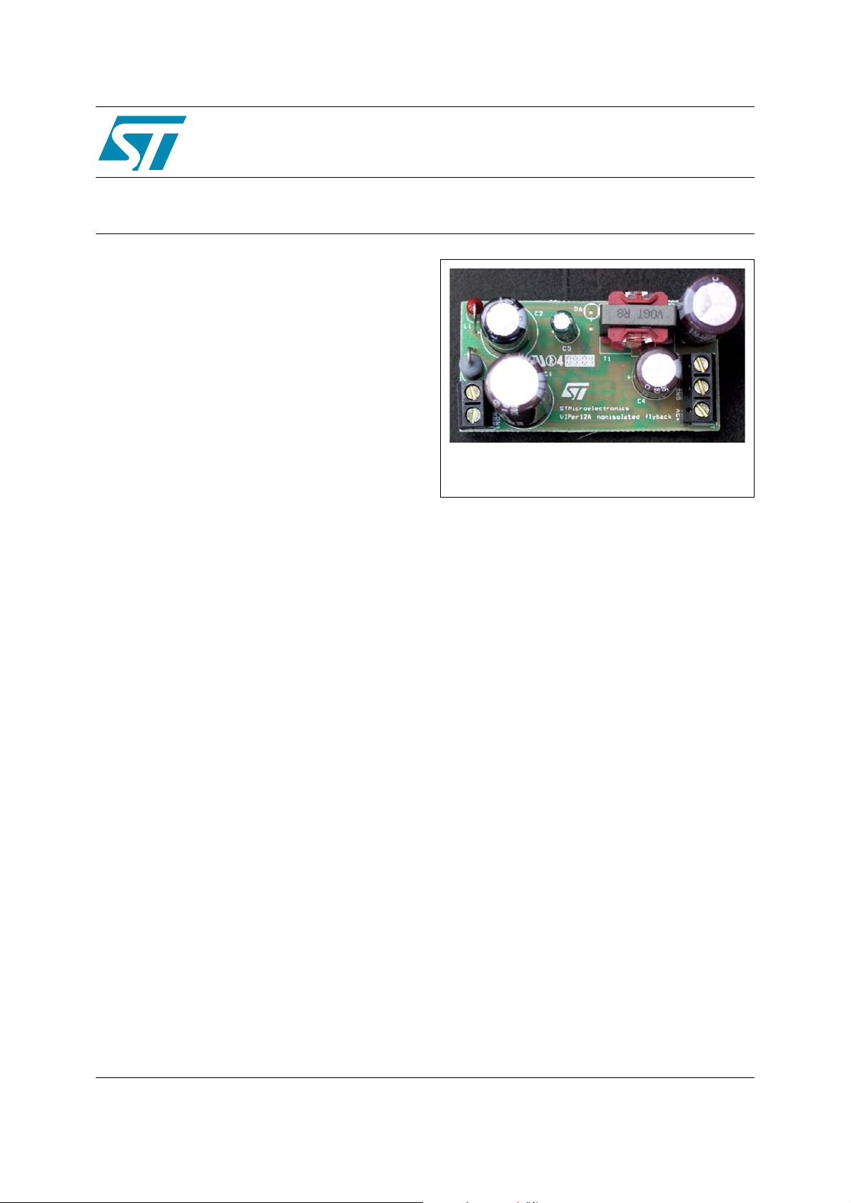
STEVAL-ISA006V1
with VIPer12AS
Data Brief
This reference design is an auxiliary power supply
based on the VIPer12AS monolithic device and
can be used to produce multiple non isolated
positive or negative voltage outputs.
This solution is based on an offline discontinuous
current mode fly-back converter without isolation
between input and output. The fly-back topology
allows the exploitation of the VIPer12AS current
capability when compared with the buck converter
based power supply. To ensure power supply low
cost, the isolation between input and output is not
provided. This greatly simplifies the transformer
design and production. The VIPer12AS
incorporates the PWM controller with a 60kHz
internal oscillator and the vertical Power MOSFET
switch in a SO-8 package. The presented power
supply has four variants. All the variants have
been incorporated in the presented reference
board through different assembly options.
STEVAL-ISA006V1
ST Components
■ VIPer12AS off-line SMPS primary
■ STPR120A diode, fast recovery trr =25ns 200V
1A SMA
■ STPS1L40A diode, schottky, 40V 1A,
■ TS2431ILT programmable shunt voltage
reference
July 2007 Rev 1 1/5
For further information contact your local STMicroelectronics sales office
www.st.com
5
Page 2

General circuit description STEVAL-ISA006V1
1 General circuit description
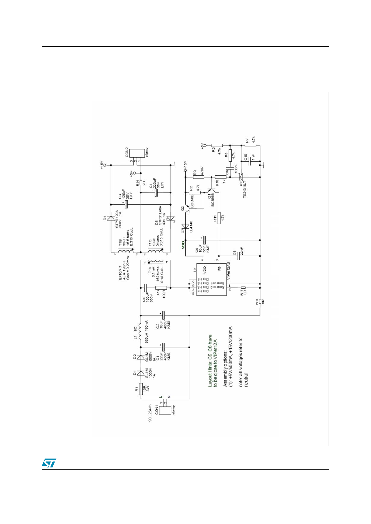
The output of the converter is not isolated from the input. For this reason the reference ground
is common for an input and output connection terminal. The input capacitor C1 is charged from
the mains by single rectification consisting of diodes D1 and D2. Two diodes in series are used
for EMI reasons to sustain burst pulses of 2kV. Capacitor C1 together with capacitor C2 and
inductor L1 form an EMI filter. The DC voltage at C2 is then applied to the transformer primary
winding through the internal Power MOSFET switch of VIPer12 during the switching period ON
time. The snubber circuit consisting of resistor R3 and capacitor C6 reduces the voltage spike
across the transformer primary winding due to the parasitic leakage inductance. Through
rectifiers D4 and D5 and through smoothing capacitors C3 and C4, the power supply provides
two outputs from two transformer windings. The VIPer12AS is supplied by a 15V output voltage
through transistor Q2 and diode D7. The voltage feedback loop senses the 5V output through
resistor divider R5, R7. The control IC U2 compares the resistor divider output voltage to the
internal reference voltage of 2.5V and changes the cathode voltage accordingly to keep 5V
output stable. The FB pin current will decrease the peak primary current to reduce the power
delivered to the outputs.
2/5
Page 3

STEVAL-ISA006V1 Board schematic
2 Board schematic
Figure 1. Scheme
3/5
Page 4

Revision history STEVAL-ISA006V1
3 Revision history
Table 1. Revision history
Date Revision Changes
20-Jul-2007 1 Initial release.
4/5
Page 5

STEVAL-ISA006V1
Please Read Carefully:
Information in this document is provided solely in connection with ST products. STMicroelectronics NV and its subsidiaries (“ST”) reserve the
right to make changes, corrections, modifications or improvements, to this document, and the products and services described herein at any
time, without notice.
All ST products are sold pursuant to ST’s terms and conditions of sale.
Purchasers are solely responsible for the choice, selection and use of the ST products and services described herein, and ST assumes no
liability whatsoever relating to the choice, selection or use of the ST products and services described herein.
No license, express or implied, by estoppel or otherwise, to any intellectual property rights is granted under this document. If any part of this
document refers to any third party products or services it shall not be deemed a license grant by ST for the use of such third party products
or services, or any intellectual property contained therein or considered as a warranty covering the use in any manner whatsoever of such
third party products or services or any intellectual property contained therein.
UNLESS OTHERWISE SET FORTH IN ST’S TERMS AND CONDITIONS OF SALE ST DISCLAIMS ANY EXPRESS OR IMPLIED
WARRANTY WITH RESPECT TO THE USE AND/OR SALE OF ST PRODUCTS INCLUDING WITHOUT LIMITATION IMPLIED
WARRANTIES OF MERCHANTABILITY, FITNESS FOR A PARTICULAR PURPOSE (AND THEIR EQUIVALENTS UNDER THE LAWS
OF ANY JURISDICTION), OR INFRINGEMENT OF ANY PATENT, COPYRIGHT OR OTHER INTELLECTUAL PROPERTY RIGHT.
UNLESS EXPRESSLY APPROVED IN WRITING BY AN AUTHORIZED ST REPRESENTATIVE, ST PRODUCTS ARE NOT
RECOMMENDED, AUTHORIZED OR WARRANTED FOR USE IN MILITARY, AIR CRAFT, SPACE, LIFE SAVING, OR LIFE SUSTAINING
APPLICATIONS, NOR IN PRODUCTS OR SYSTEMS WHERE FAILURE OR MALFUNCTION MAY RESULT IN PERSONAL INJURY,
DEATH, OR SEVERE PROPERTY OR ENVIRONMENTAL DAMAGE. ST PRODUCTS WHICH ARE NOT SPECIFIED AS "AUTOMOTIVE
GRADE" MAY ONLY BE USED IN AUTOMOTIVE APPLICATIONS AT USER’S OWN RISK.
Resale of ST products with provisions different from the statements and/or technical features set forth in this document shall immediately void
any warranty granted by ST for the ST product or service described herein and shall not create or extend in any manner whatsoever, any
liability of ST.
ST and the ST logo are trademarks or registered trademarks of ST in various countries.
Information in this document supersedes and replaces all information previously supplied.
The ST logo is a registered trademark of STMicroelectronics. All other names are the property of their respective owners.
© 2007 STMicroelectronics - All rights reserved
STMicroelectronics group of companies
Australia - Belgium - Brazil - Canada - China - Czech Republic - Finland - France - Germany - Hong Kong - India - Israel - Italy - Japan -
Malaysia - Malta - Morocco - Singapore - Spain - Sweden - Switzerland - United Kingdom - United States of America
www.st.com
5/5
 Loading...