

Page 1
1.8W buck topology power supply evaluation board
Features
■ Switch mode general purpose power supply
■ Input: 85 to 264Vac @ 50/60Hz
■ Output: 15V, 100mA @ 50/60Hz
■ Output power (pick): 1.6W
■ Second output through linear regulator: 5V / 60
or 20mA
Description
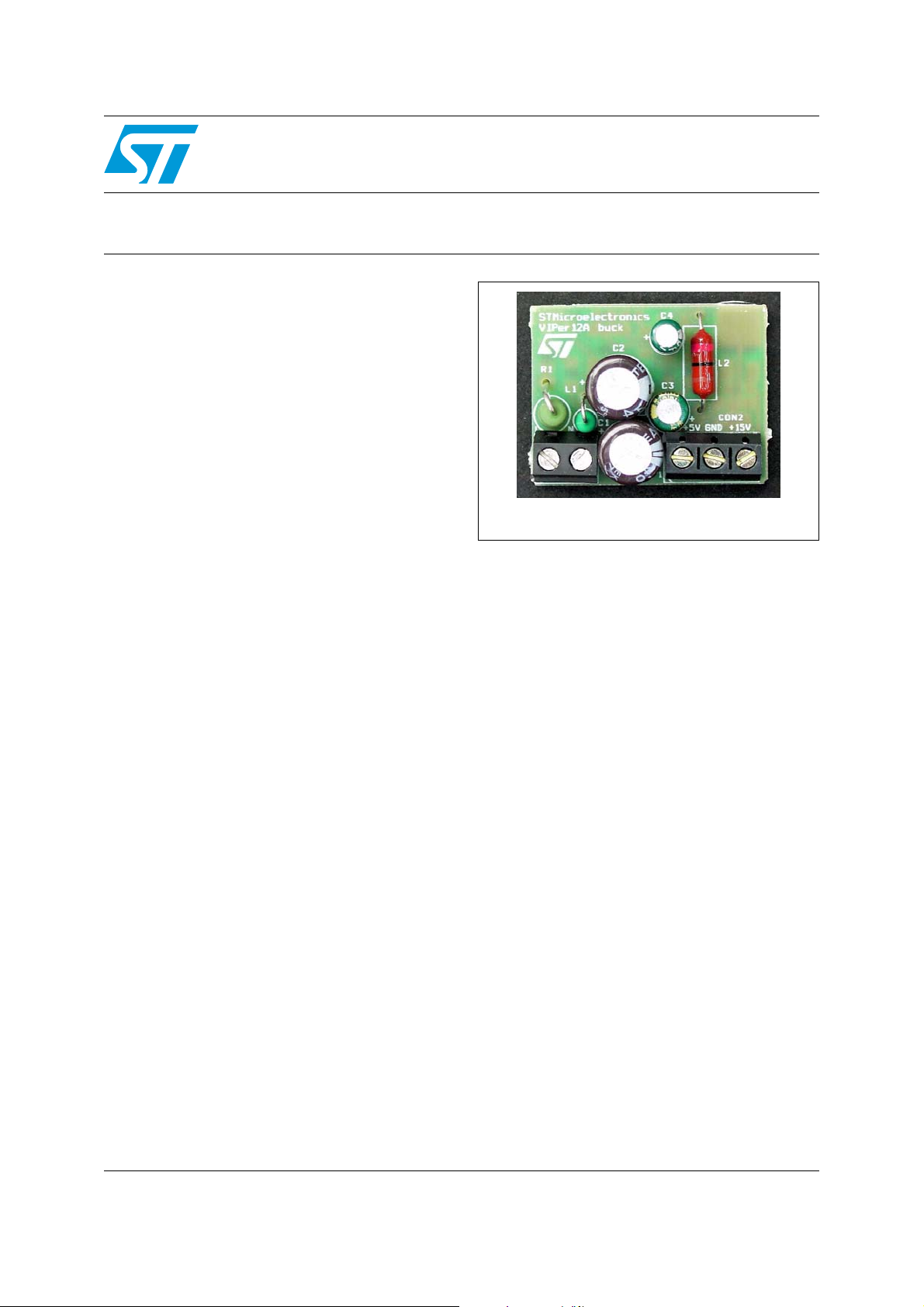
STEVAL-ISA005V1
with VIPer12AS
Data Brief
This evaluation board is an auxiliary power supply
based on the VIPer12AS monolithic device with
rather low output power required. It is a buck
(step-down) converter with a positive output
voltage referenced to the common ground based
on the monolithic device VIPer12AS, which is a
device that incorporates the PWM controller
together with the vertical Power MOSFET switch
in a SO-8 package.
STEVAL-ISA005V1
ST Components
■ VIPer12AS Off-line SMPS Primary
■ L78L05CD or L78M05CDT positive voltage
regulator for optional 5V second output
July 2007 Rev 1 1/5
For further information contact your local STMicroelectronics sales office.
www.st.com
5
Page 2

General circuit description STEVAL-ISA005V1
1 General circuit description
Input capacitor C1 is charged from line via a one way rectifier consisting of diodes D1 and
D2. Two diodes in series are used for EMI reasons to sustain burst pulses of 2kV.
Capacitor C1 together with capacitor C2 and inductor L1 forms an EMI filter. The DC voltage
at C2 is then applied to the VIPer12 that works as a high side switch. It means that the IC
and corresponding supply and feedback loop circuitry is floating. The IC supply circuit
consists of the high voltage diode D4, ceramic capacitor C7, low voltage diode D7 and
capacitor C4. The voltage feedback loop is provided via zener diode D3, resistor R3 and
capacitor C6. The diode D7 between capacitor C7 and C4 ensures proper start-up of the
converter.
Thanks to this diode the feedback loop circuit is separated from the supply circuit. The
VIPer12 internal start-up current source charges the IC supply capacitor C4 to a specified
start-up threshold voltage of about 16V. As soon as the voltage of C4 reaches the start-up
threshold, the internal 60kHz oscillator sets the internal flipflop and the internal highside
Power MOSFET is turned on through the output driver. The Power MOSFET applies the
bulk capacitor C1 and C2 high voltage to the power diode cathode and to one terminal of the
inductor. Since the voltage at the output capacitor C3 connected to the inductor's second
terminal is much lower than the input bulk capacitor voltage, inductor current will ramp-up.
As soon as the inductor current ramp reaches the VIPer's internal set-point defined by the
feedback loop, the internal power switch turns off. The inductor keeps the direction of the
current flowing and it reverses the voltage at C3. The inductor current then flows through the
forward biased D5 diode and charges output capacitor C3.
In this switch-off phase the VIPer12 source terminal sees a negative level of the forward
biased D5 (when referenced to ground) so it can be considered as grounded. This allows
the inductor current to flow also through D4, supply the VIPer12 and give the feedback
information concerning the output voltage. The converter output voltage at the 15V terminal
is determined by the voltage drop across zener diode D3 together with the voltage drop
across the resistor R3 and FB pin voltage. Resistor R3 limits the feedback current to a safe
value lower than the maximum rating specified in the datasheet. Capacitor C6 protects the
FB input against EMI. Regulator U2 accommodated in a DPAK or SO-8 package is optional
and can be assembled if the power supply for a microcontroller or logic part is required. The
DPAK package version of U2 is dedicated for 60mA output current option while the U3 in
SO-8 package provides a maximum output current of 20mA.
2/5
Page 3

STEVAL-ISA005V1 Board Schematic
2 Board Schematic
Figure 1. Scheme
3/5
Page 4

Revision history STEVAL-ISA005V1
3 Revision history
Table 1. Document revision history
Date Revision Changes
23-Jul-2007 1 Initial release.
4/5
Page 5

STEVAL-ISA005V1
Please Read Carefully:
Information in this document is provided solely in connection with ST products. STMicroelectronics NV and its subsidiaries (“ST”) reserve the
right to make changes, corrections, modifications or improvements, to this document, and the products and services described herein at any
time, without notice.
All ST products are sold pursuant to ST’s terms and conditions of sale.
Purchasers are solely responsible for the choice, selection and use of the ST products and services described herein, and ST assumes no
liability whatsoever relating to the choice, selection or use of the ST products and services described herein.
No license, express or implied, by estoppel or otherwise, to any intellectual property rights is granted under this document. If any part of this
document refers to any third party products or services it shall not be deemed a license grant by ST for the use of such third party products
or services, or any intellectual property contained therein or considered as a warranty covering the use in any manner whatsoever of such
third party products or services or any intellectual property contained therein.
UNLESS OTHERWISE SET FORTH IN ST’S TERMS AND CONDITIONS OF SALE ST DISCLAIMS ANY EXPRESS OR IMPLIED
WARRANTY WITH RESPECT TO THE USE AND/OR SALE OF ST PRODUCTS INCLUDING WITHOUT LIMITATION IMPLIED
WARRANTIES OF MERCHANTABILITY, FITNESS FOR A PARTICULAR PURPOSE (AND THEIR EQUIVALENTS UNDER THE LAWS
OF ANY JURISDICTION), OR INFRINGEMENT OF ANY PATENT, COPYRIGHT OR OTHER INTELLECTUAL PROPERTY RIGHT.
UNLESS EXPRESSLY APPROVED IN WRITING BY AN AUTHORIZED ST REPRESENTATIVE, ST PRODUCTS ARE NOT
RECOMMENDED, AUTHORIZED OR WARRANTED FOR USE IN MILITARY, AIR CRAFT, SPACE, LIFE SAVING, OR LIFE SUSTAINING
APPLICATIONS, NOR IN PRODUCTS OR SYSTEMS WHERE FAILURE OR MALFUNCTION MAY RESULT IN PERSONAL INJURY,
DEATH, OR SEVERE PROPERTY OR ENVIRONMENTAL DAMAGE. ST PRODUCTS WHICH ARE NOT SPECIFIED AS "AUTOMOTIVE
GRADE" MAY ONLY BE USED IN AUTOMOTIVE APPLICATIONS AT USER’S OWN RISK.
Resale of ST products with provisions different from the statements and/or technical features set forth in this document shall immediately void
any warranty granted by ST for the ST product or service described herein and shall not create or extend in any manner whatsoever, any
liability of ST.
ST and the ST logo are trademarks or registered trademarks of ST in various countries.
Information in this document supersedes and replaces all information previously supplied.
The ST logo is a registered trademark of STMicroelectronics. All other names are the property of their respective owners.
© 2007 STMicroelectronics - All rights reserved
STMicroelectronics group of companies
Australia - Belgium - Brazil - Canada - China - Czech Republic - Finland - France - Germany - Hong Kong - India - Israel - Italy - Japan -
Malaysia - Malta - Morocco - Singapore - Spain - Sweden - Switzerland - United Kingdom - United States of America
www.st.com
5/5
 Loading...