

Page 1
Mono-phase / multi-tariff energy meter
based on the ST72321BR9 and STPM14
Features
■ Cost-effective and flexible
■ Meets Class 1 accuracy for I
I
= 80 A according to IEC 61036:1996 + A1:
max
2000 - Static meter for active energy (classes 1
and 2)
■ Operating voltage range 220 V ± 20%
■ Continuously detects and displays no-load
conditions, reverse direction, fraud and case
tamper conditions
■ Configurable number of tariffs (1 to 4) and
maximum demand type (day, one month or
three month)
■ Accumulated data for whole meter life
(total kWh consumption, average MD
(maximum demand), total number of tariffs,
tariff time slots, consumption under different
tariff rates, power failure date/time)
■ Data for last 12 months (consumption under
tamper mode for each month, first/last
case/fraud tamper date/time, total tamper time
and power failure accumulating time for each
month)
■ Data for absolute maximum demand (absolute
MD, date/time) according to type of MD
requested
■ SW LCD driver for 24 x 4 segment LCD glass
with contrast control
■ RTC with SPI for real date/time
■ EEPROM with SPI for storing 256 Kb of data
■ Case tamper detection even in power-down
■ External switch for viewing all data stored in
EEPROM sequentially even when AC power is
not available
■ Battery backup to detect tampering and see all
parameters stored in EEPROM even during
power-down
= 5 A and
B
STEVAL-IPE009V1
Data Brief
STEVAL-IPE009V1
■ Single point and fast calibration of the STPM14
for Class 1 meter.
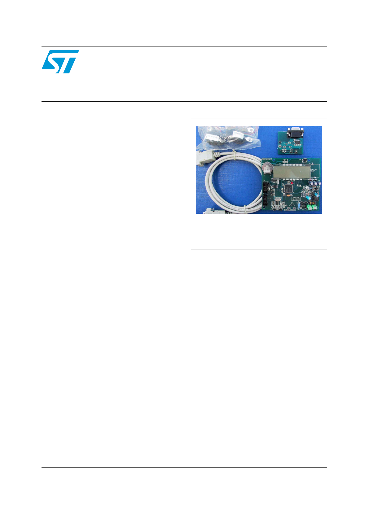
Description
This demonstration board is an integrated system
designed to provide the user with a complete,
ready-to-use energy meter application. It is a
medium-end solution for power metering, using
the ST72F321BR9T6 microcontroller, the
M41T94 RTC (real-time clock), the M95256
EEPROM and the STPM14 energy meter ASSP
device.
The multi-tariff energy meter demonstration board
implements many features that can be used as a
starting platform for evaluation and development
of meter applications, including multi-tariff
management, absolute and average maximum
demand calculation, two types of tamper
management, and power failure management.
September 2008 Rev 1 1/7
For further information contact your local STMicroelectronics sales office.
www.st.com
7
Page 2
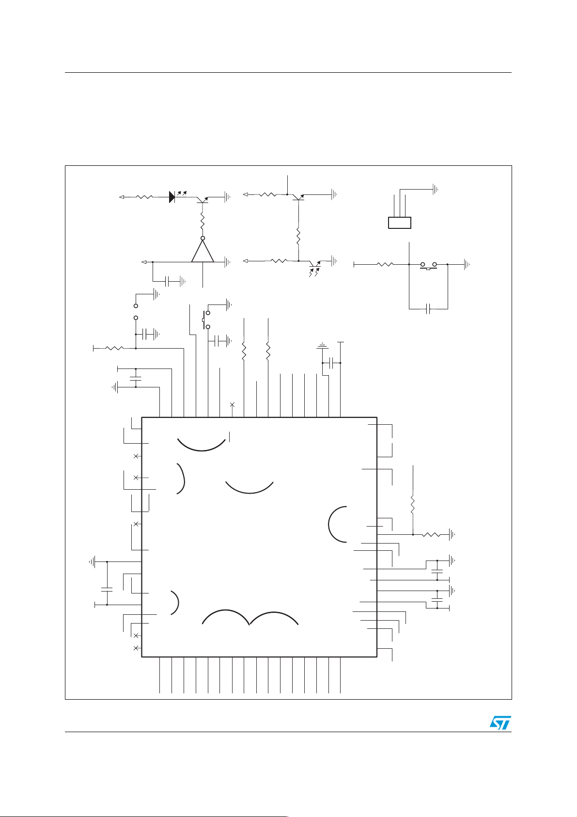
Schematic diagram STEVAL-IPE009V1
1 Schematic diagram
1.1 Multi-tariff single-phase meter
Figure 1. Schematic - microcontroller and IrDA section, MCU oscillator/reset
IrDA section
+5.0 VB
C5
+5.0 VB
+5.0 V
10 kΩ
R38
+5.0 VB
100 nF
OSC2
IROUT
PA5
PP
V
U6
JP1
C12
1 2
PA4RESET
IRQSTPM
OSC1
IRIN
Ω
D10
R39
39
1
+5.0 V
C33
C13
10 nF
100 nF
47
48
49
PA4
SS_1
V
50
PA5
51
52
PA6/SDAI
PA7/S CLI
53
/ICCSEL
PP
V
54
RESET
EVD
55
TLI
56
SS_2
57
V
58
OSC2
59
OSC1
DD_2
60
V
61
PE0/T DO
62
PE1/RDI
PE2
63
PE41PE52PE63PE74PWM3/PB05PWM2/PB16PWM1/PB27PWM0/PB38ARTCLK/PB4
PE3
64
100 nF
46
DD_1
V
U7A
PA3
3
TMPD
45
C
2
I
SCI
Q3
2
R30
1 2147
IROUT
SW1
PA2
BC847
1
Ω
3 k
C14
IRQRTC
IRQBUTT
43
44
PA0
PA1
ei0
74HC04
10 nF
42
SS/PC7
ei2
R41
+5.0 V+5.0 V
SDO
SCL
R7
R5
0 Ω
SDI
ICCCLK
ICCDATA
40
39
41
PC5/MOSI/AIN14
PC6/SCK/ICCCLK
PC4/MISO/ICCDATA
SPI
SPI
ST72F321BR9T6
ARTIC1/PB510ARTIC2/PB611PB712AIN0/PD013AIN1/PD114AIN2/PD215AIN3/PD3
9
Ω
IRIN
10 k
321
R40
220
Ω
R29
10 K
0 Ω
COM1
COM2
37
38
PC3/ICAP1_B
ei3
Q2
BC847
Q1
PHOTO NPN
1
2
COM3
COM4
35
36
34
PC2/ICAP2_B
PC0/OCMP2_B/AIN12
PC1/OCMP1_B/AIN13
ei1
MCU oscillator/reset
+5.0 VB
+5.0 VB
C19
100 nF
33
SS_0
DD_0
V
V
ICAP2_A/AIN11/PF5
BEEP/PF1
V
MCO/AIN8/PF0
V
AIN7/PD7
AIN6/PD6
16
EXTCLK_A/PF7
OCMP2_A/AIN9/PF3
SS_3
DD_3
V
AREF
AIN5/PD5
ICAP1_A/PF6
OCMP1_A /AIN10/PF4
PF2
SSSA
V
AIN4/PD4
R35
AM00281
OSC1
OSC2
123
X1
32
31
30
29
28
27
26
25
21 22 23 24
20
19
18
17
Ω
4.7 K
PF6
PF5 PF7
PF4
NLCD
PD5
PD4
NPD
PD6
RESET
PFD
R1
PD7
16 MHz
10 kΩ
R2
C31
SW2
10 nF
10 kΩ
C25
C24
100 nF
+5.0 VB
+5.0 VB
100 nF
Microcontrollers section
NERTC
EMEM
PE6
PE7
PB0
PB1
PB2
PB3
PB4
PB5
PB6
2/7
PB7
PD0
PD1
PD2
PD3
Page 3
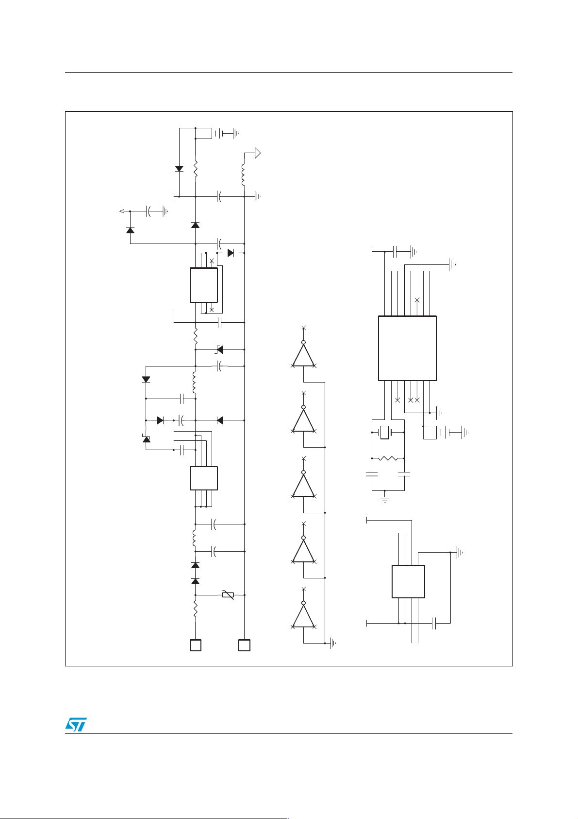
STEVAL-IPE009V1 Schematic diagram
Figure 2. Schematic - power management, RTC/memory SPI block
2
R4 5 KΩ
D4 BAT49
+5.0 VB
C1
100 µF
+
+
+5.0 V
PFD
C3
LL4148
D13
1
OUT
V
U2
L78L05AC
IN
V
8
7
0.25 W
R3
22E
C4
25 V
100 nF
50 V
10 µF
C2
S1S
22 nF 25 V
U1
8
L1 BC1
470 µH 100 MA
D6
D5
RF1
PHASE
1
J1
D12
1N4148
600 V
1 A
D2
STTH1L06
D3
DZ1
9.1 VZ
Power management section
3
GND2GND
L11 MH
250 mA
3
2
FB
1000 V
1000 V
10R 1 Ω
3
BT1
C11
+
+
1N4148
C10
+
+
4
NC
GND6GND
NC
5
D8
4
DD
V
D5D6D7D
C7
1 µF
C7
C6
1 µF
C6
1 A
1 A
CON1
1
4.8 V
L2 1 µH 150 mA
100 µF
100 µF 25 V
D11
1N4148
25 V
C9
100 nF
DZ2
10 VZ
C8
47 µF
25 V
600 V
1 A
STTH1L06
VIPER12ADIP
450 V
450 V
275 V 8.6 J
RV1
J2
F
1
Mains 230 VAC
CON1
U7F
14
U7E
14
U7D
U7C
U7B
Not used
13 12
11 10
9 8147
5 6147
3 4147
7
7
74HC04
74HC04
Y2
74HC04
74HC04
74HC04
C28
RTC/memory SPI block
+5.0 VB
U5
32.768 KHz
+5.0 VB +5.0 VB
C30+
100 nF
NERTC
IRQRTC
SDI
16
12
11
15
14
13
CC
NE
SDI
V
THS
SQW
NIRQ/FT/OUT
XI1XO2NRST3WDI4NRSTIN15NRSTIN26VBAT7V
R37
1 MΩ
C29
15 pF
SDO
EMEM
3
2
1
4
S
Q
W
V
CC
U4
D5C6HOLD7V
8
SDI
SCL
SCL
SDO
9
10
SCL
8
15 pF
SS
SDO
SS
2
3
M95256
C27
100 nF
AM00282
M41T94
1
BT2
BATTERY 3 V
3/7
Page 4

Schematic diagram STEVAL-IPE009V1
Figure 3. Schematic - measurement section, LCD block, ICC/STPM01 connectors
AM00283
15 pF
C22
4.194304
Ilp211Iln2
STPM14
MHz
R11
R14 2 MΩ
2,21
R121 MΩ
C21
KΩ
15 pF
R19
150 KΩ
R18 2 MΩ
Y1
NPD
SCS
TMPD
NLCD
15
4
17
Syn
CLKout
DDD
SS
V
5
12
16
14
13
IN
Vip
V
CLKin
CC
DDA
OTP
V
V
V
Ilp19Iln1
6
8
7
10
3
18
19
Scl
Scs
Sda
U3
D9
1 2
750 Ω
R6
IRQSTPM
C18
LED20MON1MOP2V
MON
1 µF
C26
TP1
LED
IRQSTPM
33 nF
R23
R22
R21
R24 470 Ω
200 KΩ
270 KΩ 270 KΩ
TP2
MON
MON
F
+5.0 VB
PP
V
RESET
R36
10 KΩ
JA1
J6
PA4
PA5
12345678910111213
J7
28
OSC1
10
123456789
TMPD
NLCD
VOTP
SCS
PD5
PF6
PD7
PF5
PF7
ICCCL K
NPD
+5.0 V
PD3PD2
PD1
ICCDATA
123456789
10
PB5
PB3PB2
PB7
192021222324252627
18
C32
100 nF
ICP connector
PE7
PB1
14
151617
LCD DE7936/V
+5.0 V
C17
1 µF
C16
1 µF
C15
1 nF
F
Measurement section
VOTP
C20
R8 1 KΩ
4.4
2
J4
10 nF
R13 1 KΩ
R15 1 KΩ
F
R10
4.4 1%
R9
1%
1
Current transformer
J5
C23
4.4 1%
4.4
1%
1
2
10 nF
R20 1 KΩ
R17
R16
F
phase
phase
Mains
Current transformer
230 VAC
COM4
COM2
COM3
LCD block ICC/STPM01 connectors
56 KΩ
R34
56 KΩ
R25
PF4
COM1
56 KΩ
R33
56 KΩ
R28
PD6
56 KΩ
R32
56 KΩ
R27
PD4
PD0
56 KΩ
R31
56 KΩ
R26
+5.0 VB
PB6
COM2
COM3
COM4 COM1
PB4
PB0
PE6
4/7
Page 5

STEVAL-IPE009V1 Schematic diagram
1.2 SCI-interface
Figure 4. Schematic - SCI-interface
J2
CON2
1
2
2
1
100 nF
C4
100 nF
50 V
R4
10 KΩ
R2
220 Ω
Q2
PHOTO NPN
C3
50 V
100 nF
50 V
C5
100 nF
50 V
+5.0V
C2
U1
1
+
C1
2
V+
3
C1–
4
C2+
5
C2–
6
V–
7
T2OUT
8
R2IN
ST232C
+5.0 V+5.0 V
R5
10 kΩ
IRIN
3
2
Q3
BC847
1
V
DD
GND
T1OUT
R1IN
R1OUT
T1IN
T2IN
R2OUT
16
15
14
13
12
11
10
9
C1
100 nF
50 V
IROUT
1
6
2
7
3
8
4
9
5
R1 3 kΩ
P1
RS232
2
+5.0 V
2
D1
1
3
1
IROUT
IRIN
R3
39 Ω
LN01201CAL(U)
Q1
BC847
2
1
CON2
J1
)
AM00284
5/7
Page 6

Revision history STEVAL-IPE009V1
2 Revision history
Table 1. Document revision history
Date Revision Changes
22-Sep-2008 1 Initial release.
6/7
Page 7

STEVAL-IPE009V1
Please Read Carefully:
Information in this document is provided solely in connection with ST products. STMicroelectronics NV and its subsidiaries (“ST”) reserve the
right to make changes, corrections, modifications or improvements, to this document, and the products and services described herein at any
time, without notice.
All ST products are sold pursuant to ST’s terms and conditions of sale.
Purchasers are solely responsible for the choice, selection and use of the ST products and services described herein, and ST assumes no
liability whatsoever relating to the choice, selection or use of the ST products and services described herein.
No license, express or implied, by estoppel or otherwise, to any intellectual property rights is granted under this document. If any part of this
document refers to any third party products or services it shall not be deemed a license grant by ST for the use of such third party products
or services, or any intellectual property contained therein or considered as a warranty covering the use in any manner whatsoever of such
third party products or services or any intellectual property contained therein.
UNLESS OTHERWISE SET FORTH IN ST’S TERMS AND CONDITIONS OF SALE ST DISCLAIMS ANY EXPRESS OR IMPLIED
WARRANTY WITH RESPECT TO THE USE AND/OR SALE OF ST PRODUCTS INCLUDING WITHOUT LIMITATION IMPLIED
WARRANTIES OF MERCHANTABILITY, FITNESS FOR A PARTICULAR PURPOSE (AND THEIR EQUIVALENTS UNDER THE LAWS
OF ANY JURISDICTION), OR INFRINGEMENT OF ANY PATENT, COPYRIGHT OR OTHER INTELLECTUAL PROPERTY RIGHT.
UNLESS EXPRESSLY APPROVED IN WRITING BY AN AUTHORIZED ST REPRESENTATIVE, ST PRODUCTS ARE NOT
RECOMMENDED, AUTHORIZED OR WARRANTED FOR USE IN MILITARY, AIR CRAFT, SPACE, LIFE SAVING, OR LIFE SUSTAINING
APPLICATIONS, NOR IN PRODUCTS OR SYSTEMS WHERE FAILURE OR MALFUNCTION MAY RESULT IN PERSONAL INJURY,
DEATH, OR SEVERE PROPERTY OR ENVIRONMENTAL DAMAGE. ST PRODUCTS WHICH ARE NOT SPECIFIED AS "AUTOMOTIVE
GRADE" MAY ONLY BE USED IN AUTOMOTIVE APPLICATIONS AT USER’S OWN RISK.
Resale of ST products with provisions different from the statements and/or technical features set forth in this document shall immediately void
any warranty granted by ST for the ST product or service described herein and shall not create or extend in any manner whatsoever, any
liability of ST.
ST and the ST logo are trademarks or registered trademarks of ST in various countries.
Information in this document supersedes and replaces all information previously supplied.
The ST logo is a registered trademark of STMicroelectronics. All other names are the property of their respective owners.
© 2008 STMicroelectronics - All rights reserved
STMicroelectronics group of companies
Australia - Belgium - Brazil - Canada - China - Czech Republic - Finland - France - Germany - Hong Kong - India - Israel - Italy - Japan -
Malaysia - Malta - Morocco - Singapore - Spain - Sweden - Switzerland - United Kingdom - United States of America
www.st.com
7/7
 Loading...