

80 W offline PFC and LED driver demonstration board
Features
■ 80 W LED driver
■ 350 mA, 700 mA and 1 A LED current settings
■ High efficiency (~90%)
■ Wide input voltage range: 88 V to 265 VAC
■ High power factor: 0.982 for 230 V/50 Hz AC
■ Universal PWM input for dimming (external
board required)
■ Non-isolated SMPS
■ Brightness regulation between 0 and 100%
■ EMI filter implemented
■ EN55015 and EN61000-3-2 compliant
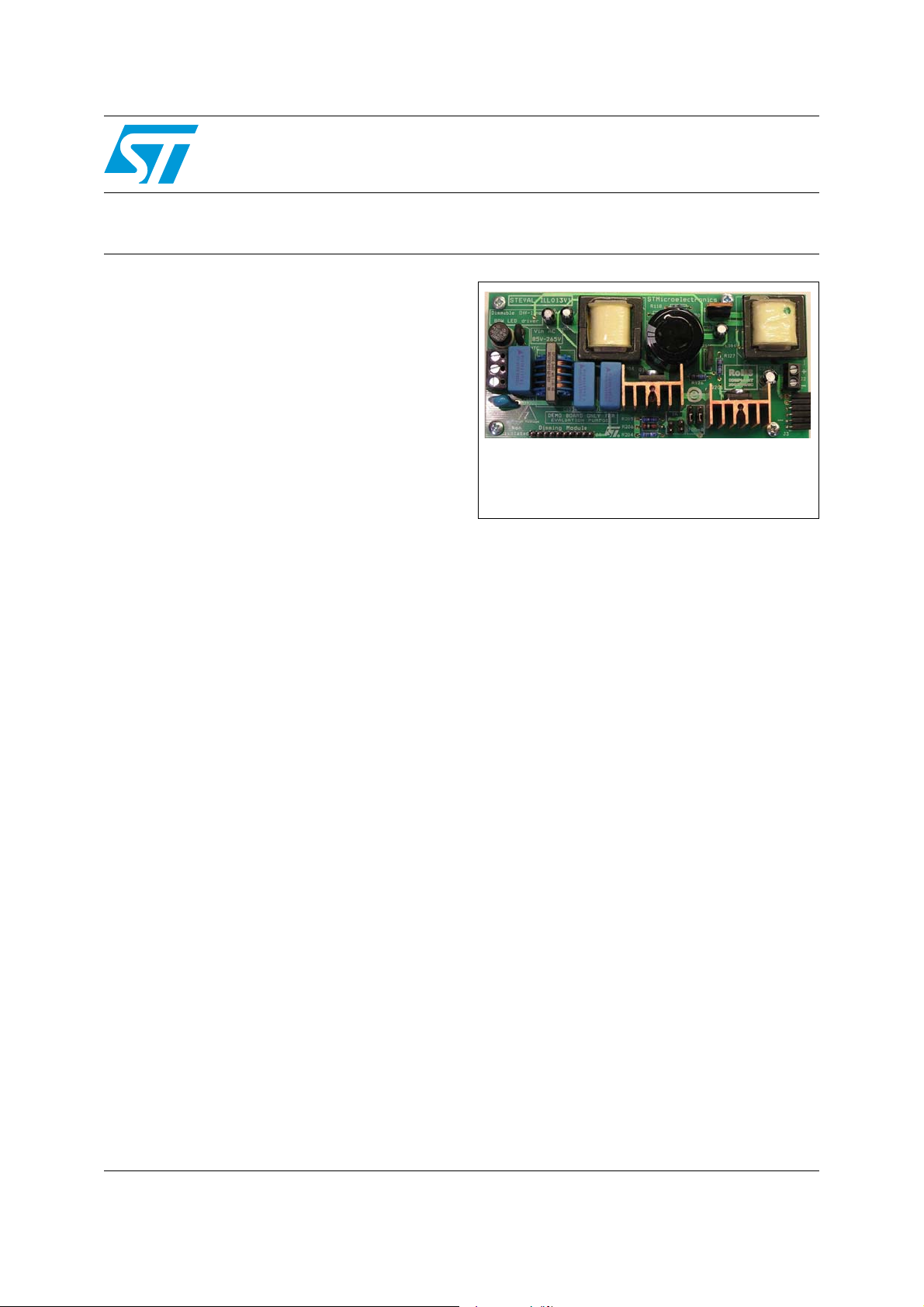
Description
STEVAL-ILL013V1
with dimming based on the L6562A
Data Brief
STEVAL-ILL013V1
This demonstration board design is complaint
with standard EN61000-3-2 (limits for harmonic
current emissions).
The use of high power LEDs in lighting
applications is becoming increasingly popular due
to rapid improvements in lighting efficiency, longer
life, higher reliability and overall cost
effectiveness. Dimming funtions are more easily
implemented in LEDs, and they are more robust
and offer wider design flexibility compared to
other light sources.
The STEVAL-ILL013V1 demonstration board is
an 80 W offline dimmable LED driver with high
power factor (PF) intended for 350 mA, 700 mA
and 1 A LEDs.
The converter is designed as a constant current
source to achieve the best lighting performance
from the LEDs, and can be used for lighting
applications from low power, low voltage to high
power, high voltage. This allows designers to
cover a wide range of different LED systems
using a single topology.
Additionally, in lighting applications where the
input active power is higher than 25 W and a high
power factor is required, the high PF converter
can be connected as the first stage, before the
modified BUCK converter.
March 2009 Rev 1 1/5
For further information contact your local STMicroelectronics sales office.
www.st.com
5

Circuit schematic STEVAL-ILL013V1
400V
16
16V
400V
PWM dimming signal
C112
150nF
C112
150nF
C103
220nF/X
C103
220nF/X
R122
R122
R120
15k
R120
15k
C206
1n5/63V
C206
1n5/63V
JP
JU
PER
JP
JU
PER
R111
R111
R115
33R
R115
33R
10
J4
J1
C208
0,47uF/450
C208
0,47uF/450
C110
33uF/35V
C110
33uF/35V
R121
82k
R121
82k
TR
CM
C
2x
22m
H/
1A
TR
CM
C
2x
22m
H/
1A
R207
1K
R207
1K
R109
47R
R109
47R
R102
1M
R102
1M
R101
1M
R101
1M
R106
270k
R106
270k
D202STST
PSC806D
D202STST
PSC806D
C109
12nF
C109
12nF
Q102BUBU
X8
Q102BUBU
X8
C113
47u/450V
C113
47u/450V
D101
18V/0.5
D101
18V/0.5
C207
330pF
C207
330pF
R1131R1R
R1131R1R
D104
1N
4148
D104
1N
4148
R114
1R
R114
1R
D103
TTH
1L06
D103
TTH
1L06
R204
1R
5/0.6W
R204
1R
5/0.6W
JP
JU
PER
JP
JU
PER
R208
47K
R208
47K
R107
270k
R107
270k
C204
390pF/63V
C204
390pF/63V
IN
GD
MP
VC
MU
LT
CS
U101
L6562A
U101
L6562A
IN
GD
CO
MP
ZC
VC
MU
LT
GN
CS
U201
L6562A
U201
L6562A
L20
1,6m
H /
172
Tu
rn
L20
1,6m
H /
172
Tu
rn
C108
12nF
C108
12nF
R206
2R
2/0.6W
R206
2R
2/0.6W
C102
470nF/X
C102
470nF/X
C111
2200nF
C111
2200nF
C205
820pF/63V
C205
820pF/63V
R105
15k
R105
15k
R126
20
R126
20
R116
47k
R116
47k
C2
01
22uF/35V
C2
01
22uF/35V
R108
47R
R108
47R
C106
100nF
C106
100nF
JP
JU
PER
JP
JU
PER
NT
10RNTNT
10R
R1121R1R
R1121R1R
101
101
R127
20
R127
20
C202
100nF
C202
100nF
R209
3.9K
R209
3.9K
C104
220nF/X
C104
220nF/X
R1
23
330
R1
23
330
R2
05
2R
7/0.6W
R2
05
2R
7/0.6W
R1
28
43k
R1
28
43k
F1
2A/250V
F1
2A/250V
J3
R119
1M
R119
1M
J2
C107
10uF/35V
C107
10uF/35V
R2033K3K
R2033K3K
Heatsink
Q2
01
ST
F9NM50N
Heatsink
Q2
01
ST
F9NM50N
R201
33R
R201
33R
D2011N1N
4148
D2011N1N
4148
D2041N1N
4148
D2041N1N
4148
C101
1n/
Y1
/ 250V ac
C101
1n/
Y1
/ 250V ac
R118
1M
R118
1M
BR
1A/250V
BR
1A/250V
D102
1N
4148
D102
1N
4148
R2021K1K
R2021K1K
R1
24
330
R1
24
330
Heatsink
Q101
ST
P8NM
50F
Heatsink
Q101
ST
P8NM
50F
R1
25
330
R1
25
330
R103
1M
R103
1M
JP
JU
PER
JP
JU
PER
R117
22k
R117
22k
D203
TTH
1L06A
D203
TTH
1L06A
R104
1M
R104
1M
C105
10nF
C105
10nF
R110
47k
R110
47k
C203
220pF/63V
C203
220pF/63V
1 Circuit schematic
Figure 1. Schematic diagram
+
-
J2J2J2
2
1
3
C113
C113
R117
R117
2200nF
2200nF
2
5
L6562A
L6562A
D104
D104
4
3
25
25
R1
R1
47u/450V
47u/450V
Q101
Q101
1
V
IN
C
VC
8
4148
4148
1N
1N
2
2
220nF/X
220nF/X
-
-
Q102
Q102
k
k
330
330
P
P
50F
50F
P8NM
P8NM
ST
ST
1
2
R115
R115
7
GD
COCOMP
ZCZCD
LT
MU
3
1
1A/250V
1A/250V
3
X8
X8
R121
R121
R120
R120
Heatsink
Heatsink
4 3
R116
R116
33R
33R
CS
GNGND
C105
C105
C110
C110
100nF
100nF
R105
R105
C101
C101
28
28
R1
R1
15k
15k
47k
47k
R111
R111
4
6
D101
D101
15k
15k
C106
C106
43k
43k
82k
82k
R114
R114
W
W
18V/0.5
18V/0.5
10nF
10nF
/ 250V ac
/ 250V ac
Y1
Y1
1n/
1n/
R113
R113
0
0
C107
C107
R112
R112
33uF/35V
33uF/35V
V
V
C208
C208
0,47uF/450
0,47uF/450
D202
D202
400V
1R
1R
16V
10uF/35V
10uF/35V
100nF
100nF
C202
C202
01
01
C2
C2
22uF/35V
22uF/35V
k
k
k
k
20
20
20
k
k
330
330
1M
1M
5
378
2
R109
R109
C109
C109
270k
270k
1M
1M
2
2
220nF/X
220nF/X
C102
C102
J1J1J1
R119
R119
150nF
150nF
C112
C112
R122
R122
47R
47R
D102
D102
1
1
BR
BR
2
2
2
470nF/X
470nF/X
321
24
24
R1
R1
R110
R110
4148
4148
1N
1N
R107
R107
R102
R102
R127
R127
1M
1M
0
0
1M
1M
+
+
k
k
330
330
22k
22k
C111
C111
47k
47k
270k
270k
C104
C104
20
U101
U101
R104
R104
R126
R126
V
400V
16
23
23
R1
R1
R118
R118
1L06
1L06
D103
D103
STTH
2/5
R101
R101
STTH
T101
T101
6
9
10101
R108
47R
R108
47R
12nF
12nF
12nF
12nF
C108
C108
R106
R106
R103
R103
1A
1A
H/
H/
22m
22m
C103
C103
2x
2x
C
C
34
1
1
CM
CM
TR
TR
12
1M
1M
1M
1M
C
C
NT
10R
10R
F1
F1
2A/250V
2A/250V
PSC806D
PSC806D
+
J3J3J3
s
s
rn
rn
Tu
Tu
172
172
H /
H /
1
1
1,6m
1,6m
L20
L20
01
01
Q2
Q2
U201
L6562A
U201
L6562A
R208
47K
R208
47K
-
21345
6
1L06A
1L06A
D203
D203
STTH
STTH
F9NM50N
F9NM50N
ST
ST
1
Heatsink
Heatsink
4 3
2
R201
33R
R201
33R
4148
4148
R202
R202
D201
D201
C203
C203
7
8
C
VC
V
IN
1
5
6
D
D
GD
ZC
GN
R207
R207
LT
MP
CO
MU
CS
2
3
4
R209
3.9K
R209
3.9K
4148
4148
D204
D204
213456789
10
J4J4J4
PWM dimming signal
12
12
12
220pF/63V
220pF/63V
1K
1K
R206
R206
2/0.6W
2/0.6W
2R
2R
MPER
MPER
2
2
JP
JP
4
4
JP
JP
JU
JU
1 2
3
3
JP
JP
1
1
JP
JP
C207
C207
MPER
MPER
JU
JU
MPER
MPER
JU
JU
MPER
MPER
JU
JU
05
05
R2
R2
7/0.6W
7/0.6W
2R
2R
R204
R204
5/0.6W
5/0.6W
1R
1R
C206
1n5/63V
C206
1n5/63V
C205
820pF/63V
C205
820pF/63V
C204
390pF/63V
C204
390pF/63V
9
9
R203
R203
330pF
330pF

STEVAL-ILL013V1 Circuit schematic
Table 1. Jumpers settings
I_LED JP1 JP2 JP3 JP4
350 mA0000
700 mA1100
1 A 0 0 1 1
3/5

Revision history STEVAL-ILL013V1
2 Revision history
Table 2. Document revision history
Date Revision Changes
06-Mar-2009 1 Initial release.
4/5

STEVAL-ILL013V1
Please Read Carefully:
Information in this document is provided solely in connection with ST products. STMicroelectronics NV and its subsidiaries (“ST”) reserve the
right to make changes, corrections, modifications or improvements, to this document, and the products and services described herein at any
time, without notice.
All ST products are sold pursuant to ST’s terms and conditions of sale.
Purchasers are solely responsible for the choice, selection and use of the ST products and services described herein, and ST assumes no
liability whatsoever relating to the choice, selection or use of the ST products and services described herein.
No license, express or implied, by estoppel or otherwise, to any intellectual property rights is granted under this document. If any part of this
document refers to any third party products or services it shall not be deemed a license grant by ST for the use of such third party products
or services, or any intellectual property contained therein or considered as a warranty covering the use in any manner whatsoever of such
third party products or services or any intellectual property contained therein.
UNLESS OTHERWISE SET FORTH IN ST’S TERMS AND CONDITIONS OF SALE ST DISCLAIMS ANY EXPRESS OR IMPLIED
WARRANTY WITH RESPECT TO THE USE AND/OR SALE OF ST PRODUCTS INCLUDING WITHOUT LIMITATION IMPLIED
WARRANTIES OF MERCHANTABILITY, FITNESS FOR A PARTICULAR PURPOSE (AND THEIR EQUIVALENTS UNDER THE LAWS
OF ANY JURISDICTION), OR INFRINGEMENT OF ANY PATENT, COPYRIGHT OR OTHER INTELLECTUAL PROPERTY RIGHT.
UNLESS EXPRESSLY APPROVED IN WRITING BY AN AUTHORIZED ST REPRESENTATIVE, ST PRODUCTS ARE NOT
RECOMMENDED, AUTHORIZED OR WARRANTED FOR USE IN MILITARY, AIR CRAFT, SPACE, LIFE SAVING, OR LIFE SUSTAINING
APPLICATIONS, NOR IN PRODUCTS OR SYSTEMS WHERE FAILURE OR MALFUNCTION MAY RESULT IN PERSONAL INJURY,
DEATH, OR SEVERE PROPERTY OR ENVIRONMENTAL DAMAGE. ST PRODUCTS WHICH ARE NOT SPECIFIED AS "AUTOMOTIVE
GRADE" MAY ONLY BE USED IN AUTOMOTIVE APPLICATIONS AT USER’S OWN RISK.
Resale of ST products with provisions different from the statements and/or technical features set forth in this document shall immediately void
any warranty granted by ST for the ST product or service described herein and shall not create or extend in any manner whatsoever, any
liability of ST.
ST and the ST logo are trademarks or registered trademarks of ST in various countries.
Information in this document supersedes and replaces all information previously supplied.
The ST logo is a registered trademark of STMicroelectronics. All other names are the property of their respective owners.
© 2009 STMicroelectronics - All rights reserved
STMicroelectronics group of companies
Australia - Belgium - Brazil - Canada - China - Czech Republic - Finland - France - Germany - Hong Kong - India - Israel - Italy - Japan -
Malaysia - Malta - Morocco - Singapore - Spain - Sweden - Switzerland - United Kingdom - United States of America
www.st.com
5/5
 Loading...