High brightness 32-LED evaluation board without diagnostic
based on the STP16CP05 LED driver
Features
■ 32 LED matrix driven by STP16CP05
■ LED current regulation
■ Adjustable brightness
■ Animated text capability
■ Adjustable blinking speed; several blinking
modes
■ Input voltage ranges from 5 V to 35 V input
voltage range
■ DC-DC converter for high efficiency
Description
This evaluation board represents a cost effective
solution to drive an array of high brightness LEDs,
using the LED driver STP16CP05. This driver
provides the same constant current for each of its
output channels, thus there is no difference in
brightness and color between the LEDs.
STEVAL-ILL003V2
Data Brief
STEVAL-ILL003V2
November 2007 Rev 1 1/4
For further information contact your local STMicroelectronics sales office.
www.st.com
4

Board schematic STEVAL-ILL003V2
1 Board schematic
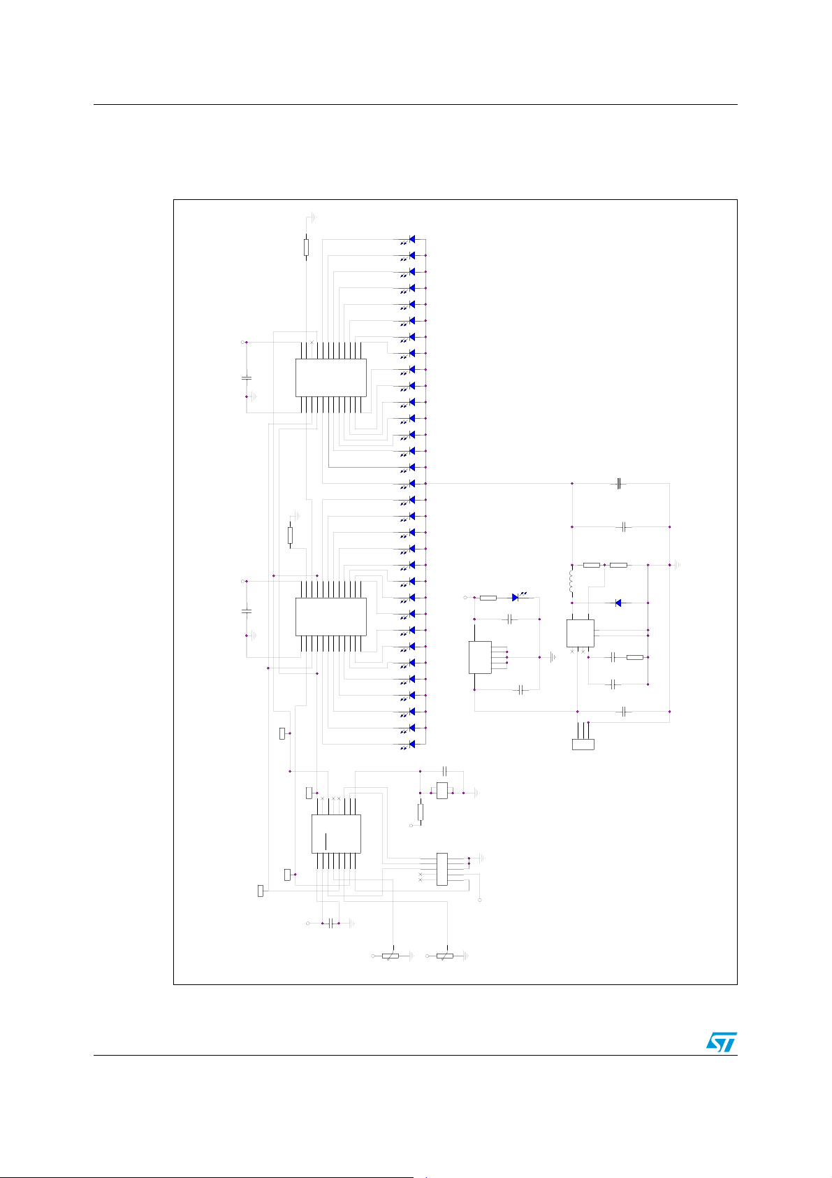
Figure 1. Schematic
1K2R21K2
R2
D32D32D16D16
D29D29 D31D31
D28D28D10D10
D27D27D13D13 D24D24
VCCVCC
C2
100nFC2100nF
23
24
22
Vdd
R-EXT
GND1SDI2CLK3/LE
STP16CPS05
STP16CPS05
20
21
/OE
SDO
OUT05OUT16OUT27OUT38OUT49OUT510OUT611OUT7
4
14
IO3
IO3
OUT813OUT9
OUT1015OUT1116OUT1217OUT1318OUT1419OUT15
12
D26D26
D25D25
D23D23D20D20D18D18
D22D22D2D2
D19D19
220uF/16V
220uF/16V
C11
C11
+
1
682
123
+
C10
C10
100uF/16V
100uF/16V
R5
6k8R56k8
R63kR6
3k
D34
D34
STPS340U
STPS340U
5
7
3
4
R7
4k7R74k7
C8
22nFC822nF
C7
220pFC7220pF
C9
10uF/35VC910uF/35V
D17D17
D15D15
1K2R11K2
R1
23
20
24
21
22
C1
100nFC1100nF
Vdd
R-EXT
GND1SDI2CLK3/LE
STP16CP05
STP16CP05
/OE
SDO
OUT05OUT16OUT27OUT38OUT49OUT510OUT611OUT7
4
14
OUT813OUT9
OUT1015OUT1116OUT1217OUT1318OUT1419OUT15
IO2
IO2
12
D14D14 D30D30
21
D33
GREEN LED
D33
R4
VCC
D9D9
1
Inhib
Gnd
Vout
Gnd
L78L33
L78L33
Gnd
D6D6 D11D11 D21D21
D5D5 D7D7 D12D12
Gnd
Vin
IO4
IO4
8
GREEN LED
560R4560
C6
100nFC6100nF
5
7
6
3
2
C5
L1 33uFL1 33uF
IO5 L5970DIO5 L5970D
100nFC5100nF
D4D4 D8D8
D3D3
J3J3
D1D1
C4
10nFC410nF
J5 CON3J5 CON3
J4J4
9
16
11
10
14
13
15
NC12NC
NC
PA7
PA0
PWM
IO1
IO1
Vss1Vdd2RESET3AIN04SCK5AIN26MOSI7CLKIN
ICCCLK
ICCDATA
8
VCC
ST7LITE09
ST7LITE09
J2J2
J1J1
VCC
C3
100nFC3100nF
VCC
3
12
P1
10KP110K
2/4
R3
1432
S1
10KR310K
VCC
12
SwitchS1Switch
ICCICC
1 2
3 4
5 6
7 8
9 10
VCC
3
P2
10KP210K
 Loading...