

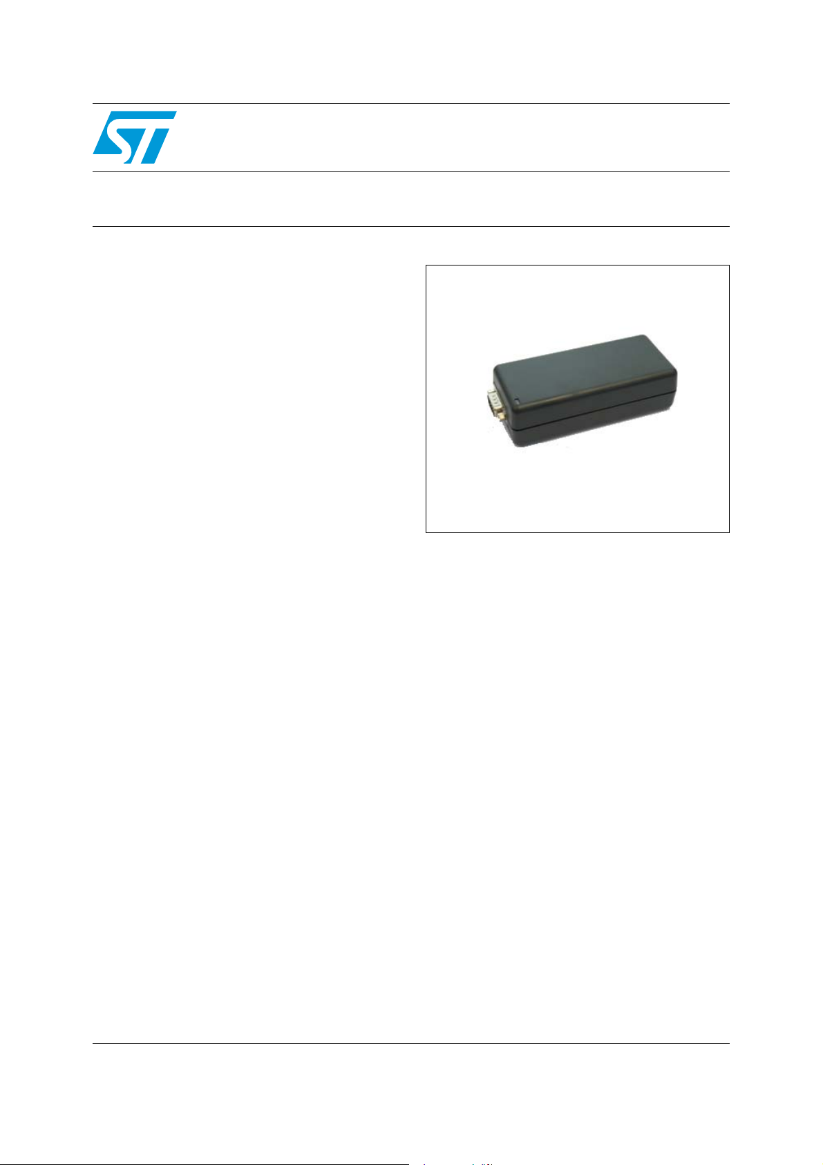
Remote-controlled PLM network module
based on the ST7540 and STM32F103C8
Features
■ PLM communication compliant with
EN50065-1 (band C)
■ FSK modulation with low frequency deviation
■ Centre frequency 132.5 kHz ± 0.2%
■ Bitrate: 2400 bits/s
■ Microcontroller for interfacing PLM with STB
■ Robust protocol implementation pursuant to
KNX protocol stack (EN50090)
■ Plug and play network formation
■ Logical network creation
■ Master-slave and peer-to-peer network
configuration
■ Node self-discovery to enable devices (nodes)
to discover other devices and/or to be
discovered by other devices
■ Node admission: automatic, using ID number
stored in each device
■ Network address management: selection,
announcements and conflict resolution
■ Operating temperature range: 0 °C -50 °C
■ RoHS compliant
Description
The STEVAL-IHP003V1 module is a PLM (power
line modem)-based demonstration application
intended as an evaluation platform for the ST7540
FSK power line transceiver and the
STM32F103C8 ARM-based 32-bit
microcontroller.
STEVAL-IHP003V1
Data brief
STEVAL-IHP003V1
the AC power line, by impressing a 132.5 kHz
carrier signal on the AC wiring system with
frequency shift keying modulation.
The module provides two ports, one dedicated to
the power line connection and the other to a
server connection.
On the top of the module housing, there is a twocolor LED to indicate the operating status of the
module.
In addition to the ST7540 power line transceiver
and STM32F103C8 microcontroller, the module
features an ST3232C for RS-232 interfacing and
a SPAC265-3W AC-DC switched-mode power
supply.
The module is dedicated to pay television
management, SmartPlug applications, home
appliance networks and various types of remotecontrolled power distribution.
For example, it can be used in hotels to act as an
interface between a set-top box in hotel rooms,
and a service server located at the hotel
reception. Communication is achieved through
April 2010 Doc ID 17440 Rev 1 1/4
For further information contact your local STMicroelectronics sales office.
www.st.com
4
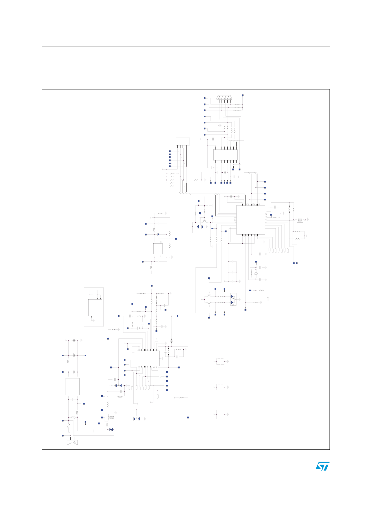
Schematic diagram STEVAL-IHP003V1
1 Schematic diagram
Figure 1. STEVAL-IHP003V1 circuit schematic
80TP80
P
R310R
R310R
T1OUT
C1-3C
TP69TP69
43TP43
P
T
00NF
00NF
1
1
F
F
µ
µ
0
0
1
1
NF
NF
0
0
0
0
1
1
F
F
µ
µ
0
0
1
1
NF
NF
0
0
F
F
µ
µ
0
0
1
1
384
A
_
N
R1_I
13
V
+3.3
R30
R30
V
3.3
+
R1IN
C2+4V-
0
0
7
7
P
P
T
T
TP40TP40
T
M.
M.
2
7
1
6
.
.
R35
R35
N
N
R34
N.M.
R34
N.M.
R33N.M.
R33N.M.
R36N.M.
R36N.M.
R31A 0R
R31A 0R
36A N.M.
36A N.M.
R
R
S
S
X
X
T
RT
R
CT
2
9
11
1
10
T
T
OU
T2IN
T1IN
2OU
1
R
R
N
I
2-
2
T2OUT
R
5
8
7
6
3
3
4TP74
7
7
7
P
P
T
T
TP
S
100NF
100NF
C22
C22
00NF
00NF
C271
C271
TP71TP71
TP72TP72
C20
C20
100NF
100NF
37
38
39
40
41
42
43
44
45
46
47
48
TP54TP54
K
K
1
1
F
F
N
N
C18
C18
0
0
10
10
F
5
5
2
2
C
100NFC
100N
38
38
C
C
1µF
1µF
EN
RE
G
3
1
D
RE
ED
ED
L
L
D6
D6
BI-
BI-
S
T
RT
C
TX
RX
TMS
4
3
35
36
_2
S
A13
PA1132PA1233PA1031P
S
V
VDD_2
PA14
PA15
PB3
PB4
PB5
PB6
PB7
BOOT0
PB8
-RTC
N
PB9
R
VSS_3
32_I
VDD_3
SC
TAMPE
O
13-
14C
PC
P
VBAT
PD0OSC_IN5PD1OSC_OUT6PC15-OSC_OUT4VSSA8VDDA9NRST
2
3
1
P45TP45
T
2
4
TP44TP4
53
TP53TP
2
TP52TP5
1
TP51TP5
0
0
5
5
P
P
T
T
5
8
26
2
29
30
2
8
3V
15
+3.
B13
B12
B
PA
PA9
P
PB1427P
P
VDD_1
VSS_1
PB11
PB10
PB2
PB1
PB0
PA7
U4
STM32F103C8T6U4STM32F103C8T6
PA6
PA5
PA4
PA3
A1
A2
PA0-WKUP
P
P
7
2
10
11
1
C26
C26
100NF
100NF
6
6
4
4
P
P
T
T
C33
22PF
C33
22PF
.
R32N.M.R32N.M
Y2
8MHzY28MHz
22PF
22PF
C32
C32
R28
N.M.
R28
N.M.
0K
0K
1
1
R23
R23
R37
R37
10K
10K
8
8
2
2
C
100NF
C
100NF
24
23
22
4
4
21
2
2
TP49TP49
10K
10K
R
R
20
19
18
17
16
15
14
13
TXD
RXD
CD/PDBUCLR/T
RX/TX
REG_DATA
TP47TP47
CLK_IN
AM07238v1
TP77TP77
J2
DB9-M ALEJ2DB9-M ALE
9
5
TP78TP78
TP79TP79
RAM
G
O
TP66TP66
PR
N
TP65TP65
.
_8
_8
N
N
.M
O
O
J3
J3
N
C
C
1
2345678
TP64TP64
TP63TP63
TP62TP62
TP61TP61
TP60TP60
TP59TP59
+3.3V
8
8
1
1
R
R
10K
10K
7
7
1
1
R
R
10K
10K
R16
R16
10K
10K
5
5
1
1
R
10K
R
10K
4
4
K
K
1
1
0
0
1
1
R
R
ST
R
CK
T
/
TMS
TDI
T
.
R27
N.M.R27
N.M
+3.3V
2µF
2µF
2
6
TP36TP3
TP35TP35
TP82TP82
10
10
2K 1%
2K 1%
8
8
R
t o F1
t o L3
769
10
1
1
0
0
69H14-21
69H14-21
T1Altern.
T1Altern.
1
5
27TP27
P
T
t o R4
1K1R51K1
6V
6V
F1
F1
C3
47µ
C3
47µ
+12V
C2
470µF16VC2470µF16V
TP8TP8
L2
L2
TP6TP6
3
PS1
SPAC265FC12A030
PS1
SPAC265FC12A030
2
2
P2TP
T
F1T-1A
F1T-1A
TP1TP1
1
TP7TP7
H
H
0µ
0µ
1
1
C1470µF16V
C1470µF16V
4
t
Vou
n
1
Vi
C39
C39
TP5TP5
33NFX2
33NFX2
H
L1
1mHL1
1m
0
0
0
0
3
3
K
K
4
7
7
P4TP
RV1
RV1
S0
S0
T
2
2
FX
FX
N
N
8
8
C4
6
C4
6
2
N2
N2
N
N
J1
CO
J1
CO
R5
4TP14
1
TP
TP13TP13
C6
10NFC610NF
5V_VDC
C5
2
TP12TP1
TP11TP11
0
0
P1
P1
T
T
9
TP9TP
6.8NFC56.8NF
µH
µH
0
0
2
2
2
2
L4
L4
R4
750RR4750R
1
4
T1
5
8
6
7-
22µHL322µH
T60403-K5024-X044T1T60403-K5024-X044
L3
D2
D2
M6T15CA
M6T15CA
S
S
R
5V_VDC
TP28TP28
TP29TP29
K
F
R8
68KR8
68
C7
10NFC7
10N
K
K
5
5
R31
R31
z
z
C12
C12
33PF
33PF
MH
MH
Y1
Y1
16
16
TP26TP26
5V_VDC
25
26
27
X_IN
TP25TP25
VDC
R
TEST228TEST1
7TP17
1
TP
7540
7540
5
TP15TP1
6
6
1
1
P
P
T
T
P18TP18
T
D4
BAT54SD4BAT54S
D
T
T
U1
S
U1
S
REG_DATA2Rx
CD_PD
GND3CL
4
1
D
D
/PD
TX
RX
RX/TX
CD
REG_DATA
C8
10µFC810µF
+12V
S
D3
BAT54SD3
BAT54
2
C37
C37
5
5
%
L5
4.7µHL54.7µH
3
T1S03PU
T1S03PU
U2
S
U2
S
4
L6
10µHL610µH
+12V
TP34TP34
0R
R20RR2
3
3
PF
PF
1
1
3
3
3
3
C
C
TP30TP30
7
0
4
18
19
2
22
1
2
23
L
X121X2
C
_IN+
SVss
A
Vsense
P
TX_OUT
/T
R
RSTO11WD
TxD
MCLK
VDD9BU/THERM7RxTx
6
2
5
8
10
1
BU
CLR/T
3VDD
+3.
%
TPS2L2
TPS2L2
±1
±1
D5
S
D5
S
6
6
0K
0K
2
2
R
R
15
15
6
1
SW
VFB
A
_
VIN_SW
VIN
2
5
F
F
µ
µ
7
7
.
.
4
4
C36
C36
.M.
.M.
11
11
N
N
R
R
9 1%
9 1%
9
9
K4
K4
2
2
R
R
R7
4K7R74K7
R6
13KR613K
1
P31TP3
T
2V
1
+
6
15
1
Vcc
Vss
PA_OUT
EP
UART/SPI
PA_IN-
3
1
14
_IN
K
CL
TP37TP37
±1%
±1%
N.C.
5
5
K
K
2
2
R
R
47
47
GND
C35
C35
270PF
270PF
TP33TP33
32TP32
P
T
0PF
0PF
0
0
1
1
C30
C30
9
9
100PF
100PF
C2
C2
3
3
1
1
R
R
1K
1K
F
F
P
P
5
5
8
8
1
1
2
2
C34
C34
1
1
K
K
R
1
R
1
1
1
3
3
C
22PF
C
22PF
4
TP24TP2
TP19TP19
TP20TP20
1TP21
2
TP
TP22TP22
TP23TP23
2K7
2K7
R43
R43
+12V
TP76TP76
TP75TP75
3V
3.
+
2
2
K
K
10
10
R2
R2
TDO/RSTIN
N
I
8
/RST
TP58TP5
R21
R21
TP57TP57
20
20
R
R
10K
10K
54S
54S
T
T
D7
D7
A
A
B
B
3.3V
+
A
_
OUT
24
24
C
C
100NF
100NF
T1_
5
14
1
16
VCC
GND
V+
C1+
U3
ST3232CDRU3ST3232CDR
2
1
3
3
C2
C2
00NF
00NF
1
1
21
21
C
C
100NF
100NF
8
8
6
6
P
P
TP67TP67
T
T
T
S
K
RAM
F
F
C
G
N
N
TDI
/TR
TDO
T
9
9
1
1
C
C
100
100
NPRO
10K
10K
TP56TP56
Q1BC857B
Q1BC857B
TP55TP55
9
9
K
K
2
2
19
19
0
0
R
R
R
R
1K
1K
1
1
TP41TP41
TP42TP42
BC857BQ3BC857B
Q3
R
R40
82RR40
3.3V
+
1
P81TP8
T
82
2R
2R
8
8
R39
R39
Q2
BC857BQ2BC857B
9
9
3
3
P
P
T
T
TP38TP38
7
7
1
1
C
C
+3.3VDD
11
11
C
C
6
6
C1
C1
C
D
V
_
5V
0
0
C1
C1
C1510
C1510
12V
+
9
9
C
C
R3810K
R3810K
.
M
SW1
2POLES
SW1
2POLES
N.
3
4
2
1
2
2
4
4
R
R
N.M.
N.M.
1
1
4
4
R
N.M.
R
N.M.
TP48TP48
2/4 Doc ID 17440 Rev 1

STEVAL-IHP003V1 Revision history
2 Revision history
Table 1. Document revision history
Date Revision Changes
28-Apr-2010 1 Initial release.
Doc ID 17440 Rev 1 3/4

STEVAL-IHP003V1
Please Read Carefully:
Information in this document is provided solely in connection with ST products. STMicroelectronics NV and its subsidiaries (“ST”) reserve the
right to make changes, corrections, modifications or improvements, to this document, and the products and services described herein at any
time, without notice.
All ST products are sold pursuant to ST’s terms and conditions of sale.
Purchasers are solely responsible for the choice, selection and use of the ST products and services described herein, and ST assumes no
liability whatsoever relating to the choice, selection or use of the ST products and services described herein.
No license, express or implied, by estoppel or otherwise, to any intellectual property rights is granted under this document. If any part of this
document refers to any third party products or services it shall not be deemed a license grant by ST for the use of such third party products
or services, or any intellectual property contained therein or considered as a warranty covering the use in any manner whatsoever of such
third party products or services or any intellectual property contained therein.
UNLESS OTHERWISE SET FORTH IN ST’S TERMS AND CONDITIONS OF SALE ST DISCLAIMS ANY EXPRESS OR IMPLIED
WARRANTY WITH RESPECT TO THE USE AND/OR SALE OF ST PRODUCTS INCLUDING WITHOUT LIMITATION IMPLIED
WARRANTIES OF MERCHANTABILITY, FITNESS FOR A PARTICULAR PURPOSE (AND THEIR EQUIVALENTS UNDER THE LAWS
OF ANY JURISDICTION), OR INFRINGEMENT OF ANY PATENT, COPYRIGHT OR OTHER INTELLECTUAL PROPERTY RIGHT.
UNLESS EXPRESSLY APPROVED IN WRITING BY AN AUTHORIZED ST REPRESENTATIVE, ST PRODUCTS ARE NOT
RECOMMENDED, AUTHORIZED OR WARRANTED FOR USE IN MILITARY, AIR CRAFT, SPACE, LIFE SAVING, OR LIFE SUSTAINING
APPLICATIONS, NOR IN PRODUCTS OR SYSTEMS WHERE FAILURE OR MALFUNCTION MAY RESULT IN PERSONAL INJURY,
DEATH, OR SEVERE PROPERTY OR ENVIRONMENTAL DAMAGE. ST PRODUCTS WHICH ARE NOT SPECIFIED AS "AUTOMOTIVE
GRADE" MAY ONLY BE USED IN AUTOMOTIVE APPLICATIONS AT USER’S OWN RISK.
Resale of ST products with provisions different from the statements and/or technical features set forth in this document shall immediately void
any warranty granted by ST for the ST product or service described herein and shall not create or extend in any manner whatsoever, any
liability of ST.
ST and the ST logo are trademarks or registered trademarks of ST in various countries.
Information in this document supersedes and replaces all information previously supplied.
The ST logo is a registered trademark of STMicroelectronics. All other names are the property of their respective owners.
© 2010 STMicroelectronics - All rights reserved
Australia - Belgium - Brazil - Canada - China - Czech Republic - Finland - France - Germany - Hong Kong - India - Israel - Italy - Japan -
STMicroelectronics group of companies
Malaysia - Malta - Morocco - Philippines - Singapore - Spain - Sweden - Switzerland - United Kingdom - United States of America
www.st.com
4/4 Doc ID 17440 Rev 1
 Loading...