Universal motor driver with speed control
based on the STM8 and Triac (US version)
Features
■ Input voltage 120 V/60 Hz
■ Motor current: 7 A RMS
■ Phase control for universal motor drive
■ Open loop or closed loop speed regulation
■ Voltage and current sensing, for sensorless
operation (optional)
■ Debug outputs
■ AC tach, Hall sensor or opto-sensor for speed
feedback
■ RoHS compliant
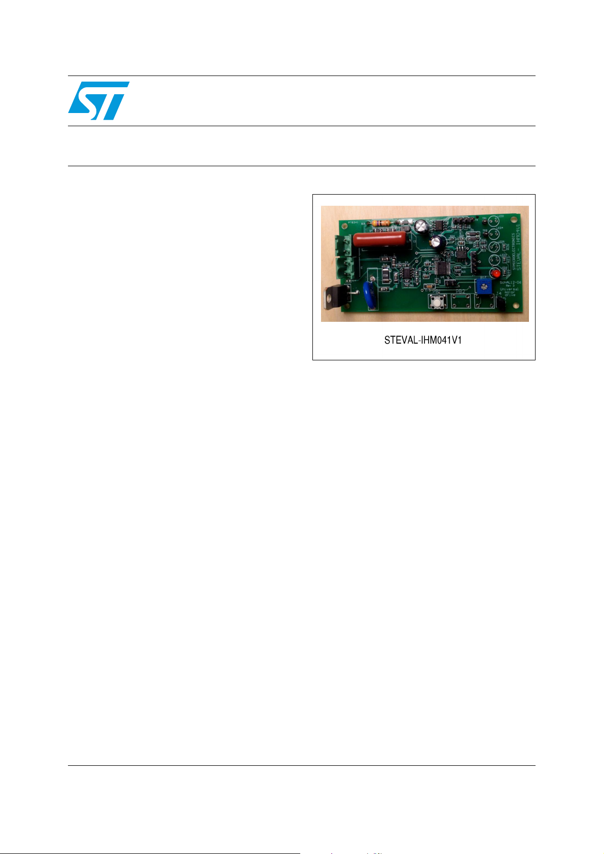
STEVAL-IHM041V1
Databrief
Description
The STEVAL-IHM041V1 demonstration board is a
Triac-based phase angle control for universal
motor speed control using an STM8S103F3P6, 8bit microcontroller, to set the conduction angle of
the Triac.
The STEVAL-IHM041V1 demonstration board
may be operated in either open loop mode or in
closed loop speed control mode, with an AC tach,
Hall sensor or opto-sensor feedback.
The open loop mode may also be used as a lamp
dimmer.
The STEVAL-IHM041V1 demonstration board is
designed to operate from a 120 V/60 Hz mains,
but may be easily modified to operate on other
mains voltages by changing components in the
power supply and motor voltage sensing circuits.
Suggested component values for 230 V/50 Hz
mains voltages are shown in the relevant bill of
materials.
July 2012 Doc ID 023423 Rev 1 1/4
This is information on a product in full production.
www.st.com
4

Schematic diagram STEVAL-IHM041V1
AM12468v1
PB3
DNI
GND
PB2
DNI
PB1
PB1
PB2
PB3
1
2
J2
TX
115VAC
COMMUNICATIONS
out1gnd2gnd3NC
4
NC
5
gnd
6
gnd
7
in
8
U2
L7805ACD13
1
2
P2
R15
47
C4
470F 10V
GND
R16
0.01
10V
Z1
5V
Q1
T1635T
C1
0.22uF
gate
6
5
7
-
+
8
4
U1B
R13
1K
R11
22K
R7
100K
ZC
R17
5K
5V
C3
220uF 10V
MOTOR CONNECTION
POWER SUPPLY
R8
100K
R14
100K
R19
47K
1
2
3
4
J1
swim
C5
0.22uF
GND
5V
C6
0.22uF
LED5
DNI
pd41tx2rx3nrst4oscin5oscout6Vss7Vcap8Vdd9pa3
10
pb5
11
pb4
12
pc3
13
ain2
14
pc5
15
pc6
16
pc7
17
swim
18
ain3
19
ain4
20
U4
STM8S103F3P6
GND
5V
swim
TX
R18
2.2K
R25
2.2K
PB1
PB2
PB3
ZC
VFB
R26
2.2K
R20
100
R21
100
R22
2.2K
R23
2.2K
LED3
DNI
LED2 Red LED
LED4
DNI
LED1
DNI
gate
5V
5V
DEBUG
5V
CURRENT SENSIN G
6
5
7
-
+
8
4
U3B
MOTOR VOLTAGE SENSING
GND
5V
GND
2
3
1
-
+
8
4
U1A
R6
39K
R3 39K
R1 1K
R9 2K
GND
5V
VFB
R10 2K
5V
10R4DNI
R5
39K
R2 39K
2
3
1
-
+
8
4
U3A
LM393
R24
10K
5V
R30
10
VFB
C7
47nF
GND
1
2
3
4
J3
R32
10K
5V
R31
2K
R28
22K
5V
R33
10K
R29
2K
R27
200K
TACHOMETER INTERFACE
R12
MOV
1
TP1
1
TP2
D1
1N4148
D2
D3
C2
2.2uF 250V
1
2
P1
1
2
J4
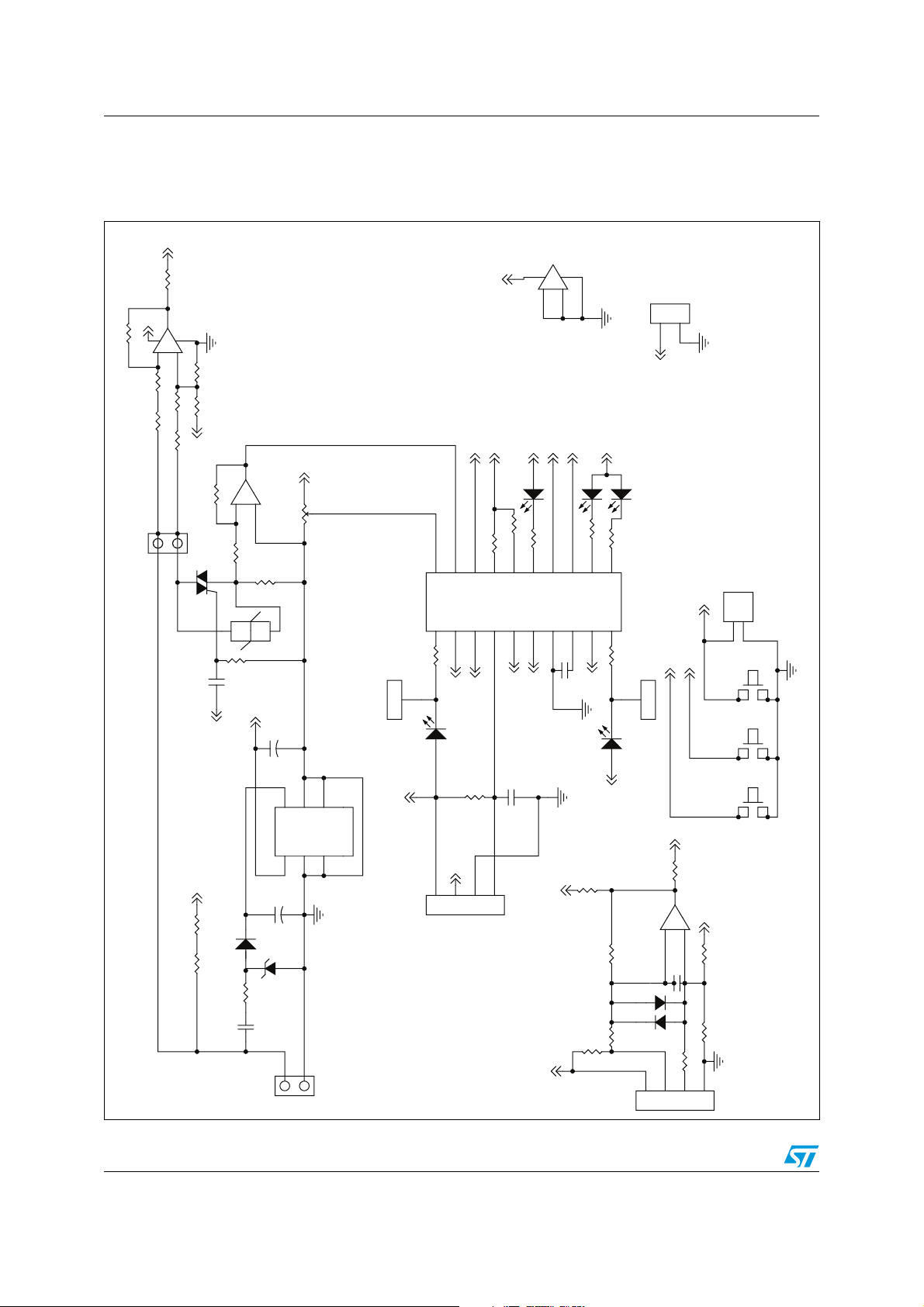
1 Schematic diagram
Figure 1. Schematic diagram
2/4 Doc ID 023423 Rev 1

STEVAL-IHM041V1 Revision history
2 Revision history
Table 1. Document revision history
Date Revision Changes
06-Jul-2012 1 Initial release.
Doc ID 023423 Rev 1 3/4

STEVAL-IHM041V1
Please Read Carefully:
Information in this document is provided solely in connection with ST products. STMicroelectronics NV and its subsidiaries (“ST”) reserve the
right to make changes, corrections, modifications or improvements, to this document, and the products and services described herein at any
time, without notice.
All ST products are sold pursuant to ST’s terms and conditions of sale.
Purchasers are solely responsible for the choice, selection and use of the ST products and services described herein, and ST assumes no
liability whatsoever relating to the choice, selection or use of the ST products and services described herein.
No license, express or implied, by estoppel or otherwise, to any intellectual property rights is granted under this document. If any part of this
document refers to any third party products or services it shall not be deemed a license grant by ST for the use of such third party products
or services, or any intellectual property contained therein or considered as a warranty covering the use in any manner whatsoever of such
third party products or services or any intellectual property contained therein.
UNLESS OTHERWISE SET FORTH IN ST’S TERMS AND CONDITIONS OF SALE ST DISCLAIMS ANY EXPRESS OR IMPLIED
WARRANTY WITH RESPECT TO THE USE AND/OR SALE OF ST PRODUCTS INCLUDING WITHOUT LIMITATION IMPLIED
WARRANTIES OF MERCHANTABILITY, FITNESS FOR A PARTICULAR PURPOSE (AND THEIR EQUIVALENTS UNDER THE LAWS
OF ANY JURISDICTION), OR INFRINGEMENT OF ANY PATENT, COPYRIGHT OR OTHER INTELLECTUAL PROPERTY RIGHT.
UNLESS EXPRESSLY APPROVED IN WRITING BY TWO AUTHORIZED ST REPRESENTATIVES, ST PRODUCTS ARE NOT
RECOMMENDED, AUTHORIZED OR WARRANTED FOR USE IN MILITARY, AIR CRAFT, SPACE, LIFE SAVING, OR LIFE SUSTAINING
APPLICATIONS, NOR IN PRODUCTS OR SYSTEMS WHERE FAILURE OR MALFUNCTION MAY RESULT IN PERSONAL INJURY,
DEATH, OR SEVERE PROPERTY OR ENVIRONMENTAL DAMAGE. ST PRODUCTS WHICH ARE NOT SPECIFIED AS "AUTOMOTIVE
GRADE" MAY ONLY BE USED IN AUTOMOTIVE APPLICATIONS AT USER’S OWN RISK.
Resale of ST products with provisions different from the statements and/or technical features set forth in this document shall immediately void
any warranty granted by ST for the ST product or service described herein and shall not create or extend in any manner whatsoever, any
liability of ST.
ST and the ST logo are trademarks or registered trademarks of ST in various countries.
Information in this document supersedes and replaces all information previously supplied.
The ST logo is a registered trademark of STMicroelectronics. All other names are the property of their respective owners.
© 2012 STMicroelectronics - All rights reserved
STMicroelectronics group of companies
Australia - Belgium - Brazil - Canada - China - Czech Republic - Finland - France - Germany - Hong Kong - India - Israel - Italy - Japan -
Malaysia - Malta - Morocco - Philippines - Singapore - Spain - Sweden - Switzerland - United Kingdom - United States of America
www.st.com
4/4 Doc ID 023423 Rev 1
 Loading...