

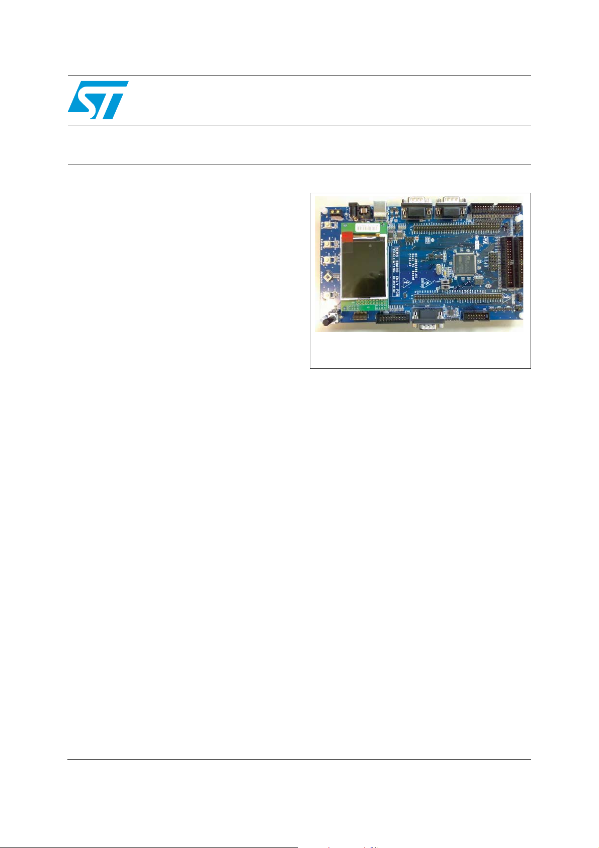
High density dual motor control demonstration board
based on the STM32F103ZE microcontroller
Features
■ Four 5 V power supply sources: 2-way screw
connector, power jack, USB connector or
daughterboard
■ Boot from system or user Flash
■ 64 Mb serial Flash included
■ Two RS-232 channels with RTS/CTS
handshake support on one channel
■ USB 2.0 full speed connection
■ CAN 2.0 A/B compliant connection
■ Two full featured motor control connectors for
field oriented control plus PFC support on one
connector
■ JTAG, SWD and trace debug support
■ 240 x 320 TFT color LCD
■ Joystick with 4-direction control and selector
■ Reset, wakeup, tamper and user button
■ Extension connectors for daughterboard or
wrapping board
■ RoHS compliant
STEVAL-IHM022V1
Data brief
STEVAL-IHM022V1
AM00159V1
Extension headers make it easy to connect a
daughterboard or wrapping board for specific
applications.
Description
The STEVAL-IHM022V1 demonstration board is
designed as a dual motor control development
platform for STMicroelectronics’ ARM Cortex™M3 core-based STM32F103ZE microcontroller.
The board features full speed USB 2.0 and CAN
2.0 A/B compliant interfaces, 2 I
2
I
C channels, 5 USART channels, 3 SPI
channels, 2 DAC channels, internal 64 Kb SRAM
and 512 Kb Flash memory, and JTAG and SWD
debugging support.
The board is designed to implement multiple
motor control (up to three MC connectors are
available) and offers an advanced user I/O
interface (LCD QVGA display and joystick key).
July 2009 Doc ID 16072 Rev 1 1/13
For further information contact your local STMicroelectronics sales office.
2
S channels, 2
www.st.com
13
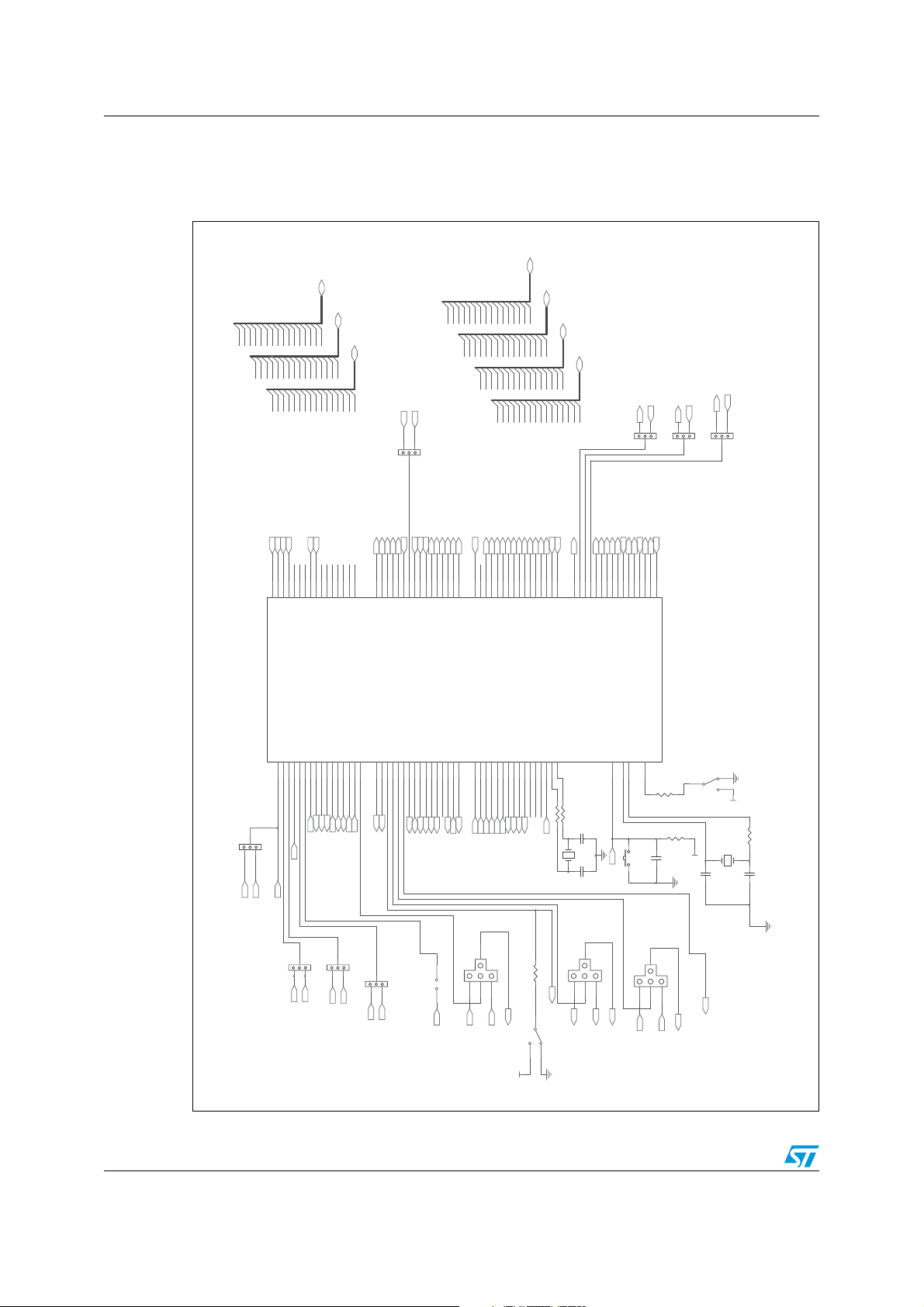
STEVAL-IHM022V1 schematic diagrams STEVAL-IHM0022V1
1 STEVAL-IHM022V1 schematic diagrams
Figure 1. STM32F103ZE microcontroller
PD[0..15]
PG[0..15]
PF[0..15]
PG[0..15]
PG3
PG9
PG10
PG13
PG1
PG0
PG2
PF0
PG12
PG4
PG6
PG5
PG7
PG11
PG8
PF7
PF1
PF2
PF5
PF4
PF6
PF8
PF9
PF10
PF3
PE0
PE2
PE4
PE3
PE5
PE7
PE6
PE1
PE[0..15]
PG15
PG14
PF[0..15]
PF11
PF13
PF12
PF15
PF14
PE[0..15]
PE12
PE11
PE10
PE9
PE14
PE13
PE15
PE8
JMP7
Potentiom eter
123
PD0
PD1
MC_Sub2 Bus Volt age
PD10
PD9
PD2
PD3
PD4
PD6
PD5
PD7
PD8
PC0
PC1
PC4
PC2
PC3
PC5
PC7
PC6
PB1
PB0
PB2
PB4
PB3
PA1
PA0
PC[0..15]
PD[0..15]
PD11
PD13
PD12
PC10
PC9
PC8
PB5
PB7
PB6
PA2
PA3
PA4
PB[0..15]
PD15
PD14
PC[0..15]
PC12
PC11
PC14
PC15
PC13
PB9
PB8
PB10
PA5
PA6
PA7
PA[0..15]
PB[0..15]
PB12
PB14
PB11
PB13
PB15
PA[0..15]
PA8
PA9
PA10
PA11
PA12
PA13
PA14
PA15
JMP8
MC_Sub2 PWM_WL
123
MC_Sub1 EncInde x
JMP9
MC_Sub2 PWM_VL
123
MC_Su b2 PWM_U L
MC_Sub1 EncA
MC_S ub1 En cB
123
JMP10
LED3
IOS_IN7
JOY_Down
JOY_Up
JOY_Select
User_Button
JOY_Right
JOY_Left
PG4
PG6
PG7
PG10
PG11
PG5
PG8
PG9
PG12
PG13
PG14
PG15
128
132
129
126
125
124
127
PG9
PG893PG792PG691PG590PG489PG388PG287PG157PG0
PG13
PG12
PG15
PG14
PG11
PG10
U8A
PA5/ADC12_IN5/D AC_OUT2
PA8
PA2
JMP4
40
PA3
PA4
MC_Main Bus Voltage
123
MC_Sub2 EncB
PA9/USART1_TX
PA6/TIM8_BKIN42PA7/TIM8_CH1N
41
43
100
101
102
PA7
PA8
PA6
PA9
PA10
PA5
USART1_TX
LCD BL_C ontrol
MC_Sub1 PWM_UL
MC_Sub1 Emergenc y Stop
JMP5
123
MC_Main EncB
PA0-WKUP/TIM5_CH134PA1/TIM5_CH235PA2/TIM5_CH336PA3/ADC123_IN337PA4/ADC12_IN4/D AC_OUT1
PA1
PA0
2
JMP3
1
3
WakeUp
MC_Sub2 EncA
MC_Main EncA
IOS_IN8
IOS_IN6
PG3
PA10/USART1_RX
PA11/USBDM
103
PA11
USB_DM
USART1_RX
MC_Sub2 EncIndex
PF13
PF14
PF15
PG0
PG1
PG2
56
PF1555PF1454PF1353PF1250PF11
PA12/USBDP
PA13/JTMS-SWDIO
PA14/JTCK- SWCLK
PA15 /J TDI /T IM2_ CH 1_E TR/ SPI 1_ NSS
PB0/TIM8_CH2N46PB1/TIM8_CH3N47PB2/BOOT1
48
104
105
109
110
PB2
PA12
PA13
PA14
PA15
PB0
PB1
USB_DP
TIM8_ CH 3N
JTMS/SWDIO
JTCK/SWCLK
MC_Sub1 PWM_VL
JMP6
123
MC_Main EncIndex
MC_Main PFC_Ia c
MC_Sub2 Heatsink Temp
IOS_IN2
LED4
LED1
LED2
IOS_IN3
IOS_IN4
IOS_IN5
MC_Main Heatsin k Temp
MC_Sub1 Heats ink Temp
ADC3_IN 6
MC_Sub2 Current A
PF9
PF10
PF6
PF7
PF5
PF8
PF11
PF12
18
49
22
PF9/AD C3_IN721PF8/AD C3_IN620PF7/AD C3_IN519PF6/AD C3_IN4
PF10/AD C3_IN8
PB3/JTDO/SWD_SWO/ TIM2_CH2/SPI1_SCK
PB4/JTRST/TIM3_CH1/SPI1_MISO
PB6/I2C1_SCL
PB9
PB5/I2C1_SMBA1/SPI1_MOSI
PB7/I2C1_SDA
PB8
134
140
137
139
133
135
136
PB6
PB7
PB3
PB8
PB4
PB9
PB10
PB5
I2C_CLK/IOS_IN0
I2C_DATA/IOS_IN1
MC_Main Dissip. brake
MC_Sub1 Dissip. brake
PF3
PF2
PF4
PF515PF414PF313PF212PF111PF0
PB10/TIM2_CH369PB11/TIM2_CH470PB12/SPI2_NSS
73
PB12
PB11
PB13
LCD_SCL
MC_Sub2 PWM_VRef
MC_Sub2 PWM_WRef
JP13
MC_Main PFC_Vac
MC_Main Emergency Stop
PE14
PE13
PE15
PF0
PF1
66
67
68
10
PE14
PE15/TIM1_BKIN
PB15/SPI2_MOSI
PC1/ADC123_IN 1127PC2/ADC123_IN 1228PC3/ADC123_IN 1329PC4/ADC12_IN 1444PC5/ADC12_IN 15
PB13/SPI2_SCK74PB14/SPI2_MISO
PC0/ADC123_IN 10
76
75
26
PB15
PC0
PC1
PC2
PB14
LCD_SDI
LCD_SDO
MC_Sub1 Current A
MC_Main CurrentA
4
Default: jumper
on 2-3 pins
JP14
231
MC_Sub2 Emergenc y Stop
TRACE_D2
MC_Main PWM_UL
TRACE_CK
MC_Sub2 Diss ip. brake
TRACE_D1
TRACE_D3
MC_Main PWM_UH
MC_Main PWM_VH
MC_Main PWM_VL
MC_Main PWM_WL
MC_Main PWM_WH
PE7
PE6
PE12
PE8
PE9
PE5
PE11
PE10
65
63
64
60
59
PE758PE65PE54PE43PE32PE21PE1
PE9/TIM1_CH1
PE13/TIM1_CH3
PE11/TIM1_CH2
PE8/TIM1_CH1N
PE12/TIM1_CH3N
PE10/TIM1_CH2N
PC8/TIM8_CH3
PC7/TIM8_CH2
PC6/TIM8_CH1
PC9/TIM3_CH499PC10
45
97
96
98
111
PC10
PC3
PC4
PC5
PC6
PC7
PC8
PC9
TIM8_C H3
ADC12_IN14
MC_Main CurrentC
MC_Main CurrentB
MC_Sub1 Current C
MC_Sub1 PWM_UH
MC_Su b1 PWM_VH
MC_Mai n PFC _PWM
CON3+1_1
SW4
JTDI
SPI1_NSS
+3V3
LCD_WR
MC_Sub2 Emergency Stop
TRACE_D0
MC_Main PFC_OCP
PD12
PD14
PD15
PE0
PE1
PD13
PE3
PE4
PE2
86
141
142
81
PD15
PE0/TIM4_ETR
PD14/TIM4_CH 385PD13/TIM4_CH 282PD12/TIM4_CH 1
PC13/ANTI-TAMP
PC11
PC12
PC14/OSC32-IN8PC15/OSC32-OUT
7
9
112
113
PC14
PC15
PC12
PC11
PC13
R89
R90
0R
0R
C56
10pF
Y1
Anti_Tamper
32.768 Khz
10pF
C55
4
Default: jumper
on 1-2 pins
R88
100K
JP15
231
LCD_CS
BOOT1
JTDO
MC_Sub1 NTC By pass relay
PD11
80
PD11
MC_Sub2 PWM_URef
MC_Sub2 NTC By pass relay
MC_Ma in N TC By pas s rel ay
PD9
PD10
79
PD978PD8
PD10
CON3+1_1
USART2_TX
USART2_RX
LCD_RS
USB_Disconnect
PD5
PD6
PD8
PD7
77
122
123
119
PD7
PD6/USART2_RX
NRST25OSC_IN23OSC_OUT24BOOT0
RESET
OSC_IN
OSC_OUT
S1
RESET
SP1_SCK
USART2_CTS
USART2_RTS
CAN_RX
CAN_TX
MC_Main PFC Sy nc2
PD2
PD3
PD4
PD0
PD1
114
118
117
115
116
PD1/CANTX
PD0/CA NRX
PD2/TIM3_ETR
PD5/USART2_TX
PD4/US ART2_RTS
PD3/US ART2_CTS
STM32F103ZET6
138
R91
C57
100nF
RESET
4
JP16
231
JTRST
SPI1_MISO
BOOT0
SW5
100K
+3V3
R93
R92 10K
+3V3
C58
CON3+1_1
SPI1_MOSI
MC_Main PFC_Sy nc1
390R
8MHz
Y2
22pF
C59
22pF
AM00164v1
2/13 Doc ID 16072 Rev 1
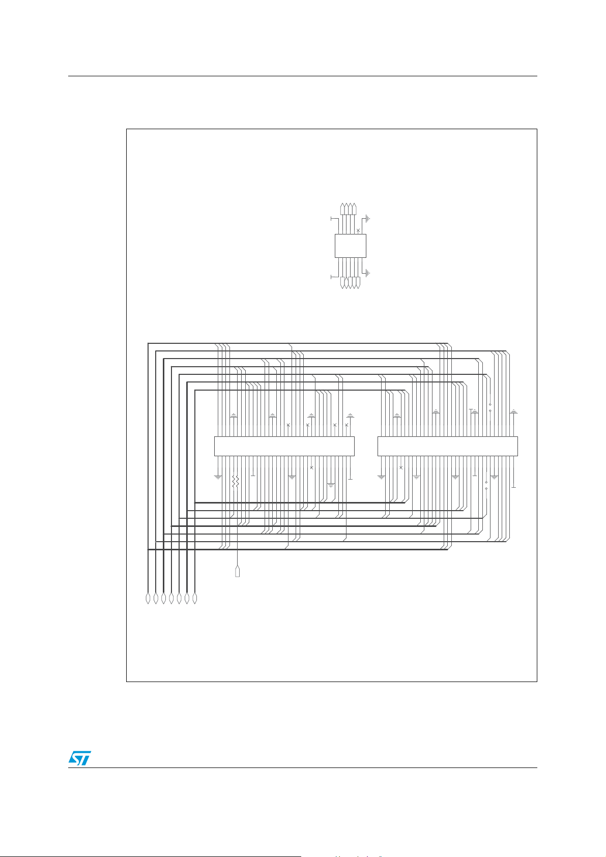
STEVAL-IHM0022V1 STEVAL-IHM022V1 schematic diagrams
Figure 2. Extension and I2C connectors
IOS_IN8
IOS_IN5
IOS_IN6
IOS_IN7
+5V
PF12
PF14
PF15
PF13
I2C_IOS
CON2
1 2
345 6
91011 12
13 14
7 8
PF4
PF5
PB6
PF11
PB7
+5V
IOS_IN2
IOS_IN4
IOS_IN3
I2C_CLK/IOS_IN0
I2C_DATA/IOS_IN1
PC15
PD9
PG2
PG4
PG6
PG8
CON1
PC[0.. 15]
PF[0. .15]
PG[0.. 15]
PE[0.. 15]
PF[0..15]
PG[0..15]
PA[0.. 15]
PD[0.. 15]
PB[0.. 15]
PB[0..15]
PD[0..15]
PC[0..15]
PE[0..15]
PA[0..15]
PB15
PB14
PD11
PD13
1 2
3 4
567 8
9 10
111213 14
17 18
15 16
R1
R2
820
820
PD12
PD8
PG7
PG5
PG3
PD10
PC13
RESET
PE8
PG0
PF15
PE12
PE10
PB12
PB10
PE14
PD14
32
19 20
21 22
23 24
D5V
PB13
PB11
39 40
252627 28
29 303133 34
37 38
35 36
PF14
PE13
PE11
PE9
PE7
PG1
PD15
PE15
PA3
PA2
PF11
PF13
41 42
43 44
45 46
PB1
PF12
PB2
PC2
PC5
PC0
PA7
PA5
70
49 50
47 48
51 52
535455 56
57 58
5960616263 64
6566676869
Header 35 x 2
+3V3
PC4
PC3
PC1
PB0
PA6
PA4
PA1
PF10
PA11
PC6
PA10
PA8
PA13
PC8
10
CON3
1 2
3 4
5 6
789
13 14
11 12
PC7
PC9
PA12
PA0
PA9
PG9
PG13
PG11
PD1
PD3
PD5
PC12
PC11
PA15
PE1
15 16
17 18
19 20
21 22
PC10
PE2
PD0
PA14
PB3
PB5
PB7
PB9
PG15
34
32
25 26
23 24
27 28
29 303133
35 36
37 38
3940414243 44
PG14
PB4
PD4
PD2
PB6
PD6
PD7
PG10
PB8
PG12
PF3
PE3
PC13
PF9
PF7
PF5
PE5
PF1
+3V3
JP2
45 46
4748495051 52
535455 56
5758596061 62
636465 66
67 68
69 70
Header 35 x 2
D5V
JP1
+3V3
PF0
PE0
PE4
PF2
PE6
PF4
PF8
PF6
PC14
AM03542v1
Doc ID 16072 Rev 1 3/13
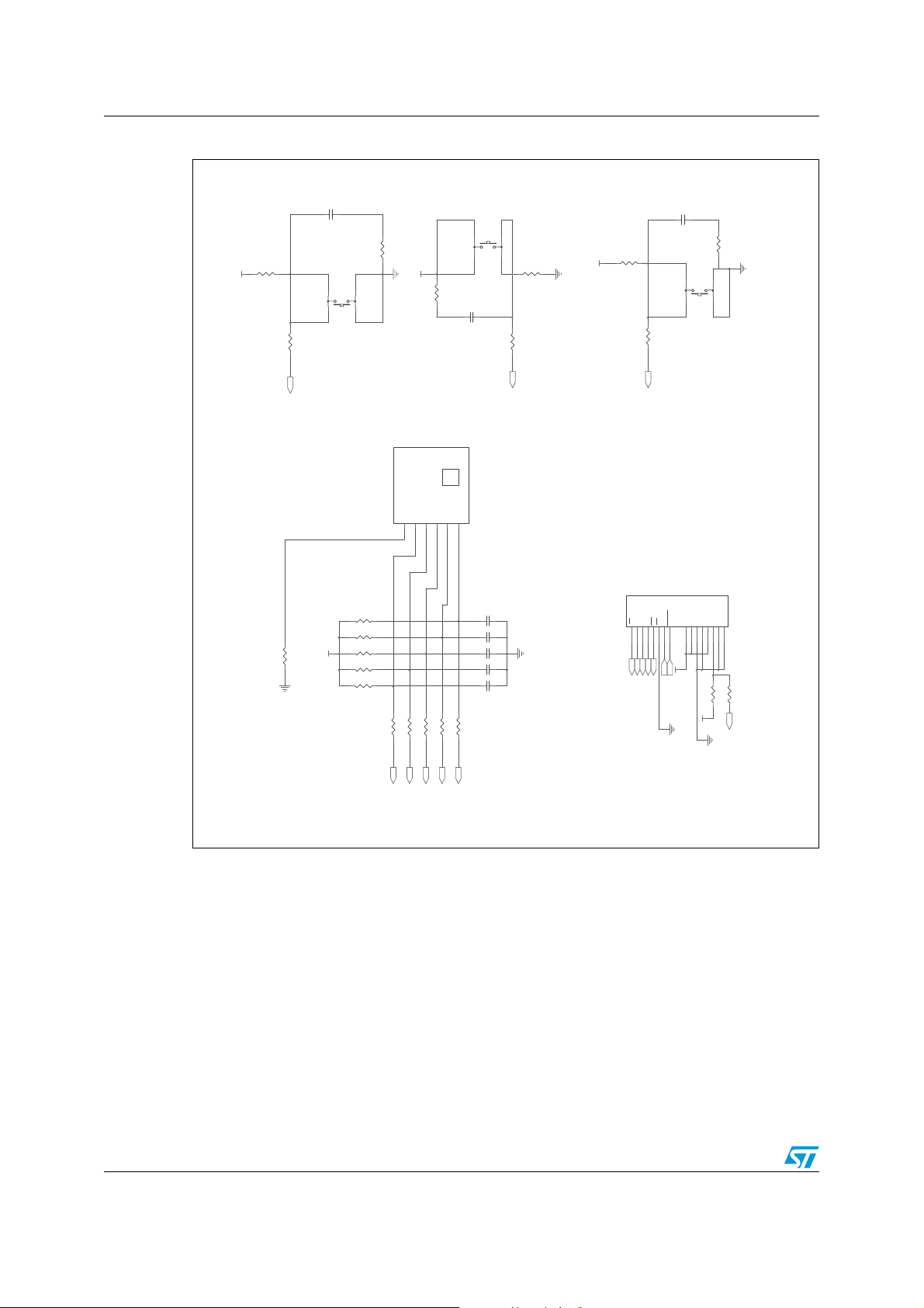
STEVAL-IHM022V1 schematic diagrams STEVAL-IHM0022V1
Figure 3. Joystick, buttons and LCD connections
100nF
C1
WAKE-UP
1
2
R11
4k7
R3
+3V3
3
2
100R
4
SW1
1
SW2
4
3
220K
R19
+3V3
100R
R16
do not f it
C2
R20
4K7
+3V3
C8
100nF
100R
R23
3
4
SW3
2
1
USER
R5
Anti_Tamper
R4
ANTI-TAMPER
0R
Joystick
DOWN3RIGHT
COMMON
U1
10K
R10
R9
10K
R8
10K
+3V3
100R
R7
10K
10K
R6
R120R
LEFT1Selection
5
2
6
0R
0R
R13
R150R
R14
R17 0R
R18
330R
WAKEUP
MT008-A
UP
4
C7
100nF
C6
100nF
C5
100nF
C4
100nF
C3
100nF
0R
R21
User_Button
VCI
GND
GND
BL_VDD13BL_Control14BL_GND15BL_GND
SCL
CON4
3
1CS2
LCD_CS
LCD_SCL
VDD
SDO
WR
SDI
RESET
9
6RD7
4RS5
8
+3V3
RESET
LCD_RS
LCD_WR
LCD_SDO
LCD_SDI
Color LCD Module
10
11
16
12
R24
R22
do not f it
0R
+3V3
LCD BL_Contr ol
JOY_Select
JOY_Right
JOY_Up
JOY_Left
JOY_Down
4/13 Doc ID 16072 Rev 1
AM03543v1

STEVAL-IHM0022V1 STEVAL-IHM022V1 schematic diagrams
Figure 4. JTAG and trace connectors
R30
do not f it
+3V3
R33
10k
10k
10k
Default setting:Open
JP3
+3V3
2
1
456
7891011
3
R28
10K
R27
10K
10K
R26
10K
R25
+3V3
CON6
R29
10K
+3V3
R34
R35
14
15
19
12
18
13
16
17
20
JTAG
R32
do not f it
R31
do not f it
R37
0R
0R
R36
AM00160v1
1234567
JTDI
JTDO
JTRST
RESET
JTCK/SWCLK
JTMS/SWDIO
CON5
89101112
13
17
18
16
14
15
20
19
TRA CE
Doc ID 16072 Rev 1 5/13
TRACE_D 2
TRACE_D 0
TRACE_C K
TRACE_D 1
TRA CE_ D3

STEVAL-IHM022V1 schematic diagrams STEVAL-IHM0022V1
Figure 5. Motor control connector main
MC_Main Bus Voltage
MC_Main PFC_OCP
MC_Main PFC_Vac
MC_Main PFC_Iac
R43
4
PFC OCP_Sense
EMERGENCY STOP
1 2
3
MC_UH
GND
do not f it
R44
C11
22nF
4.7K
18
202224
GND
GND
GND
GND
GND
GND
BUS VOLTAGE
MC_WH
MC_VL
MC_VH
MC_WL
MC_UL
5 6
CURRENT B
CURRENT A
9 10
7 8
13 14
15 161719
11 12
100K
R42
C9
100nF
0R
R40
R39
100K
Motor control connector
CON8
R46
GND
PFC Vac_sense
PFC Iac_sense
CURRENT C
NTC BYPASS RELAY
DISSIPATIVE BRAKE
21
23
R47
C13
0R
3.3V Power
Heatsink Temperature
PFC SYNC
+5V POWER
25 26
29 30
27 28
+5V
GND
PFC PWM
do not f it
do not f it
31 32
GND
ENCODER A
Encoder Index
ENCODER B
33 34
C15
100nF
MC_Main EncIndex
do not f it
C19
do not f it
C18
do not f it
C17
C21
JP4
10nF
MC_Main Heatsink Temp
R49
0R
+3V3
MC_Main connector
Default setting:Open
MC_Main Dissip. brake
C10
R38
3.3K
+3V3
1nF
MC_ Main PW M_U L
MC_ Main PWM_ VH
MC_ Main PW M_U H
R41
0R
MC_Main Emergency Stop
MC_Main NTC Bypas s relay
MC_ Main PWM_ VL
MC_ Main PW M_W L
MC_Main PWM_WH
C12
do not f it
0R
R45
MC_Main Curr entA
6/13 Doc ID 16072 Rev 1
C20
do not f it
MC_Main EncB
MC_Main EncA
MC_Main PFC_PWM
0R
0R
R48
MC_Main CurrentB
R50
do not f it
C14
C16
do not f it
MC_Main CurrentC
C23
do not f it
JP5
C22
Default setting: Closed
do not f it
MC_Main PFC Sy nc2
MC_Main PFC_Sy nc1
AM00161v1

STEVAL-IHM0022V1 STEVAL-IHM022V1 schematic diagrams
Figure 6. Motor control connector sub1
100nF
+3V3
MC_Sub1 EncIndex
JP6
Default setting:Open
C31
do not f it
do not f it
C32
C30
do not f it
10nF
C33
GND
MC_UH
5 6
GND
GND
MC_VH
MC_UL
7 8
GND
MC_VL
9 10
R54
GND
MC_WH
11 12
MC_Sub1 Bus Voltage
14
BUS VOLTAGE
MC_WL
13
GND
CURRENT A
15 16
100K
R55
C26
100nF
0R
18
20
24
22
GND
GND
PFC Vac_sense
PFC Iac_sense
CURRENT C
DISSIPATIVE BRAKE
NTC BY PASS RELAY
CURRENT B
1719212325
26
Heatsink Temperature
+5V POWER
+5V
ADC3_IN6
246
Jumper Double 6 pin
J2
1
3
5
Default position: 1-3 a nd 2-4
ADC12_IN 14
MC_Sub1 CurrentB
MC_Sub1 Bus Voltage
GND
EMERGENCY STOP
CON9
1 2
3 4
MC_Sub1 Heatsink Temp
C28
R57
0R
GND
GND
3.3V Power
Encoder Index
PFC PWM
PFC SYNC
ENCODER B
ENCODER A
MC_Sub1 connector
33 34
29 30
31 32
27 28
MC_Sub1 EncB
C24
R51
3.3K
+3V3
1nF
MC_Sub1 PWM_UL
MC_Sub1 PWM_VH
MC_Sub1 PWM_UH
MC_Sub1 PWM_VL
R52
0R
0R
R53
4
2
6
Jumper Double 6 pin
J1
1
5
MC_Sub1 Emergency Stop
3
TIM 8_C H3 N
TIM8_CH3
Default position: 1-3 and 2-4
MC_Sub1 EncA
MC_Sub1 Dissip. brake
MC_Sub1 NTC By pass relay
0R
R58
0R
R56
C25
do not f it
MC_Sub1 CurrentA
C27
do not f it
MC_Sub1 CurrentB
C29
do not f it
MC_Sub1 CurrentC
AM00162v1
Doc ID 16072 Rev 1 7/13

STEVAL-IHM022V1 schematic diagrams STEVAL-IHM0022V1
Figure 7. Motor control connector sub2
MC_Sub2 PWM_WL
MC_Sub2 PWM_UL
MC_Sub2 PWM_VL
MC_Sub2 Aux
9
8
7
6
5
4
3
2
1
CON14
Male connector
MC_Sub2 Bus Volta ge
100K
R63
PC0
C35
100nF
0R
R61
MC_Sub2 Heats ink Temp
C37
R64
0R
100nF
MC_Sub2 EncIndex
C39
do not f it
34
Encoder Index
ENCODER B
33
MC_Sub2 EncB
+3V3
C40
do not f it
C38
JP7
Default setting:Open
do not f it
C41
10nF
MC_Sub2 connec tor
MC_ Su b2 P WM_ VH
MC_Sub2 PWM_VRef
MC_Sub2 PWM_UH
MC_Sub2 PWM_URef
MC_Sub2 PWM_WH
MC_Sub2 PWM_WRef
10
2
GND
GND
MC_UL
MC_UH
EMERGENCY STOP
CON10
3 4
56789
1
C34
R59
3.3K
+3V3
1nF
MC_Sub2 PWM_UL
MC_Sub2 PWM_UH
R60
0R
182022
GND
GND
GND
GND
GND
GND
GND
BUS VOLTAGE
CURRENT A
MC_VL
MC_WH
CURRENT B
CURRENT C
MC_WL
MC_VH
15 16
1719212325 26
11 12
13 14
MC_Sub2 PWM_VL
MC_Sub2 PWM_VH
MC_Sub2 PWM_WL
MC_ Su b2 P WM_ W H
0R
R62
24
PFC Vac_sense
NTC BY PASS RELAY
MC_Sub2 NTC By pass relay
C36
PFC Iac_sense
Heatsink Temperature
DISSIPATIVE BRAKE
+5V POWER
27 28
+5V
MC_Sub2 Diss ip. brak e
do not f it
32
GND
3.3V Power
PFC PWM
PFC SYNC
293031
GND
ENCODER A
MC_Sub2 EncA
MC_Sub2 CurrentA
MC_Sub2 Emergency Stop
8/13 Doc ID 16072 Rev 1
AM00163v1

STEVAL-IHM0022V1 STEVAL-IHM022V1 schematic diagrams
Figure 8. Peripherals
RV1
10K
+3V3
C44
100nF
D2 Orange
D3 Green
D1 Red
R66
R65
600R
LED2
LED1
D4 Blue
R71
R69
600R
600R
600R
LED3
LED4
R76
0R
Potentiometer
U4
C46
+3V3
100nF
C
HOLD
+3V3
4567
3
D
W
Q
VCC
S VSS
M25P64-VME6G
2
1
8
R79
0R
0R
R81
SPI1_MISO
SP1_SCK
SPI1_NSS
SPI1_MOSI
LED
Potentiometer
USB
P1
USB_DM
USB_DP
22R
R68 22R
R67
+5V
+3V3
C42
100nF
456
I/O1
I/O2
Vbus
I/O2
I/O1
GND
U2
USBLC6-2SC6
123
U5V
1
2
3
456
D-
D+
VCC
GND
SHELL
SHELL
CON11
R74
36K
1.5K
R72
Q1
2STR1215
10K
R73
+3V3
U5V
R70
1MR
C43
4.7nF
USB-ty peB conn.
USB_Disc onnect
123
JMP1
R75
47K
Default setting: 2<->3
Q2
2STR1215
+3V3
R78 0R
JMP2
Default setting: 2<->3
1
2
3
10K
R77
+3V3
1
JP8
JUMPER
Default setting:Open
7
8
RS
D
U3
234 5
1
C45
100nF
CAN_TX
DB9-male connec tor
4
83726
5
9
R84
0R
R83
do not f it
R82
120R
6
CANH
CANL
Vref
GND
SN65HVD230
VCC
R
0R
R80
CAN_RX
SPI Flash
CAN
+3V3
AM03548v1
Doc ID 16072 Rev 1 9/13

STEVAL-IHM022V1 schematic diagrams STEVAL-IHM0022V1
Figure 9. Power supply
C70
100nF
C69
100nF
VDD
C68
100nF
C67
VDD
Default: JP12 present
VDDA
VDD_995VDD_884VDD_762VDD_652VDD_517VDD_439VDD_3
100nF
C66
100nF
C65
100nF
C64
100nF
C63
100nF
C62
100nF
C61
100nF
C60
100nF
L1
BEAD
C54
10nF
+
47R
R86
C53
10uF
VDDA
33
144
108
32
6
VBAT
VDDA
VDD_2
VDD_172VREF+
+3V3
C50
100nF
C51
10uF
+
2
VOUT
GND
1
LD1086D2 M33
U7
VIN
3
470uF 16V
C49
+
+5V
C48
10uF 16v
E5V
+
5
6
4
2
CV
CG1
CG2
CG3
U6
BNX002-01
SG1SV
3
C47
100nF
D5 Red
300R
R85
+5V
JP9
JP11
JP10
JP12
Default setting: jumper present only on JP9 pins
E5VD5VU5V
+3V3
VREF+
C52
470nF
VDD
131
121
VDD_11
VDD_10
U8B
VSS_171VSS_2
VSS_3
VSS_438VSS_516VSS_651VSS_761VSS_883VSS_9
VSS_10
94
107
143
130
1 2
Z1
SMAJ5.0A-TR
3
OUT
GND
2
IN
U5 ZEN056V130A24LS
1
3
2
1
CON12
DC-10B
1
2
Aux DC
CON13
120
VREF-
STM32F103ZET6
VSS_11
VSSA
VREF-
31
30
R87
0R
AM03549v1
10/13 Doc ID 16072 Rev 1

STEVAL-IHM0022V1 STEVAL-IHM022V1 schematic diagrams
Figure 10. RS-232 connectors
DB9-male c onnector
P2
7
261
8
3
R94 do not fit
100nF
C74
100nF
5
16
VCC
U9
V+
100nF
C72
2
C73 100nF
C71
+3V3
10
4
5
9
USART2
7
14
4
15
13
8
C2-
C2+
R1in
R2in
GND
T2ou t
T1ou t
C1+1C1-
R1out
R2out9V-
T1in
T2in
ST3232EBTR
6
3
12
10
11
C75
100nF
0R
R95 0R
R96
+3V3
P3
6
7
1
2
R97 do not fi t
C76
100nF
C77
C78
U10
100nF
100nF
4
9
3
8
4
5
14
16
C2-
C2+
VCC
V+2C1+1C1-3T1in11R1out
C79 100nF
DB9-male c onnector
10
R2in
R2out
USART1
15
GND
V-
ST3232EBTR
C80
100nF
6
5
7
13
8
R1in
T2ou t
T1out
T2in
9
10
12
10K
0R
R99
R98
US ART2 _CTS
USART2_RX
US ART2 _RTS
USART2_TX
USART1_RX
USART1_TX
AM03550v1
Doc ID 16072 Rev 1 11/13

Revision history STEVAL-IHM0022V1
2 Revision history
Table 1. Document revision history
Date Revision Changes
29-Jul-2009 1 Initial release.
12/13 Doc ID 16072 Rev 1

STEVAL-IHM0022V1
Please Read Carefully:
Information in this document is provided solely in connection with ST products. STMicroelectronics NV and its subsidiaries (“ST”) reserve the
right to make changes, corrections, modifications or improvements, to this document, and the products and services described herein at any
time, without notice.
All ST products are sold pursuant to ST’s terms and conditions of sale.
Purchasers are solely responsible for the choice, selection and use of the ST products and services described herein, and ST assumes no
liability whatsoever relating to the choice, selection or use of the ST products and services described herein.
No license, express or implied, by estoppel or otherwise, to any intellectual property rights is granted under this document. If any part of this
document refers to any third party products or services it shall not be deemed a license grant by ST for the use of such third party products
or services, or any intellectual property contained therein or considered as a warranty covering the use in any manner whatsoever of such
third party products or services or any intellectual property contained therein.
UNLESS OTHERWISE SET FORTH IN ST’S TERMS AND CONDITIONS OF SALE ST DISCLAIMS ANY EXPRESS OR IMPLIED
WARRANTY WITH RESPECT TO THE USE AND/OR SALE OF ST PRODUCTS INCLUDING WITHOUT LIMITATION IMPLIED
WARRANTIES OF MERCHANTABILITY, FITNESS FOR A PARTICULAR PURPOSE (AND THEIR EQUIVALENTS UNDER THE LAWS
OF ANY JURISDICTION), OR INFRINGEMENT OF ANY PATENT, COPYRIGHT OR OTHER INTELLECTUAL PROPERTY RIGHT.
UNLESS EXPRESSLY APPROVED IN WRITING BY AN AUTHORIZED ST REPRESENTATIVE, ST PRODUCTS ARE NOT
RECOMMENDED, AUTHORIZED OR WARRANTED FOR USE IN MILITARY, AIR CRAFT, SPACE, LIFE SAVING, OR LIFE SUSTAINING
APPLICATIONS, NOR IN PRODUCTS OR SYSTEMS WHERE FAILURE OR MALFUNCTION MAY RESULT IN PERSONAL INJURY,
DEATH, OR SEVERE PROPERTY OR ENVIRONMENTAL DAMAGE. ST PRODUCTS WHICH ARE NOT SPECIFIED AS "AUTOMOTIVE
GRADE" MAY ONLY BE USED IN AUTOMOTIVE APPLICATIONS AT USER’S OWN RISK.
Resale of ST products with provisions different from the statements and/or technical features set forth in this document shall immediately void
any warranty granted by ST for the ST product or service described herein and shall not create or extend in any manner whatsoever, any
liability of ST.
ST and the ST logo are trademarks or registered trademarks of ST in various countries.
Information in this document supersedes and replaces all information previously supplied.
The ST logo is a registered trademark of STMicroelectronics. All other names are the property of their respective owners.
© 2009 STMicroelectronics - All rights reserved
STMicroelectronics group of companies
Australia - Belgium - Brazil - Canada - China - Czech Republic - Finland - France - Germany - Hong Kong - India - Israel - Italy - Japan -
Malaysia - Malta - Morocco - Philippines - Singapore - Spain - Sweden - Switzerland - United Kingdom - United States of America
www.st.com
Doc ID 16072 Rev 1 13/13
 Loading...