

User interface for home appliance / S-Touch™ daughter
Features
■ 12-bit GPIO device with additional 12-channel
capacitive sensing sensors
■ Interface with MCU through I²C bus.
■ Fast and accurate results at very low power
consumption
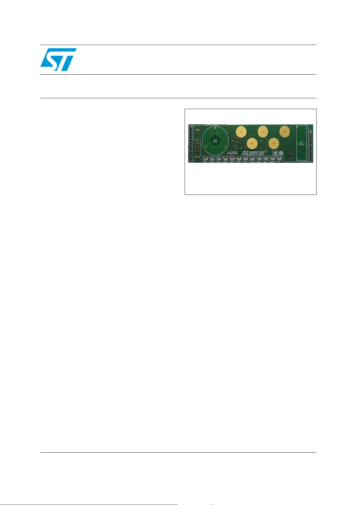
STEVAL-IHI002V1
demonstration board
Data Brief
Description
This demonstration board is designed to
modernize or even fully replace a mechanic
keyboard. The demonstration board is based on
the STMPE1208S device, a 12-bit GPIO
expander with an additional 12-channel capacitive
sensing sensor, which is able to interface a main
MCU through I²C bus. The demonstration board is
designed to work as a daughter board for the
STEVAL-IHI001V1 (washing machine user
interface). Once plugged in, the STEVALIHI002V1 is automatically detected by the mother
board, replacing the mechanic keys by a wheel, a
slider and 5 buttons.
STEVAL-IHI002V1
November 2008 Rev 1 1/4
For further information contact your local STMicroelectronics sales office.
www.st.com
4
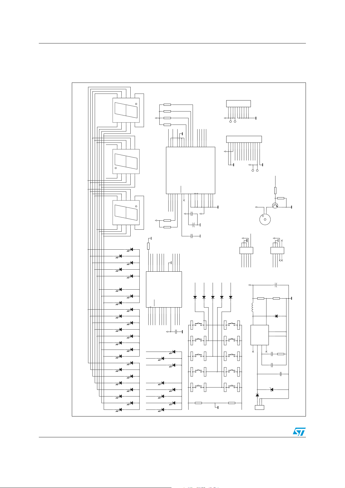
Circuit schematic STEVAL-IHI002V1
1 Circuit schematic
Figure 1. Schematic
10
1
2
6
8
f
e
g
dp
A2
DIG4
DY3
Comm on Anode
d9c7b5a
DIG3
3
A1
DY2
Common Anode
A2
8
DIG3
10
e
DY1
Common Anode
d9c7b5a
SEG8
SEG7
SEG6
SEG5
SEG4
SEG3
SEG2
SEG1
A1
4
3
4
d9c7b5a
e10f2g1dp
6
2
1
6
8
f
g
dp
A2
DIG2
A1
4
3
DL24
R4
DL23
DL21
DL19
DL17
DL15
DL13
DL11
DL9
DL7
DL5
DL3
DL1
390 1%
DL22
24
DL20
DL18
DIG7
DL16
U3
STLED316S
DL14
DIO
DL12
DL10
DIG6
DL8
DL6
DL4
DL2
DIG5
+VDD
U2
+VDD
SEG1
SEG2
SEG3
SEG4
KEY1
KEY2
22
18
ISET
KEY123KEY2
SEG1/KS121SEG2/KS220SEG3/KS319SEG4/KS4
DIN/DOUT1CLK2STB3IRQ_N4DIG1/LED5DIG26DIG37DIG4
DIG3
IRQ
STB
CLK
DIG1
DIG2
QST
SEG8
SEG7
SEG6
SEG5
SEG4
SEG3
SEG2
DL25
SEG1
R15
10K
5%
R14
10K
5%
R13
10K
5%
R12
10K
5%
TINT
PA2
32
31
30
PA0(HS)
PA1(HS)/ATIC
PA2(HS)/ATPWM
ATPWM1/PA3(HS)1ATPWM2/MCO/PA4(HS)2ATPWM3/PA5(HA)3I2CDATA/PA6(HS)4I2CCLK/PA7(H S)5RESET6NC7VDD
ST7FLI49MK1T6
I2CD
RST0
PA4
PA3
R11
4K7
5%
R10
4K7
5%
SEG5
SEG6
17
15
16
GND
SEG5/KS5
VCC9DIG5
8
10
DIG4
DIG5
+VDD
C6
DL32
DL31
S-TOUCH
STAND ALONE
DL30
DL29
DL28
DL27
DL26
J4
CON10
123456789
+VDD
MD1
MD2
PC2/ICCDATA
22
PC1/AI N923PC0/AI N8
VSS9OSC1/CLKIN
C7
+
C5
C8
D1 1N4148
1
2
1
2
1
2
1
2
1
2
DIO
CLK
PB7/AIN 721PB6/AIN 620PB5/AIN 519PB4/AIN 4
OSC211VSSA12VDDA13AIN0/PB014CKIN/AIN1/PB1
10
+VDD
100nF
10uF
16V
10nF
SEG1
P1
TACT-2
P2
TACT-2
P3
TACT-2
P4
TACT- 2
P5
TACT- 2
R5
10K
BUZ
STB
IRQ
J3
CON15
18
17
PB3/AIN 3
15
SEG2
D2 1N4148
D3 1N4148
4
3
4
3
4
3
4
3
4
3
5%
123456789
+VDD
AIN2/PB2
16
SEG3
SEG4
SEG5
D4 1N4148
D5 1N4148
P6
1
2
P7
1
2
P8
1
2
P9
1
2
P10
1
2
R6
GINT
ICCC
ICCD
25
24
26
27
29
PC628PC5
PC4/LTIC
PC7/BREAK
PC3/ICCC LK
8
I2CC
RST
+VDD
SEG7
SEG8
SEG8/KS813SEG7/KS714SEG6/KS6
DIG611DIG7
12
DIG6
DIG7
100nF
KEY1
DIG1
10
TP4
TP3
1011121314
15
PA4
I2CC
I2CD
RST0
PA3
PA2
MD1
TINT
GINT
MD2
+VDD
TP2
TP1
+VDD
BZ1
+VDD
MD2
12345678910
J5
CON10A
TACT-2
4
3
TACT-2
4
3
TACT-2
4
3
TACT- 2
4
3
TACT- 2
4
3
10K
5%
I2C Expander
I2CD
I2CC
RST0
MD1
RST
+VDD
21
L1
33uH
1
OUT
U4
L5970D
6
D6
1N4007
123
KEY2
J1
CON3
BUZ
R9
4K7 5%
R8
10K
5%
Q1
1
2
BC337
Buzzer
+VDD
12345678910
J2
CON10A
R2
15K
1%
5
FB
GND
INH
SYNC2COMP
VCC8VREF
4
C3
C2
5V-30V
INPUT
ICC Programmer
ICCD
RST
ICCC
C4
100uF
16V
+
R3
4K7
1%
D7
STPS340U
7
3
22nF
R1
4K7
220pF
C1
10uF
35V
TR1
SMAJ33A-TR
2/4
 Loading...