

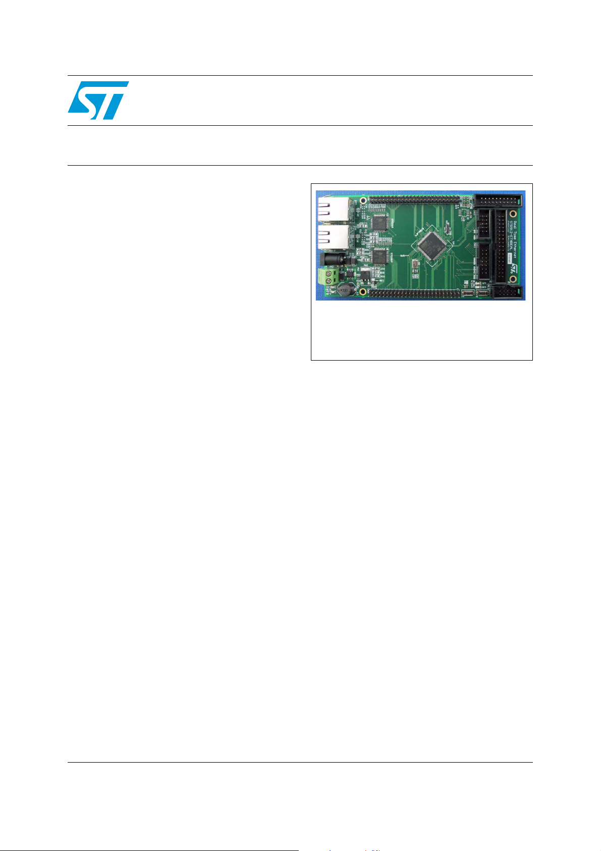
Real-time Ethernet slave node demonstration board
Features
■ 32-bit STR912FAW44 microcontroller with
ARM966E-S™ core running at 96 MHz
■ Two fast E-STE101P Ethernet transceivers
supporting full duplex communication;
available boot configuration settings; up to 32
selectable MII addresses; RJ45 connectors
with embedded LEDs
■ Two 50-pin header connectors for connecting
different on-hook extensions with real-time IP
featuring: three MIIs (medium independent
interface), EMI (external memory interface),
UART, I2C, SPI, external interrupts, 1.8 V, 3.3
V and GND pins
■ Connectors for interfacing with industrial I/O
cards: CAN, AC MC (motor control), CLT/PCLT
(input termination circuit), HSD or SPI HSD
(high side driver)
■ Power supply using the L5973AD DC-DC
converter, and the LF18 for the core supply
■ JTAG debug interface connector
■ 6 V to 30 V DC power supply voltage range
■ One reset and one general-purpose button;
two general purpose LEDs
STEVAL-IFW001V1
based on the STR912FAW44
Data Brief
STEVAL-IFW001V1
For Xilinx® Spartan™ FPGA extensions, refer to
user manual UM0499 for the STEVAL-IFW002V1
demonstration board. With additional on-board
connectors it is possible to connect industrial I/O
cards and motor control boards.
Description
This demonstration board based on
STR912FAW44 was designed for real-time
Ethernet slave communication node evaluation.
This board can be daisy chained with others into
factory automation field bus systems. The board
enables and requires the hooking on of different
extensions that fulfill the requirements for different
real-time Ethernet protocols on the market (e.i.
Powerlink, EtherCAT, and others). For each
protocol a special extension, or a programmable
extension, must be used. The communication
between the board and the extension can be
accomplished through MII, EMI, SPI™, I2C™ or
UART.
September 2008 Rev 1 1/9
For further information contact your local STMicroelectronics sales office.
www.st.com
9
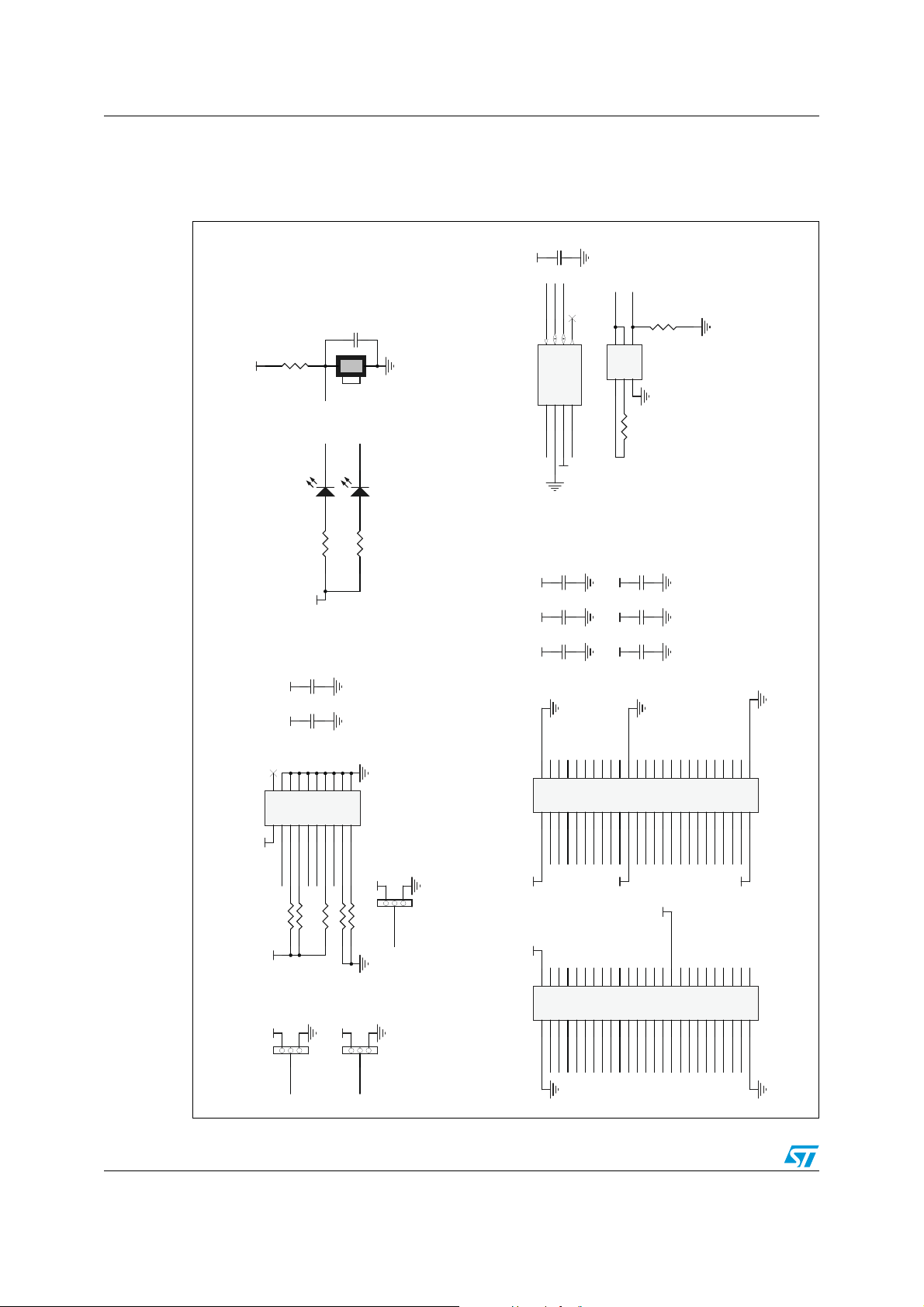
Demonstration board schematic STEVAL-IFW001V1
1 Demonstration board schematic
Figure 1. Connectors, buttons, LEDs and CAN
C6
100nF
3V3
CAN_H
CAN_L
CAN_RS
C10
10nF
R5
10K
LD1
yellow
21
P56
P20
LD2
1 2
yellow
B1
GM: P-DT2112C
P21
1 2
3V3
CAN
U1
7
8
RS
CANH
D1GND2VCC3R
P51
6
5
CANL
4
P50
3V3
Vref
CAN_RS
R11
10K
1 2
3 4
5 6
CN2
Header 3X2
SN65HVD230
CAN_L CAN_H
5-6 HI/LOW speed
R14
100
R12
300
R13
300
C5
100nF
1V8
GP LEDs and Buttons
CN1
3V3
3V3
C2
100nF
3V3
C1
100nF
3V3
1 2
3 4
5 6
7 8
9 10
11 12
13 14
15 16
17 18
19 20
GM: MLW20G
JTRST
JTDI
JTMS
JTCK
JRTCK
JTDO
RESET_IN
DBGRQ
DBGACK
3V3
DEF=1
321
R3
10K
R7 10K
R8 10K
R4 10K
3V3
NA R9 10K
JTRST
NA R10 10K
CN9
3V3 3V3
C4
100nF
3V3
C3
100nF
3V3
EMI_WRHEMI_WR/WRL
UART_P51
EMI_P74
EMI_P80
EMI_P81
1 2
3 4
5 6
7 8
9 10
11 12
13 14
PHY_CLK
MII_TX_EN
EMI_P73
EMI_P82EMI_P83EMI _P84
EMI_P75EMI_P90 EMI_P91
SPI _ P2 5
EMI_P86
EMI_P85
C9
100nF
1V8
C8
100nF
3V3
C7
100nF
3V3
MII_TXD2_2MII _TXD3_2
MII_RX_ER_2
MII_RX_DV_2MII_RX_CLK_2
MII _COL_2MII_CRS_2
MII_TXD0_2
MII_TXD1
EMI_P71EMI_P70
15 16
17 18
EMI_P72
SPI _P26 UART_P50
EMI_P95
MII _MDINT_2
EMI_P77EMI_P76
19 20
21 22
23 24
25 26
27 28
29 30
31 32
33 34
35 36
37 38
39 40
41 42
43 44
45 46
47 48
49 50
Header 25X2
Module Connector
MII_TX_EN_2 MII_TX_CLK_2
MII_TX_ER_2
MII_TXD1_1
MII_RXD0_2 MII_RXD1_2
MII_RXD2_2 MII_RXD3_2
MII_RX_DV_1MII_RX_CLK_1
MII _MDC MII _MDIO
1V8
RESET_OUT
MII_TXD1_2
MII_TXD2 MII_TXD3
MII_RX_ERMII_RX_DVMII_RX_CLK
MII _COL MII_CR S
MII_TXD0
1V8
3V3
EMI_ALE
EMI_P54
MII_RXD1
MII_TX_EN_1MII _TX_CLK_1
MII_TX_ER_1
3V3
DEF=3
R1
JTCK
3V3
DEF=3
321
10K
321
R2
10K
JRTCK
JTAG
2/9
1 2
3 4
5 6
7 8
9 10
11 12
13 14
15 16
17 18
19 20
21 22
23 24
25 26
27 28
29 30
31 32
33 34
35 36
37 38
39 40
41 42
43 44
45 46
47 48
MII_COL_1 MII_CR S_1
MII_RXD0_1 MII_RXD1_1
MII_RXD2_1 MII_RXD3_1
49 50
Header 25X2
Module Connector
CN8
EMI_P87
I2C_P22
I2C_P23
SPI _ P2 4
EMI_P92 EMI_P93
EMI_RD
SPI _ P2 7
EMI_P94
EMI_P96 EMI_P97
MII _TX_CLK
MII_RXD0
MII _MDINT_1
MII_TXD2_1 MII_TXD3_1
MII_TXD0_1
MII_RX_ER_1
MII_RXD2 MII_RXD3
Module Connectors
STEVAL-IFW001V1 Demonstration board schematic
Figure 2. Control connectors
C12
100nF
3V3
3V3
CN10
SPI1
HSD SPI Connector
P33P31
P32P37
P30P34
P35P36
1 2
3 4
5 6
7 8
9 10
GM: MLW10G
C11
100nF
3V3
C14
100nF
3V3
P72
P60P61
P62P63
1 2
3 4
5 6
7 8
P44
12
14
P45
3V3
28
24
32
26
34
CN12
CLT, PCLT compatible
9 10
GM: MLW10G
P71 P70
3V3
C21
100nF
3V3
GND2GND4GND6GND8GND10GND
EXT IT23 EMERG STOP1MC-UH3MC_UL5MC_VH7MC_VL9MC_WH11MC_WL13ADC.0/ADC.315ADC.2
CN3
P60
R31
3V3
3K3
P67
AC MC Connector
GND16GND18GND20GND22GND
ADC.4
ADC.117GP0.121TIMER1 PWM235V25TIMER0 ICA27TIMER0 PWM29TIMER2 ICA31TIMER2 ICB
P61
P62
P63
P64
P65
P40
P41
C22
1nF
3.3V
GND30GND
ADC.5
EXT IT22 TACH
GM: MLW34G
19
P37
P42
P01
33
P72
P73 P66
P70
P30
CLT, PCLT ConnectorHSD VN808, VN340 Connector
VN808, VN340, ... compatible
CN11
P87
P85
P83
P81P73
P75
1 2
3 4
5 6
7 8
9 10
11 12
13 14
GM: MLW14G
P86
P84
P82
P80
P74
3V3
3V3
C20
P76 P77
100nF
3/9

Demonstration board schematic STEVAL-IFW001V1
Figure 3. Ethernet 1
RX-_1TX+_1
RX+_1
4
I/O3
I/O11REF22I/O2
U2
3V3 TX-_1
MII_AVDDMII_AVDD MII_AVDD
5
6
TX-
TD-
214
TX-_1
RX +
1.414:1
RD+
RX+_1
1234567
CT
563
RXR_1
R43
RX -
RD-
100
7
Gre en
Yellow
8
RX-_1
14
13
1
0
9
11
12
I/O4
REF1
DALC208SC6
3
8
J00-0086
TX+
C23
100nF
TXT_1RXR_1
C36
0.1uF
fit for STE101P
0
R44
1.414:1
R46
R45
51
51
STE100P
STE100P
TX+_1
TX-_1
10pF
STE100
C35
STE100
C34
10pF
CT
TD+
CN4 Pulse: J00-0086
TX+_1
TXT_1
R48
R47
240
240
R49
C38
BAR2
BAR1
10nF/500V
1M
BAR4 BAR43S
LEDL_1 BAR43S
BAR43S
BAR3 BAR43S
LEDTR_1
R72
R70
1K5
1K5
3V3
R52
3V3
R51
3V3
R54
3V3
R53
3V3
R50
DEF=1
321
DEF=3
321
LEDC_1 LEDS_1
DEF=3
321
DEF=3
321
DEF=3
321
LED10_1
4K7
4K7
0
0
4K7
ADDR0
ADDR1
ADDR2
ADDR3
ADDR4
MII address setting
MII_AVDD
3V3
L2
3V3
L1
MII_AVCC MII_AVDD
C33
C32
R68
MLS0805-4S4-300
MLS0805-4S4-300
C24
0
10nF
10nF
C25
fit for STE101P
100nF
100nF
C37
0.1uF
MII_AVCC
3V3
3V3
R3710K
TX+_1
TX-_1
RX+_1
C28
100nF
C27
100nF
R33 10K
R34 10K
f
5
PHY _ CLK
U3
1
1
1
2
1
E-STE101P
C26
100nF
C31
100nF
C30
100nF
3V3
C29
100nF
RX-_1
18
23
21
19
TXP
RXP
TXN
Ire
2
X
1
X
TXD055TXD156TXD257TXD358TXD4/TX_ER52TX_EN54TX_CLK53RXD047RXD146RXD244RXD343RXD4/RX_ER
RXN
LED10_1
LEDTR_1
37
38
LEDtr
LEDr10
LEDL_1
LEDC_1
LEDS_1
34
36
35
LEDl
LEDs
LEDc
RX_DV48RX_CLK49COL59CRS60MDC42MDIO41MDINT
51
R3510K
R3610K
63
CFG064CFG1
RESET_OUT
28
29
RIP
RESET
P46
27
PWRDWN
61
R38 10K
R3910K
MF05MF14MF23MF32MF4
3V3
R40 10K
R41 10K
1
DA
A
D
C
CA
CCA
DE/I
E/I
D
E
D
CE/I
NC8MDIX_DI S30CF231SCLK32TEST26TEST_SE
3V3
R42 10K
6
FDE
GNDA
24
GNDA
20
GN
14
GN
0
1
GNDA
7
N
22
VC
7
1
VCCA
16
VCCA
13
V
GN
GN
GN
VC
VCCE/I
VCCE/I
33
MII_AVCC3V3
9
0
5
40
25
2
6
45
39
4/9
MII_TXD1_1
MII_TXD0_1
MII_TXD2_1
MII _TXD3_1
MII_TX_EN_1
MII_TX_ER_1
MII _TX_CLK_1
MII_RXD0_1
MII_RXD1_1
MII_RXD2_1
MII_RXD3_1
MII_RX_ER_1
MII_RX_DV_1
MII _RX_CLK_1
MII _COL_1
MII_CRS_1
MII_MDC
MII _MDIO
0 NA
R32
3V3
R74
MII_MDINT_1
DEF=3
10K
321

STEVAL-IFW001V1 Demonstration board schematic
Figure 4. Ethernet 2
RX+_2
4
U6
3V3 TX- _2
MI I_AVDDMI I_AVDD MI I_AVDD
MI I_AVDD
RX- _2TX+_2
5
6
I/O3
REF 1
I/O11REF 22I/O2
3
C65
I/O4
DAL C208SC6
100nF
0
R20
R22
51
R21
51
R69
0
TXT_2RXR_2
C17
t for STE101P
TX+_2
STE100P
C16
TX- _2
STE100P
C15
C18
t for STE101P
0.1uF
10pF
10pF
0.1uF
STE100
STE100
J00-0086
CN6 Pulse: J00-0086
8
TX+
1.414:1
TD+
TX+_2
CT
TXT_2
3V3
DEF =3
321
4K 7
R28
C19
1234567
TX-
RX-
RX+
Green
Y ellow
1
4
1
3
10
9
R24
1
1
1.414:1
RD-
CT
RD+
TD-
214
563
7
TX- _2
RXR_2
R19
100
STE100P
RX+_2
12
8
R23
RX- _2
10nF/500V
R25
1M
BAR6
BAR8 BAR43S
240
LEDL _2 BAR43S
BAR5
240
BAR43S
BAR7 BAR43S
LEDTR_2
3V3
R27
3V3
R30
1K 5
R73
3V3
R29
3V3
R26
1K 5
R71
3V3
DEF =1
321
LEDC_2 L EDS_2DEF =3
DEF =3
321
DEF =3
321
321
LED10_2
3V3
ADDR0
4K 7
ADDR1
0
ADDR2
MII address setting
0
ADDR3
4K 7
ADDR4
3V3
3V3
R66 10K
R67 10K
R15 10K
R16 10K
R17 10K
TX+_2
TX- _2
RX+_2
21
19
23
TXP
RXP
C13
10nF
3V3
C72
10nF
C68
100nF
C67
100nF
3V3
C66
100nF
C71
C70
MI I_AVCC
C69
100nF
100nF
100nF
R62 10K
R63 10K
PHY_CLK
U5
E-STE101P
TXN
Iref
15
X2
1
1
X1
1
2
TXD055TXD156TXD257TXD358TXD4/TX_ER52TX_EN54TX_CL K53RXD047RXD146RXD244RXD343RXD4/RX_ER51RX_DV48RX_CL K49COL59CRS60MDC42MDI O41MDI NT
MI I_TXD1_2
MI I_TXD2_2
MI I_TXD3_2
MI I_TXD0_2
MI I_TX_ER_2
RX- _2
18
RXN
MI I_TX_EN_2
MI I_TX_CL K _2
LED10_2
38
LEDr10
MI I_RXD0_2
MI I_RXD1_2
N
2
T_
LEDL _2
LEDTR_2
36
37
LEDl
LEDtr
MI I_RXD2_2
MI I_RXD3_2
LEDC_2
LEDS_2
35
34
LEDs
LEDc
MI I_RX_ER_2
MI I_RX_DV_2
MII_MDI
RESET_OUT
R64 10K
R65 10K
P47
29
27
63
28
RI P
RESET
MI I_MDC
MF 05MF 14MF 23MF 32MF 4
PWRDWN
61
MI I_MDI O
R61
3V3
CF G064CF G1
MI I_RX_CL K _2
MI I_COL _2
MI I_CRS_2
R75
0 NA
R18 10K
1
6
FDE
GNDA
GNDA
GNDA
DA
GN
GNDA
NC
CA
VC
VCCA
VCCA
CA
VC
DE/I
GN
G
DE/I
N
GND
E
CE/I
VC
VCCE/I
VCCE/I
NC8MDI X_DI S30CF 231SCL K32TEST26TEST_SE
33
DEF =3
10K
321
2
4
20
1
4
1
0
7
2
2
1
7
16
13
MI I_AVCC3V3
9
5
0
4
0
2
5
6
2
4
5
3
9
5/9

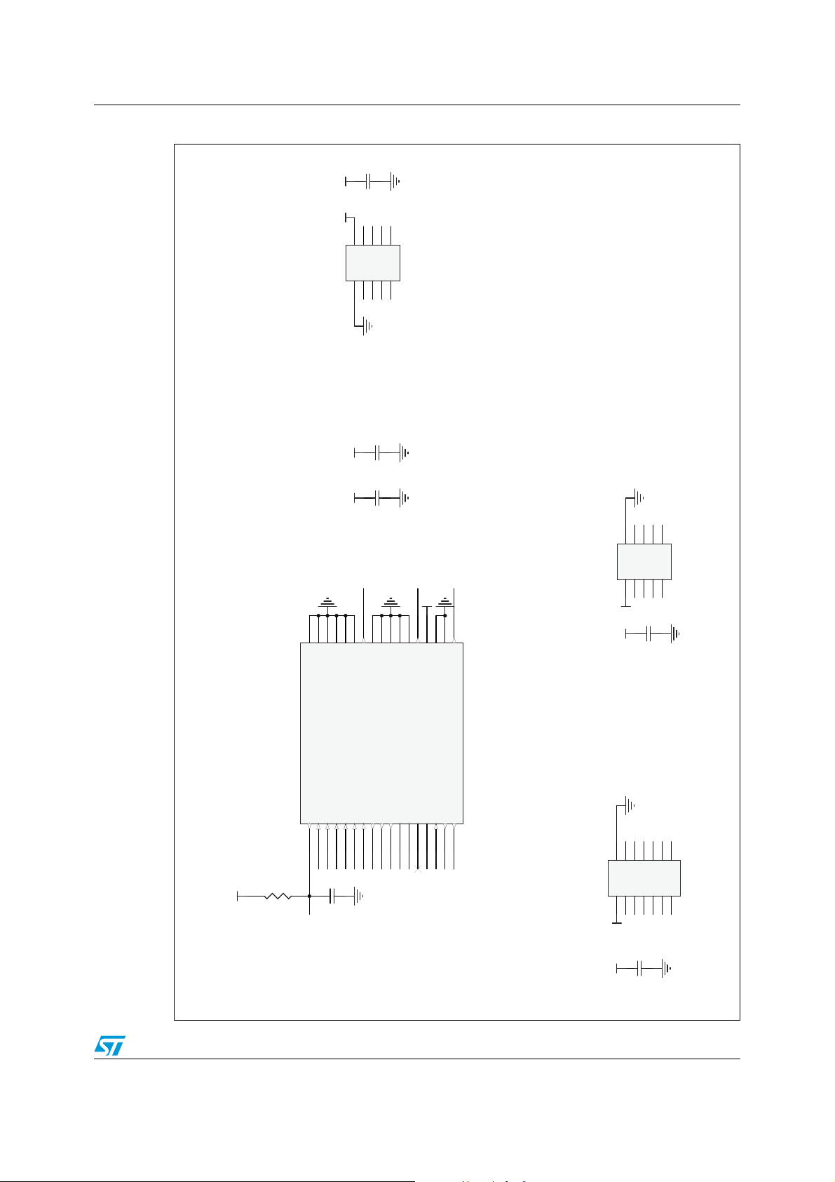
Demonstration board schematic STEVAL-IFW001V1
Figure 5. MCU
C46
100nF
C45
3V3
C44
C43
C42
C41
C40
C39
LK
100nF
100nF
100nF
100nF
100nF
100nF
100nF
4
3
DC
L
_CL K
_C
C50
100nF
C49
100nF
1V8
C48
100nF
C47
100nF
JTRST
JTCK
JTMS
JTDI
JTDO
JRTCK
RTC_X2
RTC_X1
RTC- X241RTC- X1
42
EMI _AL E74EMI _RD
MI I_MDI O
91
96
95
94
USB-
USB+
5
MI I_MDI O
RTC_TAMP ER1
6
1
6
5
4
2
1
7
6
3
1
0
3
2
EMI _WR/WRL
EMI _WRH
21
22
75
U4A
STR912F W44X6
97
107
111
117
108
115
TDI
TCK
TMS
TRST
104
MCU_X2
MCU_X1
103
TDO
100
RTCK
RESET_I N89RESET_OUT
P47
P46
5
P4
P44
P43
P42
P41
P40
7
P3
P36
P35
P34
3
P3
32
P
P31
P30
SPI_P27
SPI_P26
SPI_P25
SPI_P2
I2C_P2
I2
C_P22
P21
P20
M
M
II_
M
II_CRS
M
II_CO
TXD3
MII_
TXD2
MII_
MII_TXD1
MII_TXD0
MII_RX_ER
M
II_RX_DV
M
II_RX
MII_RXD3
MII_RXD2
M
RXD1
II_
MII
RXD0
_
P01
TX
MII_
P46
125
45
P
126
P44
127
P43
128
P42
1
P41
2
P40
3
P37
8
6
P36
6
6
P35
65
P34
3
6
P33
1
6
P32
0
6
1
P3
9
5
P30
5
5
P27
54
6
P2
3
5
25
P
5
4
P24
7
3
P23
5
3
P22
3
3
P21
1
1
P20
0
1
P17
116
P16
14
1
P15
110
P14
109
P13
0
1
6
P12
01
1
11
P
9
9
P10
8
9
P07
0
9
P06
8
8
P05
85
P04
8
7
3
P0
6
7
02
P
1
7
P01
9
6
P00
7
6
P47
124
3V3
102
43
23
86
VCCQ9VCCQ
VCCQ57VCCQ73VCCQ
VCCQ(RTC)
VSS16VSS48VSS82VSS
U4B
113
81
1V8
P97
64
P96
P9
P94
P93
P92
P91
P90
P87
P
8
P85
P84
P83
P82
P8
P80
P77
P
7
P
7
P
7
P73
P
7
P7
P70
P
6
P6
P65
P64
P
6
P62
P
6
P
6
P57
P56
P55
P54
P
5
P5
P51
P50
P97
62
P96
5
8
P95
52
P94
51
93
P
50
P92
47
P91
4
P90
6
44
P87
3
8
86
P
36
P85
8
4
P
3
4
P83
32
3
P82
0
2
81
8
P
8
2
0
6
P
11
P77
9
76
P
118
7
1
5
5
P
1
P74
4
1
3
P73
7
P72
71
6
P
P70
5
9
3
P67
9
2
P66
6
8
5
4
P
83
P64
2
P63
0
6
1
2
P
9
61
3
P
1
P60
29
P57
8
0
7
P56
9
77
P55
5
7
P
0
4
2
EN
7
2
5
1
8
0
1
2
P5
EMI_P97
EMI_P96
EMI_P95
EMI_P94
EMI_P9
3
EMI_P92
9
1
EMI_P
EM
P90
I_
EMI_P87
EMI_P86
EMI_P85
EMI_P8
4
EMI_P8
3
EMI_P82
E
P8
MI_
1
EMI_P8
0
EMI_P77
EMI_P7
6
_P7
EM
I
5
_P7
EM
I
4
EMI_P73
EMI_P72
EM
_P7
I
1
EMI_P70
MDINT_2
EMI_P54
II_TX_
M
PHY_CLK
UART_P51
P51
A
P50
U
RT_
40
105
24
87
VSSQ56VSSQ72VSSQ
VSSQ(RTC)
AGND4VBAT
AVDD
122
8pF
RTC_X1
MCU_X1
8pF
121
VSSQ
VSSQ(P CL L )
39
3V3
32
41
MC- 146
X1
32K Hz
R56
1M
X2
25MHz
32
41
STR912F W44X6
C55
C54
8pF
RTC_X2
MCU_X2
8pF
120
VSSQ8VSSQ
VCCQ
VCCQ(P L L )
VDD17VDD49VDD
AVREF
VDD
123
112
3V3AN
C53
C52
CM5032
B2
M
II_
MII_MDINT_1
R55
10K
3V3
GM: P-DT2112C
RESET_I N
2
1
C51
100nF
RESET_I N
MCU_X1
MCU_X2
RESET_OUT
EMI _AL E
EMI _RD
EMI _WRH
EMI _WR/WRL
6/9

STEVAL-IFW001V1 Demonstration board schematic
Figure 6. Power supply
LD4
Red
2.0V
LD3
Red
3V3
C59
R57
R59
10V
Tantal
100uF
220
5K 6
(C,D,E)
12
R58
3K 3
2.0V
1V8
1V83V3
R6
C58
C64
100
10nF
2.2uF
12
DO3316P-333
PW1 ST:L 5973D
1
6
Vin
5
OUT
VREF
8
3A, 40VD1
L 3 33uH
FB
SYNC
VCC
2
C60
D
4
35V
N
G
GND
NH
I
COMP
10uF
Ceramic
STP S340U
9
7
3
(C,D,E)
C62
22nF
C63
220pF
Vin
R60
4k7
D3
ST:SM6T33A
PW2
L F18xDT
Max.16V Max.500mA
2
1
Vout
ND
Vin
G
C56
Tantal
(A,B)
3
100nF
C57
10nF
Vin
CN7
3A, 40V
132
D2 ST:STP S340U
L 4 3.3uH
3V3 3V3AN
GM: K 375A
1
2
MK DS1.5- 5.08 or GM: ARK103/2
CN5
C61
10uF
Tantal
(A,B)
0603PS-332K LC
7/9

Revision history STEVAL-IFW001V1
2 Revision history
Table 1. Document revision history
Date Revision Changes
01-Sep-2008 1 Initial release.
8/9

STEVAL-IFW001V1
Please Read Carefully:
Information in this document is provided solely in connection with ST products. STMicroelectronics NV and its subsidiaries (“ST”) reserve the
right to make changes, corrections, modifications or improvements, to this document, and the products and services described herein at any
time, without notice.
All ST products are sold pursuant to ST’s terms and conditions of sale.
Purchasers are solely responsible for the choice, selection and use of the ST products and services described herein, and ST assumes no
liability whatsoever relating to the choice, selection or use of the ST products and services described herein.
No license, express or implied, by estoppel or otherwise, to any intellectual property rights is granted under this document. If any part of this
document refers to any third party products or services it shall not be deemed a license grant by ST for the use of such third party products
or services, or any intellectual property contained therein or considered as a warranty covering the use in any manner whatsoever of such
third party products or services or any intellectual property contained therein.
UNLESS OTHERWISE SET FORTH IN ST’S TERMS AND CONDITIONS OF SALE ST DISCLAIMS ANY EXPRESS OR IMPLIED
WARRANTY WITH RESPECT TO THE USE AND/OR SALE OF ST PRODUCTS INCLUDING WITHOUT LIMITATION IMPLIED
WARRANTIES OF MERCHANTABILITY, FITNESS FOR A PARTICULAR PURPOSE (AND THEIR EQUIVALENTS UNDER THE LAWS
OF ANY JURISDICTION), OR INFRINGEMENT OF ANY PATENT, COPYRIGHT OR OTHER INTELLECTUAL PROPERTY RIGHT.
UNLESS EXPRESSLY APPROVED IN WRITING BY AN AUTHORIZED ST REPRESENTATIVE, ST PRODUCTS ARE NOT
RECOMMENDED, AUTHORIZED OR WARRANTED FOR USE IN MILITARY, AIR CRAFT, SPACE, LIFE SAVING, OR LIFE SUSTAINING
APPLICATIONS, NOR IN PRODUCTS OR SYSTEMS WHERE FAILURE OR MALFUNCTION MAY RESULT IN PERSONAL INJURY,
DEATH, OR SEVERE PROPERTY OR ENVIRONMENTAL DAMAGE. ST PRODUCTS WHICH ARE NOT SPECIFIED AS "AUTOMOTIVE
GRADE" MAY ONLY BE USED IN AUTOMOTIVE APPLICATIONS AT USER’S OWN RISK.
Resale of ST products with provisions different from the statements and/or technical features set forth in this document shall immediately void
any warranty granted by ST for the ST product or service described herein and shall not create or extend in any manner whatsoever, any
liability of ST.
ST and the ST logo are trademarks or registered trademarks of ST in various countries.
Information in this document supersedes and replaces all information previously supplied.
The ST logo is a registered trademark of STMicroelectronics. All other names are the property of their respective owners.
© 2008 STMicroelectronics - All rights reserved
STMicroelectronics group of companies
Australia - Belgium - Brazil - Canada - China - Czech Republic - Finland - France - Germany - Hong Kong - India - Israel - Italy - Japan -
Malaysia - Malta - Morocco - Singapore - Spain - Sweden - Switzerland - United Kingdom - United States of America
www.st.com
9/9
 Loading...