16-bit PLC digital input card demonstration board
Features
■ 8/16 input channel topology (SCLT3-8
chip/STEVAL-IFP007V1 board)
■ Fully integrated current limiter
■ Termination for IEC61131-2 type 1 and 3
inputs
■ Digital filter in each input
■ SPI communication peripheral
■ Voltage regulator integrated on the chip
■ Thermal alarm
■ Wide range supply voltage operation
STEVAL-IFP007V1
based on the SCLT3
Data brief
Description
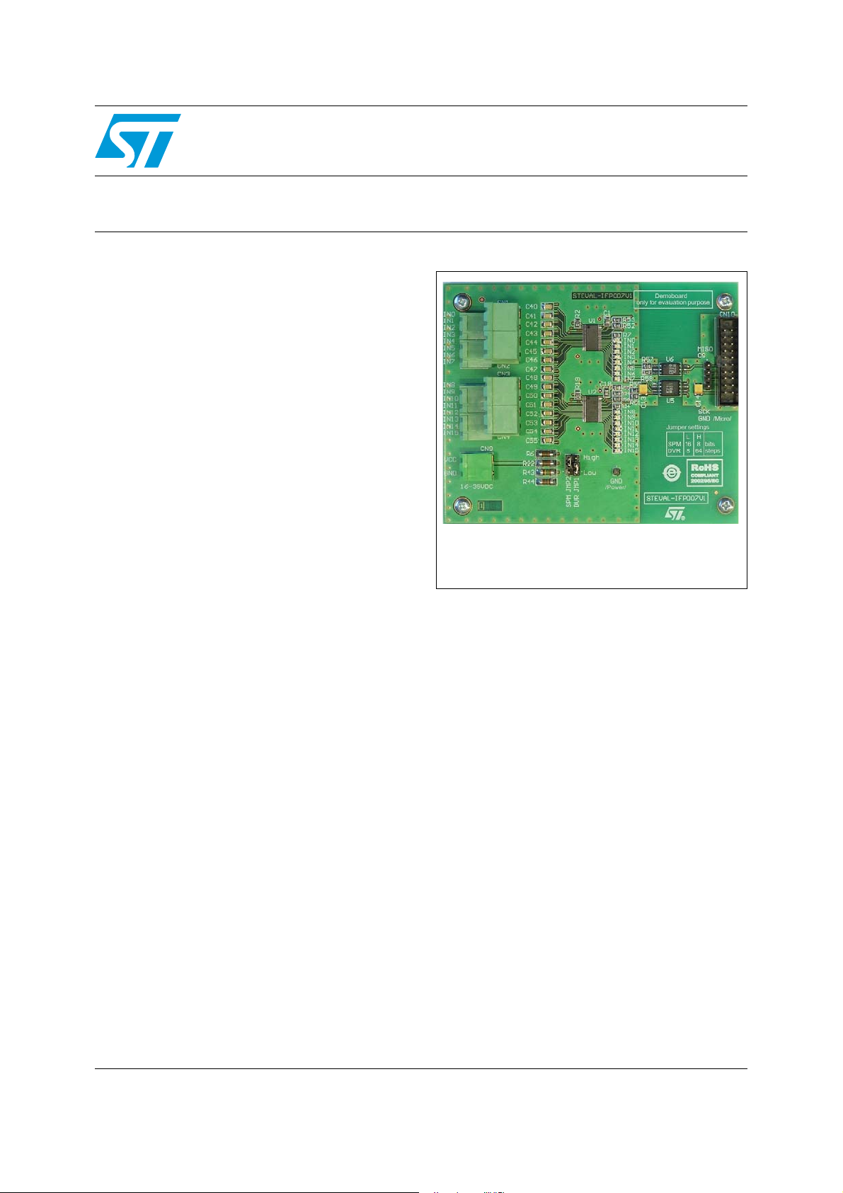
The STEVAL-IFP07V1 demonstration board is
based on the SCLT3-8 protected digital input
termination with serialized state transfer, and
allows the user to evaluate the behavior of the
SCLT3-8 device in industrial environmental
conditions.
The SCLT3-8 is an eight channel termination
used to interface automation digital inputs. It is
designed for 24 VDC applications, and supports
the type 3 input characteristic in accordance with
standard IEC61131-2 (programmable controllers).
The device integrates an SPI peripheral for
communication with logic devices, ASICs and
microcontrollers.
This demonstration board is capable of
transferring not only the data but also additional
information such as thermal alarms, under
voltage indications and parity bits. The STEVALIFP07V1 is ideal for applications with a high
channel count, while the serial communication
reduces the number of lines which, in most final
applications, require galvanic isolation.
STEVAL-IFP007V1
interface and indicates each sensor logic state
with an LED.
The board accommodates two SCLT3-8 chips
connected to the SPI bus in a "daisy-chain"
configuration. It offers a 16-bit digital input
May 2009 Doc ID 15371 Rev 2 1/4
For further information contact your local STMicroelectronics sales office.
www.st.com
4

Circuit schematic STEVAL-IFP007V1
CN
ST70
2x2
CN
ST70
2x2
CN
ST70
2x2
CN
ST70
2x2
2k2
2k2
2k2
2k2
2k2
2k2
R1
2k2
R1
2k2
R1
2k2
R1
2k2
R1
2k2
R1
2k2
R1
2k2
R1
2k2
R1
2k2
R2
2k2
R2
SGN
GN
CR
GN
CRO_VC
CR
GN
SO_u
_u
nCS_u
_MASTER
to
be
connected
_S
AV
nput
nput
nput
nput
nput
nput
nput
nput
nput
nput
nput
10
nput
11
nput
12
nput
13
nput
14
nput
15
GN
N1
N1
N1
N1
N1
N1
N1
N1
N1
N1
N1
N1
DV
51k
SGN
1k0
SGN
nCS_SC
SC
_S
SD_
15k
ED
ED
ED
ED
ED
ED
ED
ED
51kR1R1
SGN
1k0R2R2
SGN
DV
R4
120kR4R4
SGN
SGN
SO_SC
15k
R2
ED
ED
SD_0f
GN
SGN
VC
VC
VC
DV
JM
JM
VDD
SGN
SGN
VDD
SGN
VD
SGN
VD
CR
GN
33n
33n
33n
100n
11
12
13
14
15
16
17
18
19
20
CN1
W20
SC
Test
poin
_u
Test
poin
nCS_u
Test
poin
SO_u
GND_MI
CR
Test
poin
CR
GN
GND_
Test
poin
GN
10u
/6.3V
C1
10u
/6.3V
C1
VD
SGN
330R
R4
nCS_u
_u
CRO_VC
22
R5
SGN
VD
33n
C1
22
R5
100p
C1
SC
_O
220R
R5
SC
_S
100p
C2
nCS_O
220R
R5
nCS_SC
SC
_O
220R
R5
SC
_S
100p
C2
nCS_O
220R
R5
nCS_SC
nCS_SC
SC
_S
100p
C2
220R
R5
SD_
SD_0f
330R
R5
CRO_VC
100n
C2
VDD
SGN
SGN
SGN
SGN
SGN
1n
C4
1n
C4
1n
C4
1n
C4
1n
C4
1n
C4
1n
C4
1n
C4
1n
C4
1n
C4
1n
C5
1n
C5
1n
C5
1n
C5
1n
C5
1n
C5
GN
CN
ST04
2pin
330R
R5
330R
R4
330R
R6
CR
GN
SO_u
330R
R5
SGN
SO_SC
SC
_O
nCS_O
Shi
73
Shi
GN
VD
W70
solation
barrie
VC
COM
DV
OS
VD
38
10
11
13
14
15
16
COM
12
COM
17
35
20
21
22
23
24
25
26
27
RE
29
COMs
30
31
32
MOS
33
SC
34
COM
18
19
28
36
37
SC
8BT
VC
COM
DV
OS
VD
38
10
11
13
14
15
16
COM
12
COM
17
35
20
21
22
23
24
25
26
27
RE
29
COMs
30
31
32
MOS
33
SC
34
COM
18
19
28
36
37
SC
8BT
VC_U
VC_U
100p
C2
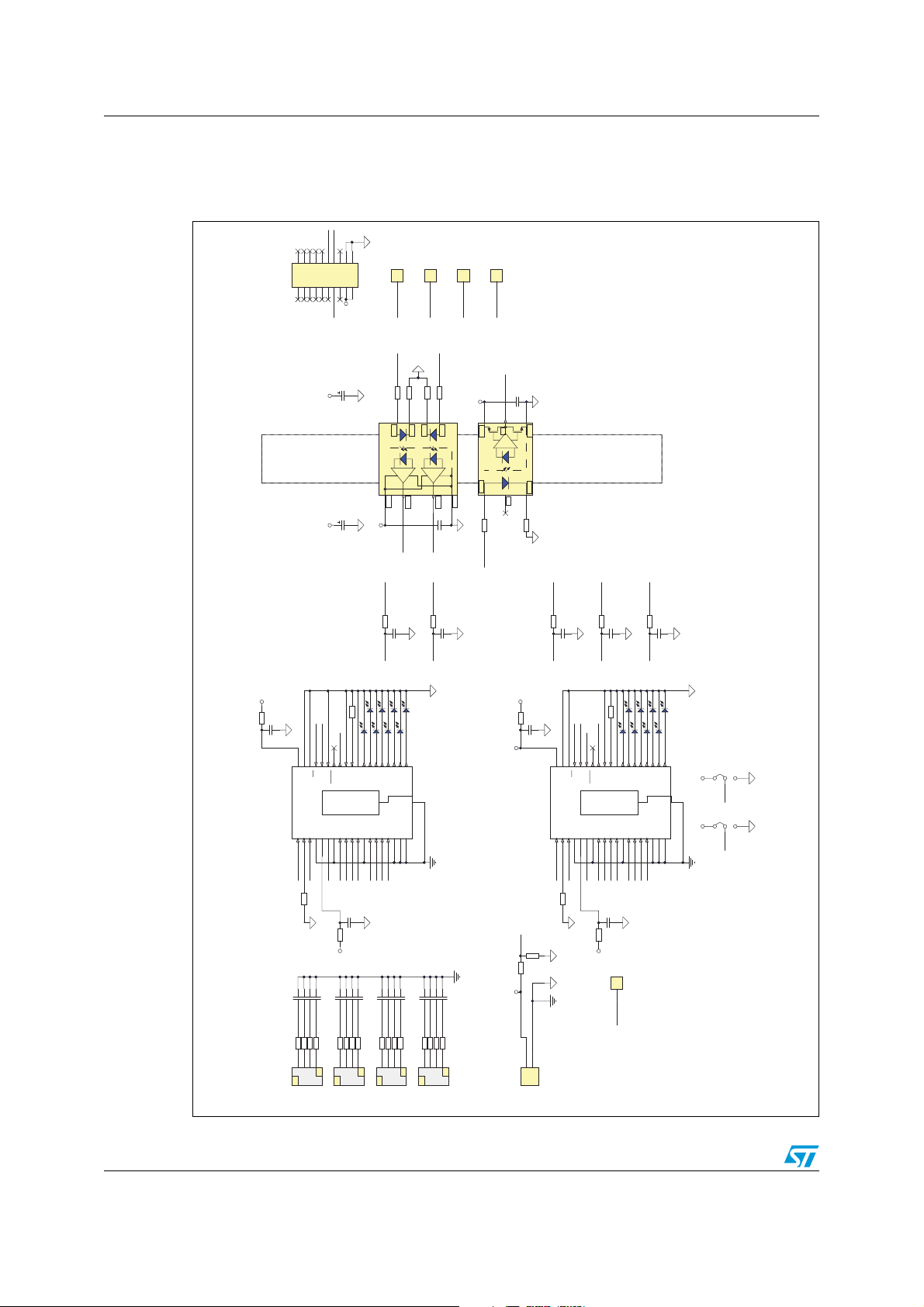
1 Circuit schematic
Figure 1. Schematic diagram
D
C
C
connected
be
to
SPI_MASTER
2/4 Doc ID 15371 Rev 2
D
VD
RR5
F
22
0
33n
C1
LSBSPI_S
E
LAV
CL K_u
0
1 2
3 4
5 6
7 8
9 101011
CN1
C
MICRO_VC
D
VD
D
L T1
CL T1
SGN
K _S
nCS_SC
SC
35
38
34
36
37
33
K
D
CS
NC
NC
SC
VD
p
R
C
DV
OS
SPM3VC
COM
U1
1
2
6
5
4
1
R
S
DV
SPM
VC
VC_U
51k
R2
D
SGN
FC4
FC4
FC4
FC4
1n
1n
1n
1n
0
3
2
1
IN0
IN1
IN2
IN3
2k2
2k2
2k2
2k2
R1
R3
R4
R5
123
2x2
1
4
ST70
CN
0
1
2
3
Input
Input
Input
Input
O_GN
MISO_u
MICR
t
t
t
t
G
poin
C
CL K_u
C
CL K_u
132
A1
9
C1
LD6
p
p
COM
10
Input
1
7
PT
K _O
SC
F
100p
6
LED
21
LD7
M
NC
18
FC5
1n
1
1
IN1
2k2
6
R1
4
11
Input
Test
D
O_GN
MICR
330R
9
R5
C1
Vo1Vo
D
SGN
7
LED
20
8
LD8
L T3-8BT
SC
C
O
9
NC
19
2x2
4
ST70
CN
poin
1
CS
Test
C
nCS_u
C
nCS_u
330R
330R
9
0
R4
R6
4
C2
2
6
C2
PT
nCS_O
PT
nCS_O
220R
3
R5
L T1
nCS_SC
DGN
SGN
3
D
FC5
FC5
FC5
FC5
1n
1n
1n
1n
2
3
4
5
2
3
4
5
IN1
IN1
IN1
IN1
2k2
2k2
2k2
2k2
7
8
0
1
R1
R1
R2
R2
123
12
13
14
Input
Input
Input
12
14
16
18
20
K
17
C
MICRO_VC
F/6.3V
10u
F/6.3V
10u
30
COMs
IN29IN3
IN1
1k0
FC4
1n
5
IN5
2k2
0
R1
5
Input
SC
19
ML W20
D
330R
O_GN
8
R4
MICR
U5
D
8
VD
D
D
VD
SGN
PT
K _O
SC
220R
2
R5
CL T1
K _S
SC
15k
1
3
5
R7
LED
LED
LED
0
2
4
LED
LED
LED
29
28
22
23
24
25
26
27
F
NC
LD5
LD4
LD3
LD2
LD1
RE
p
IN4
IN5
IN6
IN7
IN8
COM
12
17
10
11
13
14
15
16
IN2
IN3
IN4
IN5
IN6
IN7
F
33n
C4
D
SGN
FC4
FC4
FC4
FC4
FC5
1n
1n
1n
1n
1n
6
7
8
9
0
0
IN6
IN7
IN8
IN9
IN1
2k2
2k2
2k2
2k2
2k2
1
2
3
4
5
R1
R1
R1
R1
R1
123
2x2
3
4
ST70
CN
6
7
8
9
Input
Input
Input
Input
13
15
C
nCS_u
4
C1
3
C1
0
SD_
31
32
I
MISO
MISO
MOS
p
S
VC
COM
IN1
8
7
IN0
R6
VCC
FC4
1n
4
IN4
2k2
R8
123
2
CN
4
Input
O
CR
poin
poin
1
1
MISO
A2
eld
Shi
D
5
GN
F
100n
F
0
C2
100p
2x2
4
ST70
15
Input
Test
Test
GND_MI
D
C
O_GN
MISO_u
MICR
C
F
5
C
MICRO_VC
61
L
D
VD
ACP L-K 73
A
U6
D
330R
7
SGN
R5
L T
MISO_SC
D
SGN
D
GN
D
MISO_u
100n
C2
O_GN
MICR
4
5
L
D
Vo
GN
ACP L-W70
eld
Shi
C
3
2
NC
330R
8
D
R5
SGN
PT
K _O
SC
220R
4
R5
CL T2
K _S
SC
D
VD
RR5
F
22
8
1
33n
C1
4
VDD
U2
S
VC
4
120k
3
1M5
R4
VCC
2
1
2pin
9
ST04
CN
PT
nCS_O
L T2
nCS_SC
35
CS
p
COM
4
F
220R
2
C2
5
100p
D
R5
SGN
L T2
nCS_SC
15k
4
R2
L T
CL T2
8
K _S
SD_0f
MISO_SC
LED
SC
31
32
29
34
30
28
33
27
I
F
K
NC
RE
SC
MISO
MISO
MOS
COMs
p
S
VC
COM
IN1
IN29IN3
IN4
7
6
8
5
12
10
11
2
0
1
S
VC_U
IN8
IN9
IN1
VC
IN1
F
33n
C6
D
SGN
2
1k0
VCC
P WR
1
GND_
D
GN
F
1
C2
100p
D
SGN
38
36
37
D
NC
NC
VD
R
C
DV
OS
SPM3VC
1
2
R
DV
SPM
9
51k
D
SGN
D
D SGN
GN
r
barrie
Isolation
0SD_0f
SD_
F
220R
3
C2
6
100p
D
SGN
9
LED
LED10
25
26
LD3
LD2
LD1
p
IN5
IN6
COM
13
14
2
3
IN1
IN1
D
SGN
t
poin
Test
D
R5
SGN
D
SGN
LED11
LED13
LED15
LED12
LED14
20
21
22
23
24
LD8
LD7
LD6
LD5
LD4
COM p
p
IN7
IN8
COM
NC
NC
17
15
16
18
19
4
5
IN1
IN1
P2
8
4
VDD
L T3-8BT
SC
39
4
VDD
D
GN
D
P1 JM
D SGN
SGN
R SPMJM
DV

STEVAL-IFP007V1 Revision history
2 Revision history
Table 1. Document revision history
Date Revision Changes
17-Feb-2009 1 Initial release.
05-May-2009 2 Updated picture on cover page and schematic diagram (Figure 1)
Doc ID 15371 Rev 2 3/4

STEVAL-IFP007V1
Please Read Carefully:
Information in this document is provided solely in connection with ST products. STMicroelectronics NV and its subsidiaries (“ST”) reserve the
right to make changes, corrections, modifications or improvements, to this document, and the products and services described herein at any
time, without notice.
All ST products are sold pursuant to ST’s terms and conditions of sale.
Purchasers are solely responsible for the choice, selection and use of the ST products and services described herein, and ST assumes no
liability whatsoever relating to the choice, selection or use of the ST products and services described herein.
No license, express or implied, by estoppel or otherwise, to any intellectual property rights is granted under this document. If any part of this
document refers to any third party products or services it shall not be deemed a license grant by ST for the use of such third party products
or services, or any intellectual property contained therein or considered as a warranty covering the use in any manner whatsoever of such
third party products or services or any intellectual property contained therein.
UNLESS OTHERWISE SET FORTH IN ST’S TERMS AND CONDITIONS OF SALE ST DISCLAIMS ANY EXPRESS OR IMPLIED
WARRANTY WITH RESPECT TO THE USE AND/OR SALE OF ST PRODUCTS INCLUDING WITHOUT LIMITATION IMPLIED
WARRANTIES OF MERCHANTABILITY, FITNESS FOR A PARTICULAR PURPOSE (AND THEIR EQUIVALENTS UNDER THE LAWS
OF ANY JURISDICTION), OR INFRINGEMENT OF ANY PATENT, COPYRIGHT OR OTHER INTELLECTUAL PROPERTY RIGHT.
UNLESS EXPRESSLY APPROVED IN WRITING BY AN AUTHORIZED ST REPRESENTATIVE, ST PRODUCTS ARE NOT
RECOMMENDED, AUTHORIZED OR WARRANTED FOR USE IN MILITARY, AIR CRAFT, SPACE, LIFE SAVING, OR LIFE SUSTAINING
APPLICATIONS, NOR IN PRODUCTS OR SYSTEMS WHERE FAILURE OR MALFUNCTION MAY RESULT IN PERSONAL INJURY,
DEATH, OR SEVERE PROPERTY OR ENVIRONMENTAL DAMAGE. ST PRODUCTS WHICH ARE NOT SPECIFIED AS "AUTOMOTIVE
GRADE" MAY ONLY BE USED IN AUTOMOTIVE APPLICATIONS AT USER’S OWN RISK.
Resale of ST products with provisions different from the statements and/or technical features set forth in this document shall immediately void
any warranty granted by ST for the ST product or service described herein and shall not create or extend in any manner whatsoever, any
liability of ST.
ST and the ST logo are trademarks or registered trademarks of ST in various countries.
Information in this document supersedes and replaces all information previously supplied.
The ST logo is a registered trademark of STMicroelectronics. All other names are the property of their respective owners.
© 2009 STMicroelectronics - All rights reserved
Australia - Belgium - Brazil - Canada - China - Czech Republic - Finland - France - Germany - Hong Kong - India - Israel - Italy - Japan -
STMicroelectronics group of companies
Malaysia - Malta - Morocco - Philippines - Singapore - Spain - Sweden - Switzerland - United Kingdom - United States of America
www.st.com
4/4 Doc ID 15371 Rev 2
 Loading...