Quad high side smart power solid state relay evaluation board
Features
■ Shorted load protections
■ Junction over-temperature protection
■ Case over-temperature protection for thermal
independence of the channels
■ Thermal case shut-down non-simultaneous
restart for the various channels
■ Protection against loss of ground
■ Current limitation
■ Undervoltage shut-down
■ Open drain diagnostic outputs
■ 3.3 V CMOS/TTL compatible inputs
■ Fast demagnetization of inductive loads
■ Conforms to IEC 61131-2
STEVAL-IFP006V1
using the VNI4140K
Data Brief
STEVAL-IFP006V1
Description
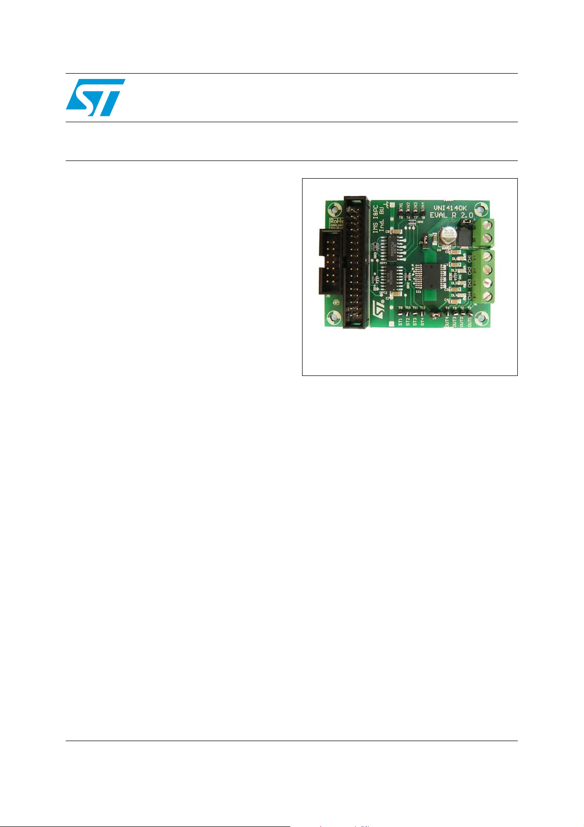
The purpose of this design is to demonstrate the
features of the VNI4140K quad high side smart
power solid state relay. The application offers
robustness and complies with EMC industrial
standards. It implements short-circuit/overload
protection and thermal management as well,
achieving best-in-class MTBF values. The
reference design is suitable for use in
programmable logic controllers (PLCs) as well as
to drive generic loads which require up to 0.7 A of
nominal current (the typical current limitation is
0.7 - 1.7 A). Thanks to the very low R
80 mΩ typ. @ 25 °C per channel) the device
allows very low power consumption during
operation and for this reason making it an ideal
solution for IP65 / IP67 requirements. The device
is compliant with IEC 61131-2 (Programmable
Controllers International Standard).
DS(on)
(only
December 2007 Rev 1 1/8
For further information contact your local STMicroelectronics sales office.
www.st.com
8

Board schematic STEVAL-IFP006V1
1 Board schematic
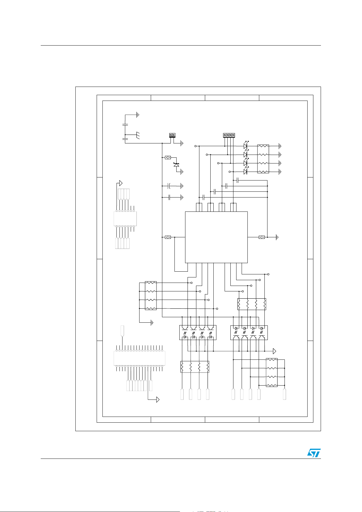
Figure 1. Schematic diagram
B
OUT4
OUT3
OUT1
OUT2
M1
M.4VITEB
123
4
T3
T4
C3
10nF LV
1206
10nF LV
1206
13
STAT1
STAT37STAT4
STAT2
3
9
5
1206
GND
VNI4140K
DL1
DL2
DL3
DL4
6
LED
LED
LED
LED
10nF LV
RR1
C4
10K 1206
J3
GND DISC. TEST
A B
T11
T10
T9
OPEN
+
J2
FOR
J4
GND
+24Vdc
1
2
A B
OVL TEST
C6
C5
Vcc DISC. TEST
A B
47uF
100nF
OR
C
M2
M.2VITEB
D1
SM15T39AC
1206
IC1
CURRENT PROBE
Vcc
TAB
Vcc
1
T1
OUT1_a24OUT1_b23OUT1_c22OUT2_a
IN1
2
T2
C1
10nF LV
21
IN2
4
C2
1206
20
OUT2_b
OUT2_c19OUT3_a18OUT3_b17OUT3_c16OUT4_a15OUT4_b14OUT4_c
VNI4140K
IN38IN4
10
D
C8
4.7nF
4
321
1 2
VDD
C7
4.7nF
STAT4STAT3
STAT2STAT1
3 4
5 6
7 8
9 10
11 12
13 14
J5
CAN7
IN1 IN2
IN3 IN4
RR5
47K 1206
T5
T6
A
T12
T7
RR2
T8
10111213141516
89
10K 1206
1234567
STAT1
1 2
3 4
5 6
7 8
9 10
11 12
13 14
15 16
17 18
19 20
21 22
23 24
25 26
27 28
29 30
31 32
33 34
J1
EVALCOMMBOARD
IN1
IN2
IN3
IN4
VDD
STAT4
STAT3
STAT2
D
2/8
1234567
IN1
IN2
IN3
C
OPT1
TLP281-4
8 9
RR3
IN4
1K 1206
10111213141516
STAT1
STAT2
STAT3
B
STAT4
OPT2
TLP281-4
1 2 34
VDD
RR4
10K 1206
A

STEVAL-IFP006V1 Connectors
2 Connectors
This evaluation board uses two input header connectors, one screw drives the four-channels
output connector and one screw drives the two-channel supply connector.
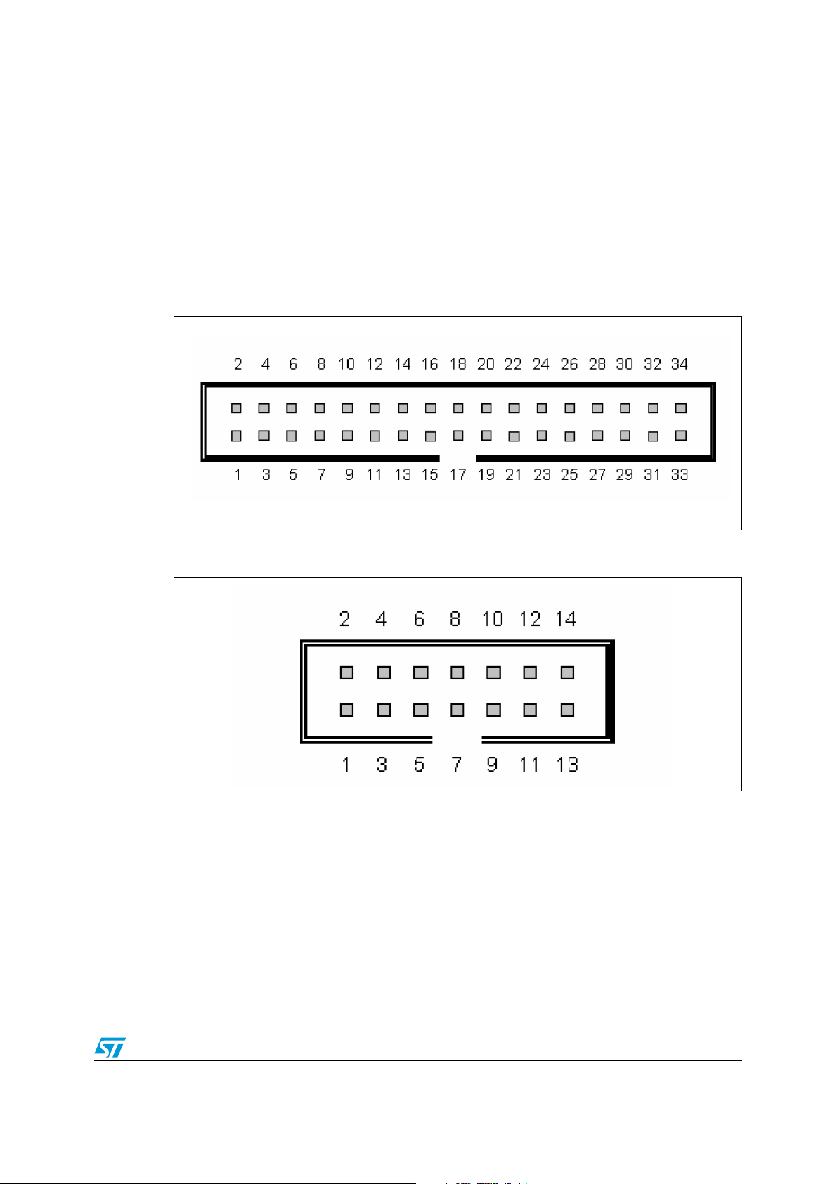
Both input connectors, J5 and J1, provide the same bidirectional evaluation board
signalization guaranteeing the maximum compatibility with existing ST tools, such as the
ST7540 FSK powerline transceiver evaluation board (see AN2451 ) and similar.
Figure 2. J1 connector pinout
Figure 3. J5 connector pinout
3/8

Connectors STEVAL-IFP006V1
Table 1. Connector J1 and J5 pinout mapping
J1 pin number J5 pin number Signal Type
11 1 Vdd 5/3.3 V supply voltage
23 2 GND Signal ground
9 3 IN1 Input channel 1
13 4 IN2 Input channel 2
15 5 IN3 Input channel 3
17 6 IN4 Input channel 4
6 7 STAT1 Status channel 1
25 8 STAT2 Status channel 2
21 9 STAT3 Status channel 3
19 10 STAT4 Status channel 4
4/8

STEVAL-IFP006V1 Bill of materials
3 Bill of materials
Table 2. Evaluation board bill of material
Designator Part Description
RR1 10 kΩ x 4 SMD resistor pack 1206 format
RR2 10 kΩ x 4 SMD resistor pack 1206 format
RR3 1 kΩ x 4 SMD resistor pack 1206 format
RR4 10 kΩ x 4 SMD resistor pack 1206 format
RR5 47 kΩ x 4 SMD resistor pack 1206 format
C1 10 nF LV SMD capacitor 1206 format
C2 10 nF LV SMD capacitor 1206 format
C3 10 nF LV SMD capacitor 1206 format
C4 10 nF LV SMD capacitor 1206 format
C5 100 nF SMD capacitor 1206 format
C6 47 µF 50 V SMD electrolitic capacitor
C7 4.7 nF SMD capacitor 1206 format
C8 4.7 nF SMD capacitor 1206 format
D1 SM15T39AC Transil diode
DL1 LED SMD LED diode 0805 format
DL2 LED SMD LED diode 0805 format
DL3 LED SMD LED diode 0805 format
DL4 LED SMD LED diode 0805 format
OPT1 PC3Q66Q 4 channel opto isolator
OPT2 PC3Q66Q 4 channel opto isolator
IC1 VNI4140K ST IC industrial 4 ch hsd
J1 Hader 34 pin Compatible evalcommboard
J2 Jumper Over voltage test
J3 Jumper Ground disconnection test
J4 Jumper Vcc disconnection test
J5 HADER 14 pin Compatible ST7CANIC DB
M1 4 screw plug HSD output connector
M2 2 screw plug Power supply conector
T1 Test point HSD output channel 1 voltage
T2 Test point HSD output channel 2 voltage
T3 Test point HSD output channel 3 voltage
T4 Test point HSD output channel 4 voltage
5/8

Bill of materials STEVAL-IFP006V1
Table 2. Evaluation board bill of material (continued)
T5 Test point HSD input channel 1 signal
T6 Test point HSD input channel 2 signal
T7 Test point HSD input channel 3 signal
T8 Test point HSD input channel 4 signal
T9 Test point HSD channel 1 status
T10 Test point HSD channel 2 status
T11 Test point HSD channel 3 status
T12 Test point HSD channel 4 status
6/8

STEVAL-IFP006V1 Revision history
4 Revision history
Table 3. Document revision history
Date Revision Changes
13-Dec-2007 1 Initial release
7/8

STEVAL-IFP006V1
Please Read Carefully:
Information in this document is provided solely in connection with ST products. STMicroelectronics NV and its subsidiaries (“ST”) reserve the
right to make changes, corrections, modifications or improvements, to this document, and the products and services described herein at any
time, without notice.
All ST products are sold pursuant to ST’s terms and conditions of sale.
Purchasers are solely responsible for the choice, selection and use of the ST products and services described herein, and ST assumes no
liability whatsoever relating to the choice, selection or use of the ST products and services described herein.
No license, express or implied, by estoppel or otherwise, to any intellectual property rights is granted under this document. If any part of this
document refers to any third party products or services it shall not be deemed a license grant by ST for the use of such third party products
or services, or any intellectual property contained therein or considered as a warranty covering the use in any manner whatsoever of such
third party products or services or any intellectual property contained therein.
UNLESS OTHERWISE SET FORTH IN ST’S TERMS AND CONDITIONS OF SALE ST DISCLAIMS ANY EXPRESS OR IMPLIED
WARRANTY WITH RESPECT TO THE USE AND/OR SALE OF ST PRODUCTS INCLUDING WITHOUT LIMITATION IMPLIED
WARRANTIES OF MERCHANTABILITY, FITNESS FOR A PARTICULAR PURPOSE (AND THEIR EQUIVALENTS UNDER THE LAWS
OF ANY JURISDICTION), OR INFRINGEMENT OF ANY PATENT, COPYRIGHT OR OTHER INTELLECTUAL PROPERTY RIGHT.
UNLESS EXPRESSLY APPROVED IN WRITING BY AN AUTHORIZED ST REPRESENTATIVE, ST PRODUCTS ARE NOT
RECOMMENDED, AUTHORIZED OR WARRANTED FOR USE IN MILITARY, AIR CRAFT, SPACE, LIFE SAVING, OR LIFE SUSTAINING
APPLICATIONS, NOR IN PRODUCTS OR SYSTEMS WHERE FAILURE OR MALFUNCTION MAY RESULT IN PERSONAL INJURY,
DEATH, OR SEVERE PROPERTY OR ENVIRONMENTAL DAMAGE. ST PRODUCTS WHICH ARE NOT SPECIFIED AS "AUTOMOTIVE
GRADE" MAY ONLY BE USED IN AUTOMOTIVE APPLICATIONS AT USER’S OWN RISK.
Resale of ST products with provisions different from the statements and/or technical features set forth in this document shall immediately void
any warranty granted by ST for the ST product or service described herein and shall not create or extend in any manner whatsoever, any
liability of ST.
ST and the ST logo are trademarks or registered trademarks of ST in various countries.
Information in this document supersedes and replaces all information previously supplied.
The ST logo is a registered trademark of STMicroelectronics. All other names are the property of their respective owners.
© 2007 STMicroelectronics - All rights reserved
STMicroelectronics group of companies
Australia - Belgium - Brazil - Canada - China - Czech Republic - Finland - France - Germany - Hong Kong - India - Israel - Italy - Japan -
Malaysia - Malta - Morocco - Singapore - Spain - Sweden - Switzerland - United Kingdom - United States of America
www.st.com
8/8
 Loading...