

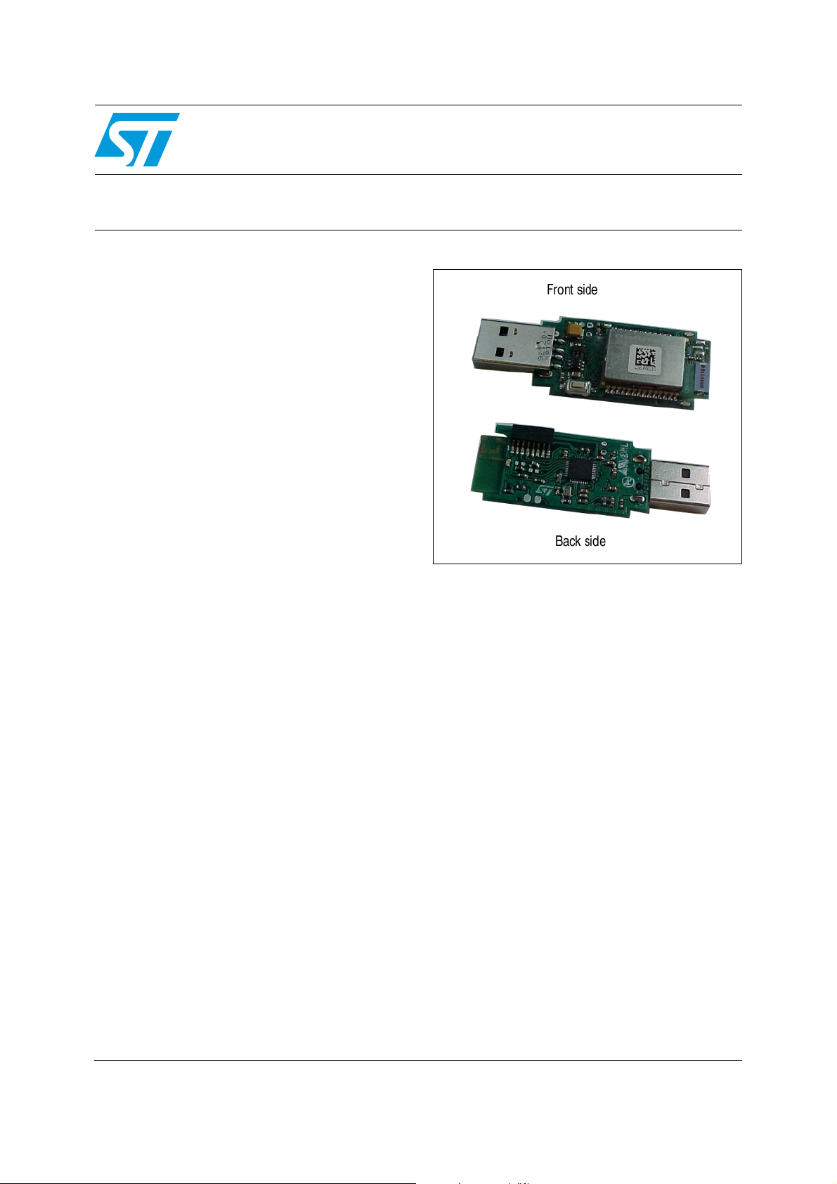
STEVAL-IDZ401V1
USB 802.15.4 dongle based on the SPZB32W1 series of modules
Data brief
Features
■ Based on a 2.4 GHz IEEE 802.15.4/ZigBee
SPZB32W1A2 RF module
■ Integrated STM32F103TBU6 with USB bridge
capabilities
■ USB interface and power supply
■ Supported reprogrammability via the USB
interface
■ JTAG connector
■ Configurable pushbutton
■ Configurable LEDs
■ Power indicator LED
■ Small dimensions 5.75 cm x 2.15 cm
■ STM32W protocol stack libraries supported
■ Supported application partitioning between
STM32F and STM32W
®
Description
The STEVAL-IDZ401V1 is an IEEE
802.15.4/ZigBee RF module with a USB interface
and with a “dongle” style optimized form factor.
The board includes an STM32F103 chipset with
USB bridge functional capabilities and an
STM32W chipset. Configurable LEDs and a
pushbutton are also available onboard.
The board supports multiple models of application
partitioning between the STM32W and the
STM32F integrated cores and is enabled to run all
the protocol stacks defined for the STM32W SoC
family.
The board allows the configuration of the
connection of the JTAG with the STM32W
(default) or with the STM32F, or with both the
processors in scan chain mode.
November 2011 Doc ID 022477 Rev 1 1/6
For further information contact your local STMicroelectronics sales office.
www.st.com
6
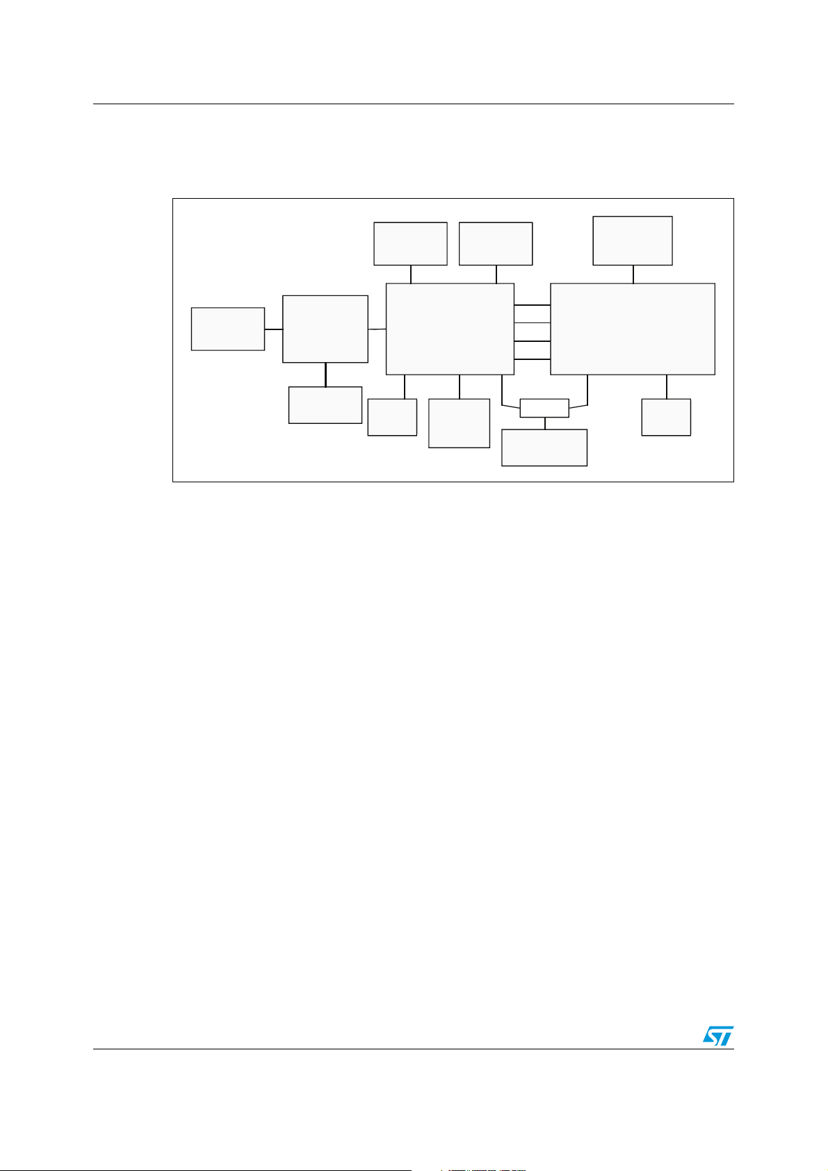
Block diagram STEVAL-IDZ401V1
1 Block diagram
Figure 1. Block diagram
USB
Connector
Supply
main
voltage
regulator
Power
LED
Prog.
Jumper
STM32F103TBU6
GPIO
Pad
Button
and LED
Prog.
16 MHz
Osc.
Prog. LED
UART
RST
Boot
GPI/O
S.C.S GPIO
JTAG
Connector
SPZB32W1x2
(802.15.4 RF Module)
Pad
2/6 Doc ID 022477 Rev 1

STEVAL-IDZ401V1 Schematic
LE
D_
32F
DI
PA7
ES E T
US
AR
T2
_TX
B
OOT
_E
N_
LOW
I/
O_
PA3
I/
O_
PA3
B
OOT
_E
N_
LOW
nR
ES E T
DO_
32W
DO
RST
MS
32F
US
AR
T2
_C
TS
US
AR
T2
_C
TS
nR
ES E T
US
AR
T2
_R
TS
32W
US
AR
T2
_RX
PB
0_
32F
CK
US
AR
T2
_R
TS
PA7
JT
DO_
32F
JT
DI_
32W
+3
.3V
+3
.3V
+3
.3V
(T
AN
T.)
USB (Vcc)
USB (D-)
USB (D+)
USB (GND)
PAD STRIP 2.54
PROGRAMMING JUMPER / PADS
(ALTERNATIVE DEVICE)
(open drain signals)
(For first programming during production)
C11
18pF
<T
yp
e>
C11
18pF
<T
yp
e>
R12
NM
R12
NM
C10
18pF<T<T
yp
e>
C10
18pF<T<T
yp
e>
U1
LDS
3985M
33R
U1
LDS
3985M
33R
Vin
1
GND
2
By
Pa
ss
4
Vo
ut
5
IN
HI
BIT
3
16
MHz
16
MHz
R5
470
Ohm
R5
470
Ohm
R2
470
Ohm
R2
470
Ohm
LE
D2
YE
LLOW
LE
D2
YE
LLOW
C12
10n<T<T
yp
e>
C12
10n<T<T
yp
e>
LE
D1
GR
EE N
LE
D1
GR
EE N
R150 0
Ohm
R150 0
Ohm
J2
1
2
3
4
5
6
7
8
TP4TPTP4
R10
100KR1R10
100K
100n
<T
yp
e>
100n
<T
yp
e>
10 KR7R7
10 K
C15
100n<T<T
yp
e>
C15
100n<T<T
yp
e>
JP1JPJP1
SW1
SW
PU
SH
BU
TT ON
SW1
SW
PU
SH
BU
TT ON
0
Ohm
0
Ohm
U1
A1
MCP
1701T-
3302E
/TT
U1
A1
MCP
1701T-
3302E
/TT
Vin
3
GND
1
Vo
ut
2
U3
US
BL
C6
-2
SC6
U3
US
BL
C6
-2
SC6
I/
O1
1
GND
2
I/
O2
3
I/
O2
4
VB
US
5
I/
O1
6
R8
1K5
R8
1K5
R4
1 K
R4
1 K
ANTENNA
ZB1
ZI
GB
E E
MO
DU
LE
S P
ZB
32W
1x2.1
ANTENNA
ZB1
ZI
GB
E E
MO
DU
LE
S P
ZB
32W
1x2.1
...
7
...
8
...
9
...
14
...
15
...
1
...
2
...
4
...
3
...
10
GND
11
V
DD (V(Vbabat)t)
12
...
21
ES E T
5
...
6
...
16
CK/
...
17
...
18
...
19
...
20
...
22
...
23
...
24
...
13
...
25
...
26
LE
D3
REDLELE
D3
RED
R1
1 0
Ohm
R1
1 0
Ohm
J1
US
B
CO
NNE
CT
OR
J1
US
B
CO
NNE
CT
OR
123
4
100n
<T
yp
e>
100n
<T
yp
e>
U2
S TM
32F
103T
BU6
U2
S TM
32F
103T
BU6
V
DD_3
1
OS
C_
IN
/P
D0
2
OS
C_
OU
T/
PD1
3
NR
ST
4
V
SS _A
5
V
DD_A
6
PA
0/
WK
UP
7
PA1
8
PA
2/
US
AR
T2
_TX
9
RX
10
SS
11
CK
12
SO
13
OSI
14
ADC
12_ININ8
15
ADC
12_ININ9
16
V
SS _1
18
V
DD_1
19
2/B
OOT1
17
PA
8/
US
AR
T1
_CK
20
PA
9/
US
AR
T1
_TX
21
PA
10/
US
AR
T1
_RX
22
PA
11/
US
BDM
23
PA
12/
US
BDP
24
PA
13/
JT
MS
/S
WD
IO
25
V
SS _2
26
V
DD_2
27
14/JTJTCKCK/S/SWCWCLKLK
28
15/JTJTDIDI
29
DO
30
ST
31
MBA
32
CL
33
DA
34
B
OOT0
35
V
SS _3
36
V
SS _EPEP
37
100n<T<T
yp
e>
100n<T<T
yp
e>
R6
470
Ohm
R6
470
Ohm
TP3TPTP3
R3
0
OHM
R3
0
OHM
10u6.6.
3V
10u6.6.
3V
C4
22u6.6.
3V
C4
22u6.6.
3V
100n
<T
yp
e>
100n
<T
yp
e>
100n
<T
yp
e>
100n
<T
yp
e>
TP2TPTP2
C3
10n
<T
yp
e>
C3
10n
<T
yp
e>
R1
3 0
Ohm
R1
3 0
Ohm
100n<T<T
yp
e>
100n<T<T
yp
e>
C14
100n
<T
yp
e>
C14
100n
<T
yp
e>
C13
100n
<T
yp
e>
C13
100n
<T
yp
e>
R9
1K5
R9
1K5
TP1TPTP1
R1
4 NM
R1
4 NM
2 Schematic
Figure 2. Schematic
US
US
USB (Vcc)
USB (D-)
USB (D+)
USB (GND)
B
B
CO
CO
NNE
NNE
J1
J1
CT
CT
OR
R1
R1
Oh
Oh
R8
R8
1K
1K
SW
SW
PU
PU
SH
SH
SW
SW
BU
BU
TTO
TTO
100n
100n
C1
C1
yp
yp
e>
e>
PB
0_
32F
R1
100K
100K
OOT
_E
nR
N_
I/
ESET
LO
O_
PA
(open drain signals)
PAD STRIP 2.54
TP
TP
J2J2J2
+3
.3
R9
R9
1K
1K
US
AR
T2
_R
18
17
16
15
14
13
12
11
10
ST
ST
32F
32F
103T
103T
BU
BU
US
AR
T2
_T
SWSWCLCLK/K/JTJTCK
JTJTDI
PCPC4/4/JTJTMS
JTJTRS
JTJTDO
nRnRESET
+3
.3
<T
<T
yp
yp
e>
e>
SS_
PBPB2/
OOT
PBPB1/1/ADC
PBPB0/0/ADC
PAPA7/7/SPSPI1I1_M_MOS
PAPA6/6/SPSPI_I_MIMISO
PAPA5/5/SPSPI1I1_S_SCK
PAPA4/4/SPSPI1I1_N_NSS
PAPA3/3/UAUARTRT2_2_RX
PBPB0_0_32W
C1
100n
C1
100n
19
20
PA
DD_1
8/
US
AR
T1
_C
12_
12_
PA
2/
US
AR
T2
_T
PA
US
US
AR
AR
T2
T2
_C
_R
TS
TS
JTJTDO
32W
R1
R1
10
10
Oh
Oh
PA
R1
R1
NM
NM
JT
R1
R1
DI
30
30
32W
Oh
Oh
R1
R1
4N
4N
JT
DO
32F
Doc ID 022477 Rev 1 3/6
OR
<T
<T
C1C1100n
C1C1100n
yp
yp
e>
C5C5100n
C5C5100n
GN
U1
MC
U1
MC
(ALTERNATIVE DEVICE)
Vi
A1
A1
1701T
1701T
Vo
ut
3302E
3302E
/T
/T
<T
<T
yp
yp
e>
e>
(T
22u
22u
3V
3V
AN
T.
e>
C2C210u
C2C210u
3V
3V
U1
U1
Vi
GN
IN
HI
BI
LD
LD
3985M
3985M
By
Pa
Vo
33R
33R
ss
ut
10n
10n
C3
C3
C4
C4
U3
US
U3
US
I/
GN
I/
O1
O2
BL
BL
C6
C6
-2
-2
VB
SC
SC
I/
I/
US
O2
O1
21
22
23
24
PA
9/
US
AR
T1
_T
PA
0/
WK
UP
25
PA
PA
PA
PA
10/
11/
12/
13/
US
US
US
JT
MS
AR
BD
BD
/S
T1
WD
_R
IO
OS
C_
OU
T/
NR
DD_A
SS_
PD
ST
C1
100n
C1
100n
<T
<T
yp
yp
e>
e>
C1
10n
C1
10n
R7R710
10
yp
yp
e>
e>
LE
RE
RE
R6
R6
D3
D3
13
PCPC1/1/...
14
PBPB0/0/...
15
PBPB1/1/...
16
PBPB2/2/...
17
JTJTCK
...
18
PCPC2/2/...
19
PCPC3/3/...
20
PCPC4/4/...
21
PCPC0/0/...
22
PBPB7/7/...
23
PBPB6/6/...
24
PAPA6/6/...
25
PAPA7/7/...
26
PCPC5/5/...
ANTENNA
ANTENNA
26
SS_
DD_2
PAPA14/
PBPB5/5/I2I2C1C1_S_SMB
PBPB6/6/I2I2C1C1_S_SCL
PBPB7/7/I2I2C1C1_S_SDA
OS
C_
IN
DD_3
/P
D0
Y1Y116
Y1Y116
LE
D_
32F
470
470
Oh
Oh
<T
<T
yp
yp
e>
e>
<T
<T
yp
yp
e>
e>
27
PAPA15/
PBPB3/3/JTJTDO
PBPB4/4/NJNJTRTRST
OOT
SS_
SS_
C1
18p
C1
18p
yp
yp
e>
e>
MH
MH
<T
<T
C1
18p
C1
18p
yp
yp
e>
e>
ZI
ZI
GB
GB
EE
EE
MO
MO
DU
DU
LE
LE
SP
SP
ZB
ZB
32W
32W
1x2.
1x2.
<T
<T
yp
yp
e>
e>
YE
YE
LLO
LLO
DD
C8C8100n
C8C8100n
C9C9100n
C9C9100n
28
29
30
31
32
33
34
35
36
37
C7C7100n
C7C7100n
LE
LE
D2
D2
GN
PAPA2/2/...
PAPA1/1/...
PAPA0/0/...
PBPB4/4/...
PBPB3/3/...
nRnRESET
PAPA3/3/...
PAPA4/4/...
PAPA5/5/...
PBPB5/5/...
yp
yp
e>
e>
LELED_D_32F
U2
U2
470
470
R5
R5
Oh
Oh
12
11
10
ZB
ZB
GR
GR
EEN
EEN
PA
PROGRAMMING JUMPER / PADS
(For first programming during production)
JP
R4
R4
1
1
Oh
Oh
+3
.3
R2
R2
470
470
LE
LE
D1
D1
Oh
Oh
C6C6100n
C6C6100n
yp
yp
e>
e>
TP
TP
0
0
OH
OH
R3
R3
US
US
AR
AR
T2
T2
_C
_R
TS
TS
R1R10
R1R10
nR
ESET
I/
O_
OOT
PA
_E
N_
LO

Main components STEVAL-IDZ401V1
3 Main components
Figure 3. Main components
JMP Boot
(STM32F)
Front
Side
Configurable
Button
(STM32F)
Configurable LEDs
(STM32F, STM32W)
SPZB32W1A2
PowerLed
Back
Side
GPIOs PADS
(STM32F, STM32W)
8 pin
JTAG Conn.
Resistorsfor JTAG
Use Conf iguration
STM32F103TB
4/6 Doc ID 022477 Rev 1

STEVAL-IDZ401V1 Revision history
4 Revision history
Table 1. Document revision history
Date Revision Changes
25-Nov-2011 1 Initial release.
Doc ID 022477 Rev 1 5/6

STEVAL-IDZ401V1
Please Read Carefully:
Information in this document is provided solely in connection with ST products. STMicroelectronics NV and its subsidiaries (“ST”) reserve the
right to make changes, corrections, modifications or improvements, to this document, and the products and services described herein at any
time, without notice.
All ST products are sold pursuant to ST’s terms and conditions of sale.
Purchasers are solely responsible for the choice, selection and use of the ST products and services described herein, and ST assumes no
liability whatsoever relating to the choice, selection or use of the ST products and services described herein.
No license, express or implied, by estoppel or otherwise, to any intellectual property rights is granted under this document. If any part of this
document refers to any third party products or services it shall not be deemed a license grant by ST for the use of such third party products
or services, or any intellectual property contained therein or considered as a warranty covering the use in any manner whatsoever of such
third party products or services or any intellectual property contained therein.
UNLESS OTHERWISE SET FORTH IN ST’S TERMS AND CONDITIONS OF SALE ST DISCLAIMS ANY EXPRESS OR IMPLIED
WARRANTY WITH RESPECT TO THE USE AND/OR SALE OF ST PRODUCTS INCLUDING WITHOUT LIMITATION IMPLIED
WARRANTIES OF MERCHANTABILITY, FITNESS FOR A PARTICULAR PURPOSE (AND THEIR EQUIVALENTS UNDER THE LAWS
OF ANY JURISDICTION), OR INFRINGEMENT OF ANY PATENT, COPYRIGHT OR OTHER INTELLECTUAL PROPERTY RIGHT.
UNLESS EXPRESSLY APPROVED IN WRITING BY TWO AUTHORIZED ST REPRESENTATIVES, ST PRODUCTS ARE NOT
RECOMMENDED, AUTHORIZED OR WARRANTED FOR USE IN MILITARY, AIR CRAFT, SPACE, LIFE SAVING, OR LIFE SUSTAINING
APPLICATIONS, NOR IN PRODUCTS OR SYSTEMS WHERE FAILURE OR MALFUNCTION MAY RESULT IN PERSONAL INJURY,
DEATH, OR SEVERE PROPERTY OR ENVIRONMENTAL DAMAGE. ST PRODUCTS WHICH ARE NOT SPECIFIED AS "AUTOMOTIVE
GRADE" MAY ONLY BE USED IN AUTOMOTIVE APPLICATIONS AT USER’S OWN RISK.
Resale of ST products with provisions different from the statements and/or technical features set forth in this document shall immediately void
any warranty granted by ST for the ST product or service described herein and shall not create or extend in any manner whatsoever, any
liability of ST.
ST and the ST logo are trademarks or registered trademarks of ST in various countries.
Information in this document supersedes and replaces all information previously supplied.
The ST logo is a registered trademark of STMicroelectronics. All other names are the property of their respective owners.
© 2011 STMicroelectronics - All rights reserved
STMicroelectronics group of companies
Australia - Belgium - Brazil - Canada - China - Czech Republic - Finland - France - Germany - Hong Kong - India - Israel - Italy - Japan -
Malaysia - Malta - Morocco - Philippines - Singapore - Spain - Sweden - Switzerland - United Kingdom - United States of America
www.st.com
6/6 Doc ID 022477 Rev 1
 Loading...