

Offline LED driver with primary-sensing and
Features
■ High power factor capability (> 0.9)
■ 800 V, avalanche rugged internal 11 Ω power
MOSFET
■ Internal high-voltage startup
■ Primary sensing regulation (PSR)
■ +/- 5% accuracy on constant LED output
current
■ Quasi-resonant (QR) operation
■ Optocoupler not needed
■ Open or short LED string management
■ Automatic self supply
Applications
HVLED807PF
high power factor up to 7 W
Datasheet − preliminary data
SO16N
Table 1. Device summary
Order code Package Packaging
■ AC-DC LED driver bulb replacement lamps up
to 7 W, with high power factor
■ AC-DC LED drivers up to 7 W
Description
The HVLED807PF is a high-voltage primary
switcher intended to operate directly from the
rectified mains with minimum external parts and
enabling high power factor (> 0.90) to provide an
efficient, compact and cost effective solution for
LED driving. It combines a high-performance lowvoltage PWM controller chip and an 800 V,
avalanche-rugged Power MOSFET, in the same
package. There is no need for an optocoupler
thanks to the patented primary sensing regulation
(PSR) technique. The device assures protection
against LED string fault (open or short).
HVLED807PF
SO16N
Tu be
HVLED807PFTR Tape & Reel
July 2012 Doc ID 023464 Rev 1 1/17
This is preliminar y information on a new product now in development or undergoing evaluation. Details are subject to
change without notice.
www.st.com
17

Contents HVLED807PF
Contents
1 Principle application circuit and block diagram . . . . . . . . . . . . . . . . . . . 3
1.1 Principle application circuit . . . . . . . . . . . . . . . . . . . . . . . . . . . . . . . . . . . . . 3
1.2 Block diagram . . . . . . . . . . . . . . . . . . . . . . . . . . . . . . . . . . . . . . . . . . . . . . . 5
2 Pin description and connection diagrams . . . . . . . . . . . . . . . . . . . . . . . 6
2.1 Thermal data . . . . . . . . . . . . . . . . . . . . . . . . . . . . . . . . . . . . . . . . . . . . . . . 6
3 Electrical specifications . . . . . . . . . . . . . . . . . . . . . . . . . . . . . . . . . . . . . . 7
3.1 Absolute maximum ratings . . . . . . . . . . . . . . . . . . . . . . . . . . . . . . . . . . . . . 7
3.2 Electrical characteristics . . . . . . . . . . . . . . . . . . . . . . . . . . . . . . . . . . . . . . . 7
4 Device description . . . . . . . . . . . . . . . . . . . . . . . . . . . . . . . . . . . . . . . . . 13
5 Package information . . . . . . . . . . . . . . . . . . . . . . . . . . . . . . . . . . . . . . . . 14
6 Revision history . . . . . . . . . . . . . . . . . . . . . . . . . . . . . . . . . . . . . . . . . . . 17
2/17 Doc ID 023464 Rev 1
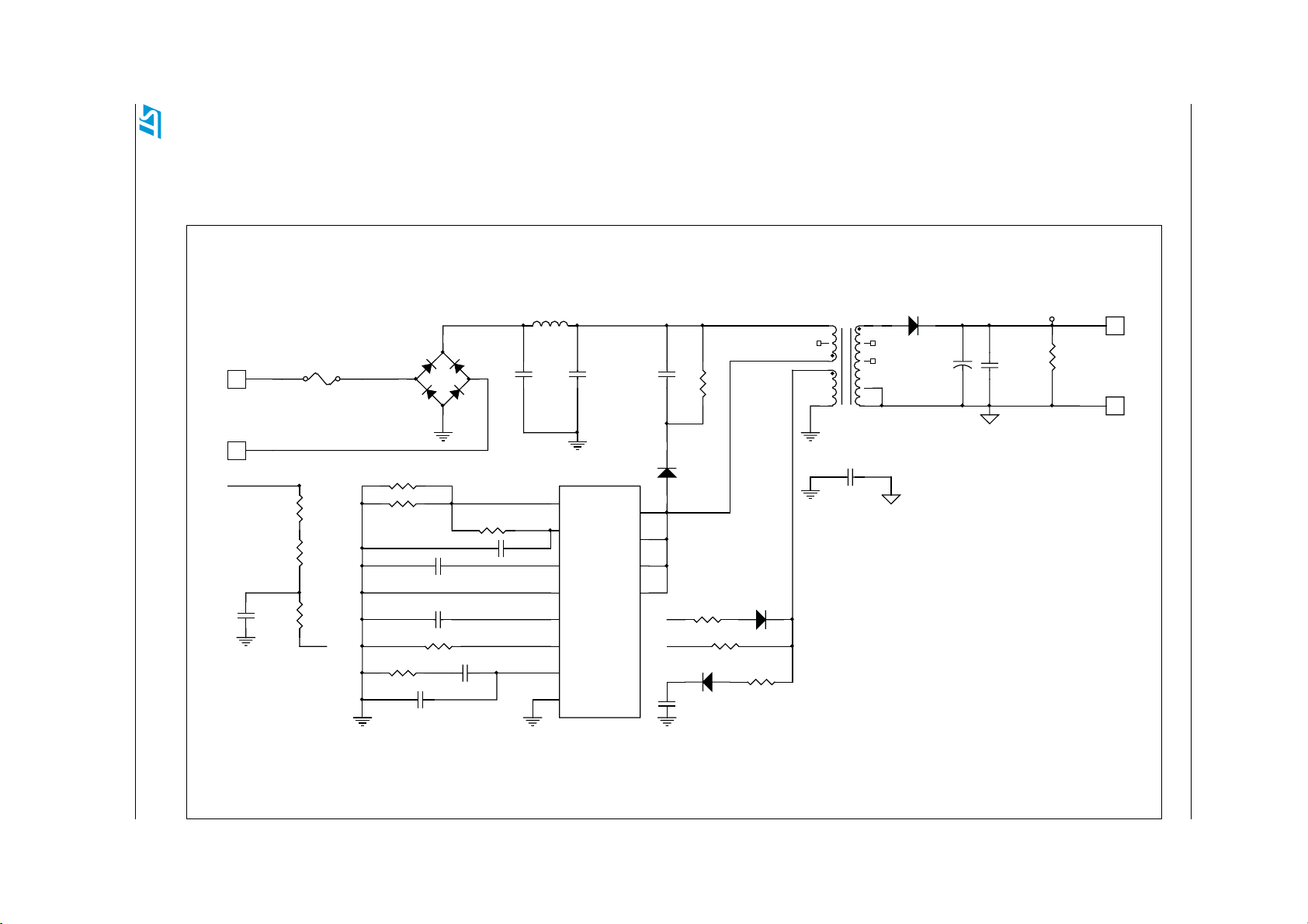
1 Principle application circuit and block diagram
1.1 Principle application circuit
Figure 1. Principle application circuit for high power factor LED driver
HVLED807PF Principle application circuit and block diagram
Doc ID 023464 Rev 1 3/17
J2
CON1
J4
CON1
VIN
COS Filter (1uF)
34
Bridge Diode
F1 1A_DIP
RA
RB
ROS
CS DMG
2 1
C_Vcc (10uF)
C_ILED (10uF)
Rf (8.2k-15k)
+
-
Rsens e
Rsens e
R1 (1k8-2k2)
220pF-330pF
Rfb
Cf (330nF/ 680nF)
Cp (1nF/ 10nF)
Lin (330uH - 820uH)
Cin - (22nF / 47nF)
U1
HVLED8xxPF
1
SOURCE
2
CS
CS
3
VCC
VCC
4
GND
5
ILED
6
DMG
7
COMP
8
NA
N.A.
Cin - (22nF / 47nF)
DRAIN
DRAIN
DRAIN
DRAIN
Csnubber (1nF )
16
15
14
13
VIN
Rsnubber (120k )
S n ubber Diode
CS
RPF
DMG
VCC
C_VCC (470nF)
Rdmg
D2
1N4148
D4
R-VCC (10ohm)
T1
1 10
2
3
4
5 6
TRA NSFORMER
C10
Y1 - SAFETY
O utpo ut Diode
9
8
7
C12
Cout Bulk
C13
Cout SMD
Vout
R12
Mini mum Load
J1
CON1
J3
CON1
AM13207v1
4/17 Doc ID 023464 Rev 1
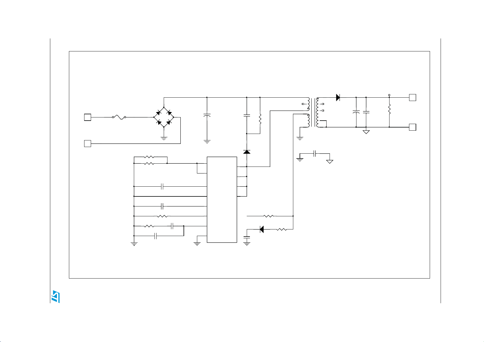
Figure 2. Principle application circuit for standard LED driver
Principle application circuit and block diagram HVLED807PF
J7
CON1
J8
CON1
F2 1A_DIP
Bridge Diode
2 1
Rsens e
Rsens e
C_Vcc (10uF)
C_ILED (10uF)
Rfb
Rf (8.2k -15k)
Cp (1nF/ 10nF)
34
+
-
Cf (330nF/ 680nF)
VCC
DMG
1
2
3
4
5
6
7
8
NA
C22
Cin
U2
HVLED8xxPF
SOURC E
CS
VCC
GND
ILED
DMG
COMP
N.A.
DRAIN
DRAIN
DRAIN
DRAIN
Csnubber (1nF )
16
15
14
13
VIN
Rsnubber (120k )
S n ubber Diode
DMG
VCC
C_VCC (470nF)
Rdmg
D6
1N4148
R-VCC (10ohm)
T2
1 10
2
3
4
5 6
TRA NSFORMER
C21
Y1 - SAFETY
O utpo ut Diode1
9
8
7
C15
Cout Bulk
C23
Cout SMD
Vout
R16
Minimum Load
J5
CON1
J6
CON1
AM13208v1
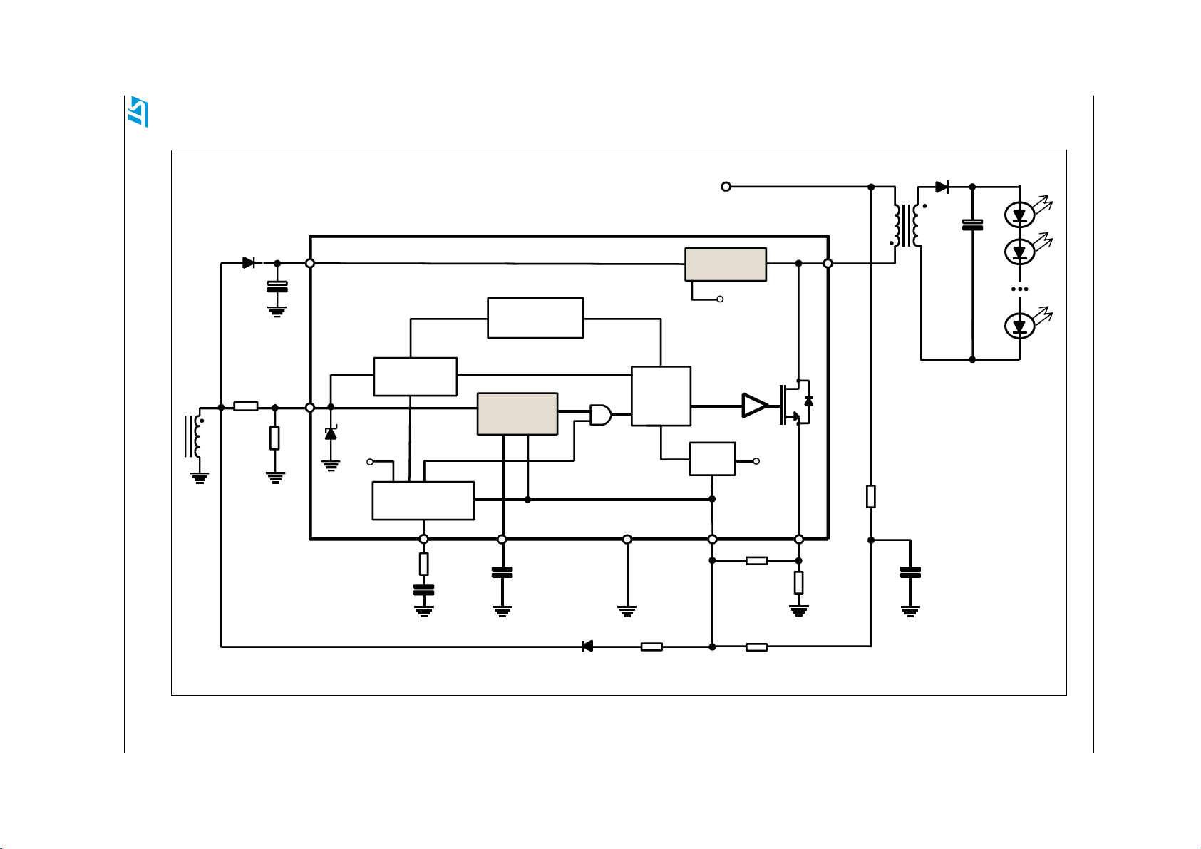
1.2 Block diagram
Figure 3. Block diagram
HVLED807PF Principle application circuit and block diagram
+ VIN
Doc ID 023464 Rev 1 5/17
VCC
PROTECTION &
FEEDFORWARD
LOGIC
DEMAG
R
DMG
DMG
R
FB
3.3 V
LOGIC
Vref
Constant Voltage
Regulation
COMP
R
COMP
C
COMP
CONSTANT
CURRENT
REGULATION
VILED
ILED
C
VCS
LED
GND
DRIVING
LOGIC
R
PF
HV start-up &
Supply Logic
Vref
OCP
CS
DRAIN
1 V
R
A
R
1
R
OS
SOURCE
R
SENSE
LED
AM13209v1
Pin description and connection diagrams HVLED807PF
A
A
A
2 Pin description and connection diagrams
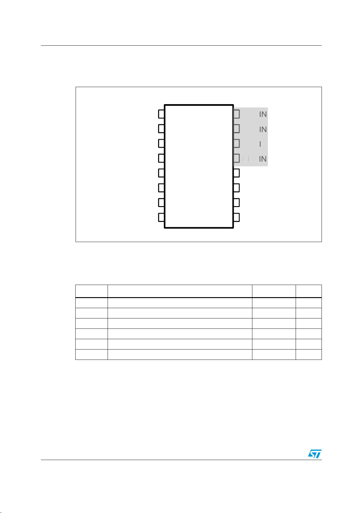
Figure 4. Pin connection (top view)
SOURCE
2.1 Thermal data
Table 2. Thermal data
Symbol Parameter Max. value Unit
CS
VCC
GND
ILED
DMG
COMP
N.A.
1
1
2
2
3
3
4
4
5
5
6
6
7
7
8
8
16
16
15
15
14
14
13
13
12
12
11
11
10
10
DRAIN
DRAIN
DRAIN
N
DRAIN
N.C.
N.A.
N.A.
9
9
N.A.
AM13210v1
R
thJP
R
thJA
P
TOT
T
MAX
T
STG
T
6/17 Doc ID 023464 Rev 1
Thermal resistance, junction-to-pin 10 °C/W
Thermal resistance, junction-to-ambient 110 °C/W
Maximum power dissipation at TA = 50 °C 0.9 W
Maximum junction temperature 150 °C
Storage temperature range -55 to 150 °C
Junction temperature range -40 to 125 °C
J

HVLED807PF Electrical specifications
3 Electrical specifications
3.1 Absolute maximum ratings
Table 3. Absolute maximum ratings
Symbol Pin Parameter Value Unit
V
DS
I
D
Eav 1, 13-16
1, 13-16 Drain-to-source (ground) voltage -1 to 800 V
1, 13-16 Drain current
Single-pulse avalanche energy
(Tj = 25 °C, I
Vcc 3 Supply voltage (Icc < 25 mA) Self limiting V
I
DMG
V
CS
6 Zero current detector current ±2 mA
2 Current sense analog input -0.3 to 3.6 V
Vcomp 7 Analog input -0.3 to 3.6 V
1. Limited by maximum temperature allowed.
3.2 Electrical characteristics
Table 4. Electrical characteristics
Symbol Parameter Test condition Min. Typ. Max. Unit
Power section
V
(BR)DSS
I
DSS
Drain-source breakdown ID < 100 µA; Tj = 25 °C 800 V
OFF-state drain current
(1)
= 0.7 A)
D
(1) (2)
= 750 V; Tj = 125 °C
V
DS
(3)
, see
Figure 5
1A
50 mJ
80 µA
R
DS(on)
C
OSS
Drain-source ON-state
resistance
Effective (energy-related)
output capacitance
High-voltage startup generator
V
START
I
CHARGE
V
CC_RESTART
Min. drain start voltage I
Vcc startup charge current
Vcc restart voltage
(Vcc falling)
Id=250 mA; Tj = 25 °C 6 7.4
Id=250 mA; Tj = 125 °C
(3)
(3)
See
Figure 6
< 100 µA 40 50 60 V
charge
> V
V
DRAIN
Vcc < Vcc
Start
On
;
45.57
Tj = 25 °C
> V
V
DRAIN
Vcc < Vcc
(4)
Start
On
;
+/- 10%
9.5 10.5 11.5 V
14.8
Ω
mA
After protection tripping 5
Doc ID 023464 Rev 1 7/17

Electrical specifications HVLED807PF
Table 4. Electrical characteristics
(1) (2)
(continued)
Symbol Parameter Test condition Min. Typ. Max. Unit
Supply voltage
Vcc Operating range After turn-on 11.5 23
V
CC_ON
V
CC_OFF
V
Turn-on threshold
Turn-off threshold
Z
Internal Zener voltage Icc = 20 mA 23 25 27 V
(4)
(4)
12 13 14 V
91011V
Supply current
I
CC_START-UP
Iq Quiescent current See
I
CC
Iq
(fault)
Startup current See
Operating supply current
at 50 kHz
See
Fault quiescent current See
Figure 7
Figure 8
Figure 9
Figure 10
200 300 µA
11.4mA
1.4 1.7 mA
250 350 µA
Startup timer
T
START
T
RESTART
Start timer period 105 140 175 µs
Restart timer period
during burst mode
420 500 700 µs
Demagnetization detector
I
Dmgb
V
DMGH
V
DMGL
V
DMGA
V
DMGT
T
BLANK
Input bias current V
Upper clamp voltage I
Lower clamp voltage I
Arming voltage Positive-going edge 100 110 120 mV
Triggering voltage Negative-going edge 50 60 70 mV
Trigger blanking time after
MOSFET turn-off
= 0.1 to 3 V 0.1 1 µA
DMG
= 1 mA 3.0 3.3 3.6 V
DMG
= - 1 mA -90 -60 -30 mV
DMG
V
≥ 1.3 V 6
COMP
= 0.9 V 30
V
COMP
Line feedforward
µs
R
FF
Equivalent feedforward
resistor
I
= 1 mA 45 Ω
DMG
Transconductance error amplifier
T
j = 25 °C 2.45 2.51 2.57
V
REF
Voltage reference
(3)
Tj = -25 to 125 °C and
Vcc = 12 V to 23 V
= ± 10 µA
∆I
gm Transconductance
Gv Voltage gain
GB Gain-bandwidth product
COMP
V
= 1.65 V
COMP
(5)
Open loop 73 dB
(5)
8/17 Doc ID 023464 Rev 1
2.4 2.6
V
1.3 2.2 3.2 ms
500 KHz

HVLED807PF Electrical specifications
Table 4. Electrical characteristics
(1) (2)
(continued)
Symbol Parameter Test condition Min. Typ. Max. Unit
= 2.3 V,
V
DMG
= 1.65 V
V
COMP
= 2.7 V,
V
DMG
= 1.65 V
V
COMP
= 2.3 V 2.7 V
DMG
= 2.7 V 0.7 V
DMG
70 100 µA
400 750 µA
I
COMP
V
COMPH
V
COMPL
V
COMPBM
Source current
Sink current
Upper COMP voltage V
Lower COMP voltage V
Burst-mode threshold 1 V
Hys Burst-mode hysteresis 65 mV
Current reference
V
V
ILEDx
CLED
Maximum value V
COMP
= V
COMPL
1.5 1.6 1.7 V
Current reference voltage 0.192 0.2 0.208 V
Current sense
t
LEB
T
D
V
CSx
V
CSdis
1. Vcc=14 V (unless otherwise specified).
2. Limits are production tested at Tj=Ta=25 °C, and are guaranteed by statistical characterization in the range
Tj 25-125
3. Not production tested, guaranteed statistical characterization only.
4. Parameters tracking each other (in the same section).
5. Guaranteed by design.
Leading-edge blanking
Delay-to-output (H-L) 90 200 ns
Max. clamp value
Hiccup-mode OCP level
°C.
(5)
(4)
dVcs/dt = 200 mV/µs 0.7 0.75 0.8 V
(4)
0.92 1 1.08 V
330 ns
Figure 5. OFF-state drain and source current test circuit
DM G
2.5V
14V
VDD
+
-
COMP SOURCE
ILED
CU RRE NT
CONTROL
GND
CS
DR AIN
Idss
A
AM13211v1
Note: The measured IDSS is the sum between the current across the startup resistor and the
effective
MOSFET’s
OFF-state drain current.
Doc ID 023464 Rev 1 9/17
Vin
750V

Electrical specifications HVLED807PF
Figure 6. COSS output capacitance variation
600
500
400
300
Coss [pF]
200
100
0
0 25 50 75 100 125 150
Vds [ V]
AM13212v1
Figure 7. Startup current test circuit
DMG
2.5V
11.8 V
+
Iccstart-up
A
VDD
CURRENT
CONTROL
-
COM P SOURCE
ILED
GND
CS
DRAIN
AM13213v1
10/17 Doc ID 023464 Rev 1

HVLED807PF Electrical specifications
Figure 8. Quiescent current test circuit
Iq_meas
VDD
2.5V
+
DMG
33k
3V
-
COM P SOURCE
ILED
0.8V
Figure 9. Operating supply current test circuit
Icc
27k
220k
10k
10k
DMG
2.5V
+
-
COM P SOURCE
A
VDD
CURR ENT
CONTROL
GND
ILED
CS
CURR ENT
CON TROL
GND
14VA
DRAIN
10k
15V
DRAIN
CS
0.2V
AM13214v1
1.5K 2W
150V
50 kHz
10
-5V
2.8V
Note: The circuit across the DMG pin is used for switch-on synchronization.
Figure 10. Quiescent current during fault test circuit
DMG
2.5V
Iq(fault)
A
VDD
+
-
COM P SOURCE
ILED
CURRENT
CON TROL
GND
14V
CS
5.6
AM13215v1
DRAIN
AM13216v1
Doc ID 023464 Rev 1 11/17

Device description HVLED807PF
4 Device description
The HVLED807PF is a high-voltage primary switcher intended to operate directly from the
rectified mains with minimum external parts to provide high power factor (> 0.90) and an
efficient, compact and cost effective solution for LED driving. It combines a highperformance low-voltage PWM controller chip and an 800 V, avalanche-rugged Power
MOSFET, in the same package.
The PWM is a current-mode controller IC specifically designed for ZVS (zero voltage
switching) flyback LED drivers, with constant output current (CC) regulation using primary
sensing feedback (PSR). This eliminates the need for the optocoupler, the secondary
voltage reference, as well as the current sense on the secondary side, while still maintaining
a good LED current accuracy. Moreover, it guarantees a safe operation when short-circuit of
one or more LEDs occurs.
The device can also provide a constant output voltage regulation (CV): it allows the
application to be able to work safely when the LED string opens due to a failure.
In addition, the device offers the shorted secondary rectifier (i.e. LED string shorted due to a
failure) or transformer saturation detection.
Quasi-resonant operation is achieved by means of a transformer demagnetization sensing
input that triggers MOSFET turn-on. This input serves also as both output voltage monitor,
to perform CV regulation, and input voltage monitor, to achieve mains-independent CC
regulation (line voltage feedforward).
The maximum switching frequency is top-limited below 166 kHz, so that at medium-light
load a special function automatically lowers the operating frequency still maintaining the
operation as close to ZVS as possible. At very light load, the device enters a controlled
burst-mode operation that, along with the built-in high-voltage startup circuit and the low
operating current of the device, helps minimize the residual input consumption.
Although an auxiliary winding is required in the transformer to correctly perform CV/CC
regulation, the chip is able to power itself directly from the rectified mains. This is useful
especially during CC regulation, where the flyback voltage generated by the winding drops.
12/17 Doc ID 023464 Rev 1

HVLED807PF Package information
5 Package information
In order to meet environmental requirements, ST offers these devices in different grades of
®
ECOPACK
specifications, grade definitions and product status are available at:
packages, depending on their level of environmental compliance. ECOPACK
www.st.com
.
ECOPACK is an ST trademark.
Figure 11. SO16N mechanical data
mm
Dim.
Min. Typ. Max.
A 1.75
A1 0.10 0.25
A2 1.25
b0.31 0.51
c0.17 0.25
D 9.80 9.90 10.00
E5.806.006.20
E1 3.80 3.90 4.00
e1.27
h0.25 0.50
L0.40 1.27
k0 8°
ccc 0.10
Doc ID 023464 Rev 1 13/17

Package information HVLED807PF
Figure 12. SO16N drawing
14/17 Doc ID 023464 Rev 1
0016020_F

HVLED807PF Package information
Figure 13. SO16N recommended footprint (dimensions are in mm)
Doc ID 023464 Rev 1 15/17

Revision history HVLED807PF
6 Revision history
Table 5. Document revision history
Date Revision Changes
26-Jul-2012 1 Initial release.
16/17 Doc ID 023464 Rev 1

HVLED807PF
Please Read Carefully:
Information in this document is provided solely in connection with ST products. STMicroelectronics NV and its subsidiaries (“ST”) reserve the
right to make changes, corrections, modifications or improvements, to this document, and the products and services described herein at any
time, without notice.
All ST products are sold pursuant to ST’s terms and conditions of sale.
Purchasers are solely responsible for the choice, selection and use of the ST products and services described herein, and ST assumes no
liability whatsoever relating to the choice, selection or use of the ST products and services described herein.
No license, express or implied, by estoppel or otherwise, to any intellectual property rights is granted under this document. If any part of this
document refers to any third party products or services it shall not be deemed a license grant by ST for the use of such third party products
or services, or any intellectual property contained therein or considered as a warranty covering the use in any manner whatsoever of such
third party products or services or any intellectual property contained therein.
UNLESS OTHERWISE SET FORTH IN ST’S TERMS AND CONDITIONS OF SALE ST DISCLAIMS ANY EXPRESS OR IMPLIED
WARRANTY WITH RESPECT TO THE USE AND/OR SALE OF ST PRODUCTS INCLUDING WITHOUT LIMITATION IMPLIED
WARRANTIES OF MERCHANTABILITY, FITNESS FOR A PARTICULAR PURPOSE (AND THEIR EQUIVALENTS UNDER THE LAWS
OF ANY JURISDICTION), OR INFRINGEMENT OF ANY PATENT, COPYRIGHT OR OTHER INTELLECTUAL PROPERTY RIGHT.
UNLESS EXPRESSLY APPROVED IN WRITING BY TWO AUTHORIZED ST REPRESENTATIVES, ST PRODUCTS ARE NOT
RECOMMENDED, AUTHORIZED OR WARRANTED FOR USE IN MILITARY, AIR CRAFT, SPACE, LIFE SAVING, OR LIFE SUSTAINING
APPLICATIONS, NOR IN PRODUCTS OR SYSTEMS WHERE FAILURE OR MALFUNCTION MAY RESULT IN PERSONAL INJURY,
DEATH, OR SEVERE PROPERTY OR ENVIRONMENTAL DAMAGE. ST PRODUCTS WHICH ARE NOT SPECIFIED AS "AUTOMOTIVE
GRADE" MAY ONLY BE USED IN AUTOMOTIVE APPLICATIONS AT USER’S OWN RISK.
Resale of ST products with provisions different from the statements and/or technical features set forth in this document shall immediately void
any warranty granted by ST for the ST product or service described herein and shall not create or extend in any manner whatsoever, any
liability of ST.
ST and the ST logo are trademarks or registered trademarks of ST in various countries.
Information in this document supersedes and replaces all information previously supplied.
The ST logo is a registered trademark of STMicroelectronics. All other names are the property of their respective owners.
© 2012 STMicroelectronics - All rights reserved
STMicroelectronics group of companies
Australia - Belgium - Brazil - Canada - China - Czech Republic - Finland - France - Germany - Hong Kong - India - Israel - Italy - Japan -
Malaysia - Malta - Morocco - Philippines - Singapore - Spain - Sweden - Switzerland - United Kingdom - United States of America
www.st.com
Doc ID 023464 Rev 1 17/17
 Loading...