

Off-line LED driver with primary-sensing
Features
■ 800 V, avalanche rugged internal power
MOSFET
■ 5% accuracy on constant LED output current
with primary control
■ Optocoupler not needed
■ Quasi-resonant (QR) zero voltage switching
(ZVS) operation
■ Internal HV start-up circuit
■ Open or short LED string management
■ Automatic self supply
■ Input voltage feed-forward for mains
independent cc regulation
HVLED805
SO16N
Table 1. Device summary
Order codes Package Packaging
HVLED805
SO16N
HVLED805TR Tape and reel
Tube
Applications
■ AC-DC led driver applications
■ LED retrofit lamps (i.e. E27, GU10)
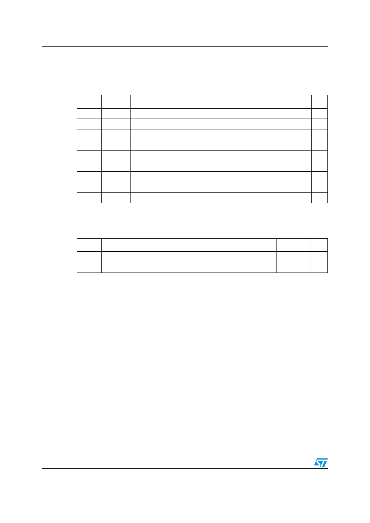
Figure 1. Application diagram
VCC
PROTECTION &
FEEDFORWARD
LOGIC
DE MAG
Rdmg
DMG
Rfb
3.3V
LOG IC
Vref
CONSTANT
VOLT AGE
REGULATION
CONSTANT
CURRENT
REGULATION
Vc
COMP ILED GND SOURCE
Rcomp
Ccomp
CLED
DRIVING
LOGIC
HV start-u p &
SUPPLY LOGIC
Vref
1V
OCP
Vin
DRAIN
LED
...
Rsens e
October 2010 Doc ID 18077 Rev 1 1/29
www.st.com
29

Contents HVLED805
Contents
1 Description . . . . . . . . . . . . . . . . . . . . . . . . . . . . . . . . . . . . . . . . . . . . . . . . . 3
2 Maximum ratings . . . . . . . . . . . . . . . . . . . . . . . . . . . . . . . . . . . . . . . . . . . . 4
3 Electrical characteristics . . . . . . . . . . . . . . . . . . . . . . . . . . . . . . . . . . . . . 5
4 Pin connection . . . . . . . . . . . . . . . . . . . . . . . . . . . . . . . . . . . . . . . . . . . . . . 7
5 Application information . . . . . . . . . . . . . . . . . . . . . . . . . . . . . . . . . . . . . 12
5.1 Power section and gate driver . . . . . . . . . . . . . . . . . . . . . . . . . . . . . . . . . 13
5.2 High voltage startup generator . . . . . . . . . . . . . . . . . . . . . . . . . . . . . . . . . 13
5.3 Secondary side demagnetization detection and triggering block . . . . . . . 15
5.4 Constant voltage operation . . . . . . . . . . . . . . . . . . . . . . . . . . . . . . . . . . . 16
5.5 Constant current operation . . . . . . . . . . . . . . . . . . . . . . . . . . . . . . . . . . . . 18
5.6 Voltage feedforward block . . . . . . . . . . . . . . . . . . . . . . . . . . . . . . . . . . . . 20
5.7 Burst-mode operation at no load or very light load . . . . . . . . . . . . . . . . . . 22
5.8 Soft-start and starter block . . . . . . . . . . . . . . . . . . . . . . . . . . . . . . . . . . . . 23
5.9 Hiccup mode OCP . . . . . . . . . . . . . . . . . . . . . . . . . . . . . . . . . . . . . . . . . . 23
5.10 Layout recommendations . . . . . . . . . . . . . . . . . . . . . . . . . . . . . . . . . . . . . 24
6 Package mechanical data . . . . . . . . . . . . . . . . . . . . . . . . . . . . . . . . . . . . 26
7 Revision history . . . . . . . . . . . . . . . . . . . . . . . . . . . . . . . . . . . . . . . . . . . 28
2/29 Doc ID 18077 Rev 1

HVLED805 Description
1 Description
The HVLED805 is a high-voltage primary switcher intended for operating directly from the
rectified mains with minimum external parts to provide an efficient, compact and cost
effective solution for LED driving. It combines a high-performance low-voltage PWM
controller chip and an 800V, avalanche-rugged power MOSFET, in the same package.
The PWM is a current-mode controller IC specifically designed for ZVS (zero voltage
switching) fly-back LED drivers, with constant output current (CC) regulation using primarysensing feedback. This eliminates the need for the opto-coupler, the secondary voltage
reference, as well as the current sense on the secondary side, still maintaining a good LED
current accuracy. Moreover it guarantees a safe operation when short circuit of one or more
LEDs occurs.
In addition, the device can also provide a constant output voltage regulation (CV): it makes
the application able to work safely when the LED string opens due to a failure.
Quasi-resonant operation is achieved by means of a transformer demagnetization sensing
input that triggers MOSFET’s turn-on. This input serves also as both output voltage monitor,
to perform CV regulation, and input voltage monitor, to achieve mains-independent CC
regulation (line voltage feed forward).
The maximum switching frequency is top-limited below 166 kHz, so that at medium-light
load a special function automatically lowers the operating frequency still maintaining the
operation as close to ZVS as possible. At very light load, the device enters a controlled
burst-mode operation that, along with the built-in high-voltage start-up circuit and the low
operating current of the device, helps minimize the residual input consumption.
Although an auxiliary winding is required in the transformer to correctly perform CV/CC
regulation, the chip is able to power itself directly from the rectified mains. This is useful
especially during CC regulation, where the fly-back voltage generated by the winding drops.
In addition to these functions that optimize power handling under different operating
conditions, the device offers protection features that considerably increase end-product’s
safety and reliability: auxiliary winding disconnection or brownout detection and shorted
secondary rectifier or transformer’s saturation detection. All of them are auto restart mode.
Doc ID 18077 Rev 1 3/29
Maximum ratings HVLED805
2 Maximum ratings
Table 2. Absolute maximum ratings
Symbol Pin Parameter Value Unit
V
I
V
T
1. Limited by maximum temperature allowed.
1,2, 13-16 Drain-to-source (ground) voltage -1 to 800 V
DS
1,2, 13-16 Drain current
I
D
1,2, 13-16 Single pulse avalanche energy (Tj = 25°C, ID = 0.7A) 50 mJ
E
av
V
cc
DMG
comp
P
tot
T
J
stg
3 Supply voltage (Icc < 25mA) Self limiting V
6 Zero current detector current ±2 mA
7 Analog input -0.3 to 3.6 V
Power dissipation @TA = 50°C 0.9 W
Junction temperature range -40 to 150 °C
Storage temperature -55 to 150 °C
(1)
1A
Table 3. Thermal data
Symbol Parameter Max. value Unit
R
R
Thermal resistance, junction-to-pin 10
thJP
Thermal resistance, junction-to-ambient 110
thJA
°C/W
4/29 Doc ID 18077 Rev 1
HVLED805 Electrical characteristics
3 Electrical characteristics
TJ = -25 to 125 °C, Vcc=14 V; unless otherwise specified.
Table 4. Electrical characteristics
Symbol Parameter Test condition Min. Typ. Max. Unit
Power section
V
(BR)DSS
I
DSS
Drain-source breakdown ID< 100 µA; Tj = 25 °C 800 V
V
= 750V; Tj = 125 °C
Off state drain current
DS
(See Figure 4 and note)
80 µA
Id=250 mA; Tj = 25 °C 11 14
R
DS(on)
C
Drain-source ON-state resistance
Effective (energy-related) output capacitance (See Figure 3)
oss
Id=250 mA; Tj = 125 °C 28
High-voltage start-up generator
V
Start
I
charge
V
CCrestart
Min. drain start voltage I
Vcc startup charge current
Vcc restart voltage
(Vcc falling)
< 100µA 40 50 60 V
charge
> V
> V
; Vcc<Vcc
Start
; Vcc<Vcc
Start
On,
On
45.57
+/-10%
9.5 10.5 11.5
V
DRAIN
Tj = 25 °C
V
DRAIN
(1)
After protection tripping 5
Supply voltage
Vcc Operating range After turn-on 11.5 23 V
Vcc
Vcc
Turn-on threshold
On
Turn-off threshold
Off
V
Zener voltage Icc = 20mA 23 25 27 V
Z
(1)
(1)
12 13 14 V
91011V
Supply current
Ω
mA
V
Icc
start-up
Start-up current (See Figure 5) 200 300 µA
Iq Quiescent current (See Figure 6)11.4mA
Icc Operating supply current @ 50 kHz (See Figure 7)1.41.7mA
Iq
(fault)
Fault quiescent current
During hiccup and brownout
(See Figure 8)
250 350 µA
Start-up timer
T
RESTART
T
START
Start timer period 105 140 175 µs
Restart timer period during burst mode 420 500 700 µs
Demagnetization detector
I
DMGb
Input bias current V
= 0.1 to 3V 0.1 1 µA
DMG
Doc ID 18077 Rev 1 5/29
Electrical characteristics HVLED805
Table 4. Electrical characteristics (continued)
Symbol Parameter Test condition Min. Typ. Max. Unit
V
DMGH
V
DMGL
V
DMGA
V
DMGT
I
DMGON
T
BLANK
Upper clamp voltage I
Lower clamp voltage I
= 1 mA 3.0 3.3 3.6 V
DMG
= - 1 mA -90 -60 -30 mV
DMG
Arming voltage positive-going edge 100 110 120 mV
Triggering voltage negative-going edge 50 60 70 mV
Min. source current during MOSFET ON-time -25 -50 -75 µA
V
≥ 1.3V 6
Trigger blanking time after MOSFET’s turn-off
COMP
= 0.9V 30
V
COMP
Line feedforward
R
Equivalent feedforward resistor I
FF
= 1mA 45 Ω
DMG
Transconductance error amplifier
(1)
= ±10 µA
= 1.65 V
(1)
2.45 2.51 2.57
2.4 2.6
1.3 2.2 3.2 mS
V
REF
Voltage reference
gm Transconductance
Tj = 25 °C
Tj = -25 to 125°C and
Vcc=12V to 23V
ΔI
COMP
V
COMP
Gv Voltage gain Open loop 73 dB
GB Gain-bandwidth product 500 kHz
I
COMP
V
COMPH
V
COMPL
V
COMPBM
Source current V
Sink current V
Upper COMP voltage V
Lower COMP voltage V
Burst-mode threshold 1 V
= 2.3V, V
DMG
= 2.7V, V
DMG
= 2.3V 2.7 V
DMG
= 2.7V 0.7 V
DMG
= 1.65V 70 100 µA
COMP
= 1.65V 400 750 µA
COMP
Hys Burst-mode hysteresis 65 mV
µs
V
Current reference
V
V
ILEDx
CLED
Maximum value
V
COMP
= V
Current reference voltage 0.192 0.2 0.208 V
COMPL
(1)
1.5 1.6 1.7 V
Current sense
t
LEB
d(H-L) Delay-to-output 300 ns
t
V
V
CSdis
1. Parameters tracking each other
Leading-edge blanking 200 250 300 ns
Max. clamp value
CSx
Hiccup-mode OCP level
(1)
dVcs/dt = 200 mV/µs 0.7 0.75 0.8 V
(1)
0.92 1 1.08 V
6/29 Doc ID 18077 Rev 1
HVLED805 Pin connection
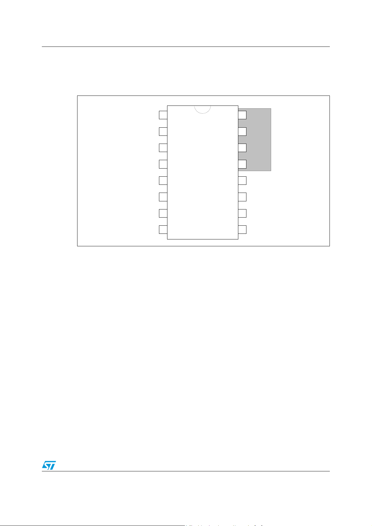
4 Pin connection
Figure 2. Pin connection (top view)
SOURCE
SOURCE
VCC
GND
ILED
DMG
COMP
N.A. N.A.
2
3
4
5
6
7
8
16
15
14
13
12
11
10
DRAIN1
DRAIN
DRAIN
DRAIN
N.C.
N.A.
N.A.
9
Note: The copper area for heat dissipation has to be designed under the drain pins
Doc ID 18077 Rev 1 7/29

Pin connection HVLED805
Table 5. Pin functions
N. Name Function
Power section source and input to the PWM comparator. The current flowing in the MOSFET
is sensed through a resistor connected between the pin and GND. The resulting voltage is
1, 2 SOURCE
3VCC
4GND
5ILED
6DMG
7COMP
8-11 N.A Not available. These pins must be left not connected
12 N.C Not internally connected. Provision for clearance on the PCB to meet safety requirements.
compared with an internal reference (0.75V typ.) to determine MOSFET’s turn-off. The pin is
equipped with 250 ns blanking time after the gate-drive output goes high for improved noise
immunity. If a second comparison level located at 1V is exceeded the IC is stopped and
restarted after Vcc has dropped below 5V.
Supply Voltage of the device. An electrolytic capacitor, connected between this pin and
ground, is initially charged by the internal high-voltage start-up generator; when the device is
running the same generator will keep it charged in case the voltage supplied by the auxiliary
winding is not sufficient. This feature is disabled in case a protection is tripped. Sometimes a
small bypass capacitor (100nF typ.) to GND might be useful to get a clean bias voltage for the
signal part of the IC.
Ground. Current return for both the signal part of the IC and the gate drive. All of the ground
connections of the bias components should be tied to a trace going to this pin and kept
separate from any pulsed current return.
CC regulation loop reference voltage. An external capacitor will be connected between this
pin and GND. An internal circuit develops a voltage on this capacitor that is used as the
reference for the MOSFET’s peak drain current during CC regulation. The voltage is
automatically adjusted to keep the average output current constant.
Transformer’s demagnetization sensing for quasi-resonant operation. Input/output voltage
monitor. A negative-going edge triggers MOSFET’s turn-on. The current sourced by the pin
during MOSFET’s ON-time is monitored to get an image of the input voltage to the converter,
in order to compensate the internal delay of the current sensing circuit and achieve a CC
regulation independent of the mains voltage. If this current does not exceed 50µA, either a
floating pin or an abnormally low input voltage is assumed, the device is stopped and
restarted after Vcc has dropped below 5V. Still, the pin voltage is sampled-and-held right at
the end of transformer’s demagnetization to get an accurate image of the output voltage to be
fed to the inverting input of the internal, transconductance-type, error amplifier, whose noninverting input is referenced to 2.5V. Please note that the maximum I
current has to not exceed ±2 mA (AMR) in all the Vin range conditions. No capacitor is
allowed between the pin and the auxiliary transformer.
Output of the internal transconductance error amplifier. The compensation network will be
placed between this pin and GND to achieve stability and good dynamic performance of the
voltage control loop.
sunk/sourced
DMG
Drain connection of the internal power section. The internal high-voltage start-up generator
13 to 16 DRAIN
8/29 Doc ID 18077 Rev 1
sinks current from this pin as well. Pins connected to the internal metal frame to facilitate heat
dissipation.
HVLED805 Pin connection
Figure 3. C
output capacitance variation
OSS
C
(pF)
OSS
500
400
300
200
100
0
0 25 50 75 100 125 150
(V)
V
DS
Figure 4. Off state drain and source current test circuit
DMG
Note: The measured I
µA typ. @ 750 V) and the effective MOSFET’s off state drain current
+
14V
-
VCC DRAIN
2.5V
is the sum between the current across the 12 MΩ start-up resistor (62.5
DSS
CUR RE NT
CONTROL
GND
S OUR CEIL EDCOM P
Idss
A
+
Vin
75 0V
Doc ID 18077 Rev 1 9/29

Pin connection HVLED805
μ
Figure 5. Start-up current test circuit
Icc start-up
2.5V
DMG
Figure 6. Quiescent current test circuit
+
A
11.8V
-
VCC DRAIN
CUR RE NT
CONTROL
S OUR CEIL EDCOM P
GND
Iq _m ea s
2.5V
DM G
33 k
3V
-
+
+
-
Iq = Iq_meas - - 100 A
A
VCC DRAIN
CUR RENT
CONTROL
0.1 1 3V
⋅
3.3kΩ
+
-
GND
14 V
SO URCEILE DCOMP
10k
+
-
0.2V0.8 V
10/29 Doc ID 18077 Rev 1

HVLED805 Pin connection
Figure 7. Operating supply current test circuit
+
15V
GND
10
50kHz
10k
A
27 k
220k
2.5V
DMG
10 k
+
-
-5V
Icc
VCC DRAIN
CU RRENT
CO NTRO L
2.8V
+
-
Note: The circuit across the DMG pin is used for switch-on synchronization
Figure 8. Quiescent current during fault test circuit
1.5k
2W
+
150V
-
S OU RCEIL EDCO MP
5.6
DMG
2.5V
Iq ( fa u l t )
+
A
14V
-
VCC DRAIN
CUR RE NT
CONTROL
S OUR CEIL EDCOM P
GND
Doc ID 18077 Rev 1 11/29

Application information HVLED805
5 Application information
The HVLED805 is an off-line all-primary sensing switching regulator, specific for offline LED
drivers based on quasi-resonant ZVS (zero voltage switching at switch turn-on) flyback
topology.
Depending on converter’s load condition, the device is able to work in different modes
(Figure 9 for constant voltage operation):
1. QR mode at heavy load. Quasi-resonant operation lies in synchronizing MOSFET's
turn-on to the transformer’s demagnetization by detecting the resulting negative-going
edge of the voltage across any winding of the transformer. Then the system works
close to the boundary between discontinuous (DCM) and continuous conduction
(CCM) of the transformer. As a result, the switching frequency will be different for
different line/load conditions (see the hyperbolic-like portion of the curves in Figure 9).
Minimum turn-on losses, low EMI emission and safe behavior in short circuit are the
main benefits of this kind of operation. The resulting constant current mode fixes the
average current also in case of a short-circuit failure of one or more LEDs.
2. Valley-skipping mode at medium/ light load. Depending on voltage on COMP pin, the
device defines the maximum operating frequency of the converter. As the load is
reduced MOSFET’s turn-on will not any more occur on the first valley but on the second
one, the third one and so on. In this way the switching frequency will no longer increase
(piecewise linear portion in Figure 9).
3. Burst-mode with no or very light load. When the load is extremely light or disconnected,
the converter will enter a controlled on/off operation with constant peak current.
Decreasing the load will then result in frequency reduction, which can go down even to
few hundred hertz, thus minimizing all frequency-related losses and making it easier to
comply with energy saving regulations or recommendations. Being the peak current
very low, no issue of audible noise arises. Thanks to this feature, the application is able
to safely manage the open circuit caused by an LED failure.
Figure 9. Multi-mode operation of HVLED805 (Constant voltage operation)
f
f
f
osc
osc
osc
f
f
f
sw
sw
sw
0
0
0
12/29 Doc ID 18077 Rev 1
Valley-skipping
Valley-skipping
Valley-skipping
mode
mode
mode
Burst-mode
Burst-mode
Burst-mode
Quasi-resonant mode
Quasi-resonant mode
Quasi-resonant mode
P
P
P
in
in
in
Input voltage
Input voltage
Input voltage
Pinmax
Pinmax
Pinmax

HVLED805 Application information
5.1 Power section and gate driver
The power section guarantees safe avalanche operation within the specified energy rating
as well as high dv/dt capability. The Power MOSFET has a V(BR)DSS of 800V min. and a
typical R
DSon
of 11 Ω.
The gate driver of the power MOSFET is designed to supply a controlled gate current during
both turn-on and turn-off in order to minimize common mode EMI. Under UVLO conditions
an internal pull-down circuit holds the gate low in order to ensure that the power MOSFET
cannot be turned on accidentally.
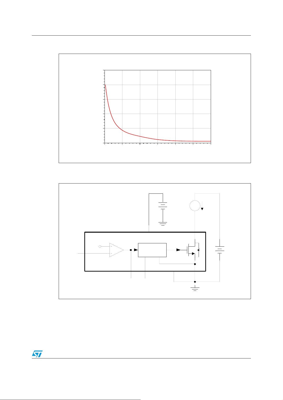
5.2 High voltage startup generator
Figure 10 shows the internal schematic of the high-voltage start-up generator (HV
generator). It includes an 800 V-rated N-channel MOSFET, whose gate is biased through
the series of a 12 MΩ resistor and a 14 V zener diode, with a controlled, temperaturecompensated current generator connected to its source. The HV generator input is in
common with the DRAIN pin, while its output is the supply pin of the device (Vcc). A mains
“UVLO” circuit (separated from the UVLO of the device that sense Vcc) keeps the HV
generator off if the drain voltage is below V
(50 V typical value).
START
Figure 10. High-voltage start-up generator: internal schematic
DR AI N
12 M14 V
Vcc_OK
Mai ns UV LO
CO NT RO L
HV_EN
IHV
Icharge
S OURCE
Vcc
With reference to the timing diagram of Figure 11, when power is applied to the circuit and
the voltage on the input bulk capacitor is high enough, the HV generator is sufficiently
biased to start operating, thus it will draw about 5.5 mA (typical) from the bulk capacitor.
Doc ID 18077 Rev 1 13/29

Application information HVLED805
Most of this current will charge the bypass capacitor connected between the Vcc pin and
ground and make its voltage rise linearly.
As the Vcc voltage reaches the start-up threshold (13 V typ.) the chip starts operating, the
internal power MOSFET is enabled to switch and the HV generator is cut off by the Vcc_OK
signal asserted high. The IC is powered by the energy stored in the Vcc capacitor.
The chip is able to power itself directly from the rectified mains: when the voltage on the V
pin falls below Vcc
generator is turned on and charges the supply capacitor until it reaches the V
(10.5V typ.), during each MOSFET’s off-time the HV current
restart
CCOn
CC
threshold.
In this way, the self-supply circuit develops a voltage high enough to sustain the operation of
the device. This feature is useful especially during CC regulation, when the flyback voltage
generated by the auxiliary winding alone may not be able to keep Vcc above V
CCrestart
.
At converter power-down the system will lose regulation as soon as the input voltage falls
below V
. This prevents converter’s restart attempts and ensures monotonic output
Start
voltage decay at system power-down.
Figure 11. Timing diagram: normal power-up and power-down sequences
Vin
Vin
Start
Start
V
V
Vcc
Vcc
VccON
VccON
Vccrestart
Vccrestart
DRAIN
DRAIN
t
t
t
t
Icharge
Icharge
5.5 mA
5.5 mA
Normal operation
Power-on
Power-on
Normal operation
CV mode
CV mode
14/29 Doc ID 18077 Rev 1
Normal operation
Normal operation
CC mode
CC mode
Power-o ff
Power-o ff
t
t
t
t
t
t
t
t

HVLED805 Application information
5.3 Secondary side demagnetization detection and triggering block
The demagnetization detection (DMG) and Triggering blocks switch on the power MOSFET
if a negative-going edge falling below 50 mV is applied to the DMG pin. To do so, the
triggering block must be previously armed by a positive-going edge exceeding 100 mV.
This feature is used to detect transformer demagnetization for QR operation, where the
signal for the DMG input is obtained from the transformer’s auxiliary winding used also to
supply the IC.
Figure 12. DMG block, triggering block
Rdmg
Aux
DMG
Rfb
110mV
60 mV
DMG
CLAMP
-
+
BLAN KI N G
TIME
Fr om C C/ CV Bl ock
TURN-ON
LO GI C
LE B
ST AR TE R
Fr om OCP
S
Q
R
To Dr iver
The triggering block is blanked after MOSFET’s turn-off to prevent any negative-going edge
that follows leakage inductance demagnetization from triggering the DMG circuit
erroneously.
This blanking time is dependent on the voltage on COMP pin: it is T
= 0.9 V, and decreases almost linearly down to T
BLANK
= 6 µs for V
BLANK
COMP
= 30 µs for V
= 1.3 V
COMP
The voltage on the pin is both top and bottom limited by a double clamp, as illustrated in the
internal diagram of the DMG block of Figure 12. The upper clamp is typically located at 3.3
V, while the lower clamp is located at -60mV. The interface between the pin and the auxiliary
winding will be a resistor divider. Its resistance ratio as well as the individual resistance
values will be properly chosen (see “Section 5.5: Constant current operation on page 18”
and “Section 5.6: Voltage feedforward block on page 20”.
Please note that the maximum I
sunk/sourced current has to not exceed ±2 mA (AMR)
DMG
in all the Vin range conditions. No capacitor is allowed between DMG pin and the auxiliary
transformer.
The switching frequency is top-limited below 166 kHz, as the converter’s operating
frequency tends to increase excessively at light load and high input voltage.
A Starter block is also used to start-up the system, that is, to turn on the MOSFET during
converter power-up, when no or a too small signal is available on the DMG pin.
The starter frequency is 2 kHz if COMP pin is below burst mode threshold, i.e. 1 V, while it
becomes 8 kHz if this voltage exceed this value.
Doc ID 18077 Rev 1 15/29

Application information HVLED805
V
After the first few cycles initiated by the starter, as the voltage developed across the auxiliary
winding becomes large enough to arm the DMG circuit, MOSFET’s turn-on will start to be
locked to transformer demagnetization, hence setting up QR operation.
The starter is activated also when the IC is in CC regulation and the output voltage is not
high enough to allow the DMG triggering.
If the demagnetization completes – hence a negative-going edge appears on the DMG pin –
after a time exceeding time T
from the previous turn-on, the MOSFET will be turned
BLANK
on again, with some delay to ensure minimum voltage at turn-on. If, instead, the negativegoing edge appears before T
going edge after T
will turn-on the MOSFET. In this way one or more drain ringing
BLANK
has elapsed, it will be ignored and only the first negative-
BLANK
cycles will be skipped (“valley-skipping mode”, Figure 13) and the switching frequency will
be prevented from exceeding 1/T
BLANK
.
Figure 13. Drain ringing cycle skipping as the load is progressively reduced
DS
V
DS
V
DS
T
T
FW
osc
T
V
Pin = Pin'
(limit condition)
T
ON
t
T
osc
in''
< P
in'
Pin= P
t
T
osc
in'''
Pin= P
< P
in''
Note: That when the system operates in valley skipping-mode, uneven switching cycles may be
observed under some line/load conditions, due to the fact that the OFF-time of the MOSFET
is allowed to change with discrete steps of one ringing cycle, while the OFF-time needed for
cycle-by-cycle energy balance may fall in between. Thus one or more longer switching
cycles will be compensated by one or more shorter cycles and vice versa. However, this
mechanism is absolutely normal and there is no appreciable effect on the performance of
the converter or on its output voltage.
5.4 Constant voltage operation
The IC is specifically designed to work in primary regulation and the output voltage is
sensed through a voltage partition of the auxiliary winding, just before the auxiliary rectifier
diode.
Figure 14 shows the internal schematic of the constant voltage mode and the external
connections.
t
16/29 Doc ID 18077 Rev 1

HVLED805 Application information
Figure 14. Voltage control principle: internal schematic
Rd mg
Aux
DMG
Rf b
S/ H
DEMAG
LO G I C
2.5V
-
EA
+
To PWM Logic
-
CV
+
From Rsense
COMP
R
C
Due to the parasitic wires resistance, the auxiliary voltage is representative of the output just
when the secondary current becomes zero. For this purpose, the signal on DMG pin is
sampled-and-held at the end of transformer’s demagnetization to get an accurate image of
the output voltage and it is compared with the error amplifier internal reference.
During the MOSFET’s OFF-time the leakage inductance resonates with the drain
capacitance and a damped oscillation is superimposed on the reflected voltage. The S/H
logic is able to discriminate such oscillations from the real transformer’s demagnetization.
When the DMG logic detects the transformer’s demagnetization, the sampling process
stops, the information is frozen and compared with the error amplifier internal reference.
The internal error amplifier is a transconductance type and delivers an output current
proportional to the voltage unbalance of the two outputs: the output generates the control
voltage that is compared with the voltage across the sense resistor, thus modulating the
cycle-by-cycle peak drain current.
The COMP pin is used for the frequency compensation: usually, an RC network, which
stabilizes the overall voltage control loop, is connected between this pin and ground.
The output voltage can be defined according the formula:
Equation 1
V
Where n
The R
DMG
AUX
SEC
REF
−⋅
SEC
and n
R ⋅
=
FB
n
n
are the secondary and auxiliary turn’s number respectively.
AUX
value can be defined depending on the application parameters (see “Section 5.6:
R
DMG
VV
REFOUT
Voltage feedforward block on page 20” section).
Doc ID 18077 Rev 1 17/29

Application information HVLED805
⋅
=
5.5 Constant current operation
Figure 15 presents the principle used for controlling the average output current of the
flyback converter.
The output voltage of the auxiliary winding is used by the demagnetization block to generate
the control signal for the mosfet switch Q1. A resistor R in series with it absorbs a current
/R, where VC is the voltage developed across the capacitor C.
V
C
The flip-flop’s output is high as long as the transformer delivers current on secondary side.
This is shown in
Figure 16.
The capacitor C has to be chosen so that its voltage V
Since it is charged and discharged by currents in the range of some ten µA (I
can be considered as a constant.
C
CLED
is
typically 20 µA) at the switching frequency rate, a capacitance value in the range 4.7-10 nF
is suited for switching frequencies in the ten kHz.
The average output current can be expressed as:
Equation 2
I
OUT
Where IS is the secondary peak current, T
⎛
⋅=
⎜
2
⎝
ONSEC
⎞
ONSECS
⎟
T
⎠
is the conduction time of the secondary
T
I
side and T is the switching period.
Taking into account the transformer ratio n between primary and secondary side, I
be expressed is a function of the primary peak current I
:
P
can also
S
Equation 3
InI
PS
As in steady state the average current IC:
Equation 4
()
⎛
ITTI
⎜
CLEDONSECCLED
⎝
Which can be solved for VC:
Equation 5
VV ⋅=
CLEDC
Where V
is fed to the CC comparator, the primary peak current can be expressed as:
As V
C
18/29 Doc ID 18077 Rev 1
CLED
=R • I
and is internally defined.
LED
−+−⋅
T
ONSEC
V
⎞
C
⎟
ONSEC
R
⎠
0T
=⋅
T

HVLED805 Application information
Equation 6
V
R
SENSE
C
I =
P
Combining (2), (3) (5) and (6):
Equation 7
n
I ⋅=
OUT
RV2
CLED
SENSE
This formula shows that the average output current does not depend anymore on the input
or the output voltage, neither on transformer inductance values. The external parameters
defining the output current are the transformer ratio n and the sense resistor R
SENSE
.
Figure 15. Current control principle
.
Iref
To PWM Logic
-
CC
+
R
From Rsense
Q1
Rdmg
DMG
DEMAG
LOGIC
S
Q
R
Aux
Rfb
ILED
CLED
Doc ID 18077 Rev 1 19/29

Application information HVLED805
⋅
Figure 16. Constant current operation: Switching cycle waveforms
T
I
P
t
Is
t
Q
t
I
IC
CLED
5.6 Voltage feedforward block
The current control structure uses the voltage VC to define the output current, according to
(7). Actually, the CC comparator will be affected by an internal propagation delay Td, which
will switch off the MOSFET with a peak current than higher the foreseen value.
This current overshoot will be equal to:
Equation 8
Will introduce an error on the calculated CC setpoint, depending on the input voltage.
The HVLED805 implements a Line Feedforward function, which solves the issue by
introducing an input voltage dependent offset on the current sense signal, in order to adjust
the cycle-by-cycle current limitation.
The internal schematic is shown in
Figure 17.
I −=
CLED
Δ I
P
VT
IN d
=
V
t
C
R
L
P
20/29 Doc ID 18077 Rev 1

HVLED805 Application information
(
Figure 17. Feedforward compensation: internal schematic
DRAIN
Rdmg
Aux
DMG
Rf b
Feedforward
Logi c
.
IF F
CC
Bl oc k
-
CC
+
PW M
LOGIC
RFF
SOURCE
Rs e n s e
During MOSFET’s ON-time the current sourced from DMG pin is mirrored inside the
“
Feedforward Logic” block in order to provide a feedforward current, I
FF
.
Such “feedforward current” is proportional to the input voltage according to the formula:
Equation 9
V
I⋅=
FF
IN
Rm
dmg
Where m is the primary-to-auxiliary turns ratio.
According to the schematic, the voltage on the non-inverting comparator will be:
Equation 10
(-)
V=R I+I R+R⋅⋅
SENSE D FF FF SENSE
)
The offset introduced by feedforward compensation will be:
Equation 11
V
IN
()
RR
SENSEFF
As RFF>>R
V +⋅
OFFSET
, the previous one can be simplified as:
SENSE
=
Rm
⋅
dmg
Equation 12
RV
⋅
V
OFFSET
=
FFIN
Rm
⋅
dmg
Doc ID 18077 Rev 1 21/29

Application information HVLED805
This offset is proportional to VIN and is used to compensate the current overshoot,
according to the formula:
Equation 13
TV
⋅
dIN
R
L
SENSE
p
RV
⋅
=⋅
FFIN
Rm
⋅
dmg
Finally, the R
resistor can be calculated as follows:
dmg
Equation 14
RL
N
R
dmg
N
AUX
PRI
⋅
⋅=
FFp
RT
⋅
SENSEd
In this case the peak drain current does not depend on input voltage anymore.
One more consideration concerns the R
sourced by the DMG pin, I
, is compared with an internal reference current I
DMG
value: during MOSFET’s ON-time, the current
dmg
µA typical).
If I
DMG
< I
DMGON
, the brownout function is activated and the IC is shut-down.
This feature is especially important when the auxiliary winding is accidentally disconnected
and considerably increases the end-product’s safety and reliability.
5.7 Burst-mode operation at no load or very light load
When the voltage at the COMP pin falls 65 mV below a threshold fixed internally at a value,
V
COMPBM
reduced at a lower value to minimize Vcc capacitor discharge.
In this condition the converter operates in burst-mode (one pulse train every T
µs), with minimum energy transfer.
, the IC is disabled with the MOSFET kept in OFF state and its consumption
DMGON
START
(-50
=500
As a result of the energy delivery stop, the output voltage decreases: after 500 µs the
controller switches-on the MOSFET again and the sampled voltage on the DMG pin is
compared with the internal reference. If the voltage on the EA output, as a result of the
comparison, exceeds the V
threshold, the device restarts switching, otherwise it stays
COMPL
OFF for another 500 µs period.
In this way the converter will work in burst-mode with a nearly constant peak current defined
by the internal disable level. A load decrease will then cause a frequency reduction, which
can go down even to few hundred hertz, thus minimizing all frequency-related losses and
making it easier to comply with energy saving regulations. This kind of operation, shown in
the timing diagrams of
Figure 19 along with the others previously described, is noise-free
since the peak current is low
22/29 Doc ID 18077 Rev 1

HVLED805 Application information
Figure 18. Load-dependent operating modes: timing diagrams
COMP
65 mV
hyster.
V
COMPL
DS
I
TSTART TSTART TSTART TSTART
5.8 Soft-start and starter block
The soft start feature is automatically implemented by the constant current block, as the
primary peak current will be limited from the voltage on the C
During start-up, as the output voltage is zero, the IC will start in CC mode with no high peak
current operations. In this way the voltage on the output capacitor will increase slowly and
the soft-start feature will be ensured.
Actually the C
value is not important to define the soft-start time, as its duration depends
LED
on others circuit parameters, like transformer ratio, sense resistor, output capacitors and
load. The user will define the best appropriate value by experiments.
5.9 Hiccup mode OCP
The device is also protected against short circuit of the secondary rectifier, short circuit on
the secondary winding or a hard-saturated flyback transformer. A comparator monitors
continuously the voltage on the R
exceeds 1 V.
SENSE
Normal-modeBurst-modeNormal-mode
capacitor.
LED
and activates a protection circuitry if this voltage
To distinguish an actual malfunction from a disturbance (e.g. induced during ESD tests), the
first time the comparator is tripped the protection circuit enters a “warning state”. If in the
subsequent switching cycle the comparator is not tripped, a temporary disturbance is
assumed and the protection logic will be reset in its idle state; if the comparator will be
tripped again a real malfunction is assumed and the device will be stopped.
This condition is latched as long as the device is supplied. While it is disabled, however, no
energy is coming from the self-supply circuit; hence the voltage on the V
capacitor will
CC
decay and cross the UVLO threshold after some time, which clears the latch. The internal
start-up generator is still off, then the V
Doc ID 18077 Rev 1 23/29
voltage still needs to go below its restart voltage
CC

Application information HVLED805
before the VCC capacitor is charged again and the device restarted. Ultimately, this will
result in a low-frequency intermittent operation (Hiccup-mode operation), with very low
stress on the power circuit. This special condition is illustrated in the timing diagram of
Figure 18.
Figure 19. Hiccup-mode OCP: timing diagram
VCC
VccON
VccOFF
Vccrest
VSOURC E
Vcsdis
VDS
1 V
Secondary diode is shorted here
5.10 Layout recommendations
A proper printed circuit board layout is essential for correct operation of any switch-mode
converter and this is true for the HVLED805 as well. Careful component placing, correct
traces routing, appropriate traces widths and compliance with isolation distances are the
major issues. In particular:
● The compensation network should be connected as close as possible to the COMP
pin, maintaining the trace for the GND as short as possible
● Signal ground should be routed separately from power ground, as well from the sense
resistor trace.
t
t
Two switching cycles
t
24/29 Doc ID 18077 Rev 1

HVLED805 Application information
Figure 20. Suggested routing for converter
ACIN
ACIN
VDD
DMG
COMP S OURCE
HVLED805
ILEDGND
DR AI N
LED
...
Doc ID 18077 Rev 1 25/29

Package mechanical data HVLED805
6 Package mechanical data
In order to meet environmental requirements, ST offers these devices in different grades of
ECOPACK
specifications, grade definitions and product status are available at: www.st.com.
ECOPACK
®
packages, depending on their level of environmental compliance. ECOPACK®
®
is an ST trademark.
Table 6. SO16N mechanical data
mm inch
Dim.
Min Typ Max Min Typ Max
A 1.75 0.069
a1 0.1 0.25 0.004 0.009
a2 1.6 0.063
b 0.35 0.46 0.014 0.018
b1 0.19 0.25 0.007 0.010
C 0.5 0.020
c1 45° (typ.)
D (1) 9.8 10 0.386 0.394
E 5.8 6.2 0.228 0.244
e 1.27 0.050
e3 8.89 0.350
F
(1) 3.8 4.0 0.150 0.157
G 4.60 5.30 0.181 0.208
L 0.4 1.27 0.150 0.050
M 0.62 0.024
S 8 °(max.)
26/29 Doc ID 18077 Rev 1

HVLED805 Package mechanical data
Figure 21. Package dimensions
Doc ID 18077 Rev 1 27/29

Revision history HVLED805
7 Revision history
Table 7. Document revision history
Date Revision Changes
14-Oct-2010 1 Initial release
28/29 Doc ID 18077 Rev 1

HVLED805
Please Read Carefully:
Information in this document is provided solely in connection with ST products. STMicroelectronics NV and its subsidiaries (“ST”) reserve the
right to make changes, corrections, modifications or improvements, to this document, and the products and services described herein at any
time, without notice.
All ST products are sold pursuant to ST’s terms and conditions of sale.
Purchasers are solely responsible for the choice, selection and use of the ST products and services described herein, and ST assumes no
liability whatsoever relating to the choice, selection or use of the ST products and services described herein.
No license, express or implied, by estoppel or otherwise, to any intellectual property rights is granted under this document. If any part of this
document refers to any third party products or services it shall not be deemed a license grant by ST for the use of such third party products
or services, or any intellectual property contained therein or considered as a warranty covering the use in any manner whatsoever of such
third party products or services or any intellectual property contained therein.
UNLESS OTHERWISE SET FORTH IN ST’S TERMS AND CONDITIONS OF SALE ST DISCLAIMS ANY EXPRESS OR IMPLIED
WARRANTY WITH RESPECT TO THE USE AND/OR SALE OF ST PRODUCTS INCLUDING WITHOUT LIMITATION IMPLIED
WARRANTIES OF MERCHANTABILITY, FITNESS FOR A PARTICULAR PURPOSE (AND THEIR EQUIVALENTS UNDER THE LAWS
OF ANY JURISDICTION), OR INFRINGEMENT OF ANY PATENT, COPYRIGHT OR OTHER INTELLECTUAL PROPERTY RIGHT.
UNLESS EXPRESSLY APPROVED IN WRITING BY AN AUTHORIZED ST REPRESENTATIVE, ST PRODUCTS ARE NOT
RECOMMENDED, AUTHORIZED OR WARRANTED FOR USE IN MILITARY, AIR CRAFT, SPACE, LIFE SAVING, OR LIFE SUSTAINING
APPLICATIONS, NOR IN PRODUCTS OR SYSTEMS WHERE FAILURE OR MALFUNCTION MAY RESULT IN PERSONAL INJURY,
DEATH, OR SEVERE PROPERTY OR ENVIRONMENTAL DAMAGE. ST PRODUCTS WHICH ARE NOT SPECIFIED AS "AUTOMOTIVE
GRADE" MAY ONLY BE USED IN AUTOMOTIVE APPLICATIONS AT USER’S OWN RISK.
Resale of ST products with provisions different from the statements and/or technical features set forth in this document shall immediately void
any warranty granted by ST for the ST product or service described herein and shall not create or extend in any manner whatsoever, any
liability of ST.
ST and the ST logo are trademarks or registered trademarks of ST in various countries.
Information in this document supersedes and replaces all information previously supplied.
The ST logo is a registered trademark of STMicroelectronics. All other names are the property of their respective owners.
© 2010 STMicroelectronics - All rights reserved
STMicroelectronics group of companies
Australia - Belgium - Brazil - Canada - China - Czech Republic - Finland - France - Germany - Hong Kong - India - Israel - Italy - Japan -
Malaysia - Malta - Morocco - Philippines - Singapore - Spain - Sweden - Switzerland - United Kingdom - United States of America
www.st.com
Doc ID 18077 Rev 1 29/29
 Loading...