

查询HMC335G16供应商
MICROWAVE CORPORATION
Typical Applications
The HMC335G16 is ideal for:
• T elecom Infrastructure
9
• Military Radios, Radar & ECM
• Space Applications
• T est Instrumentation
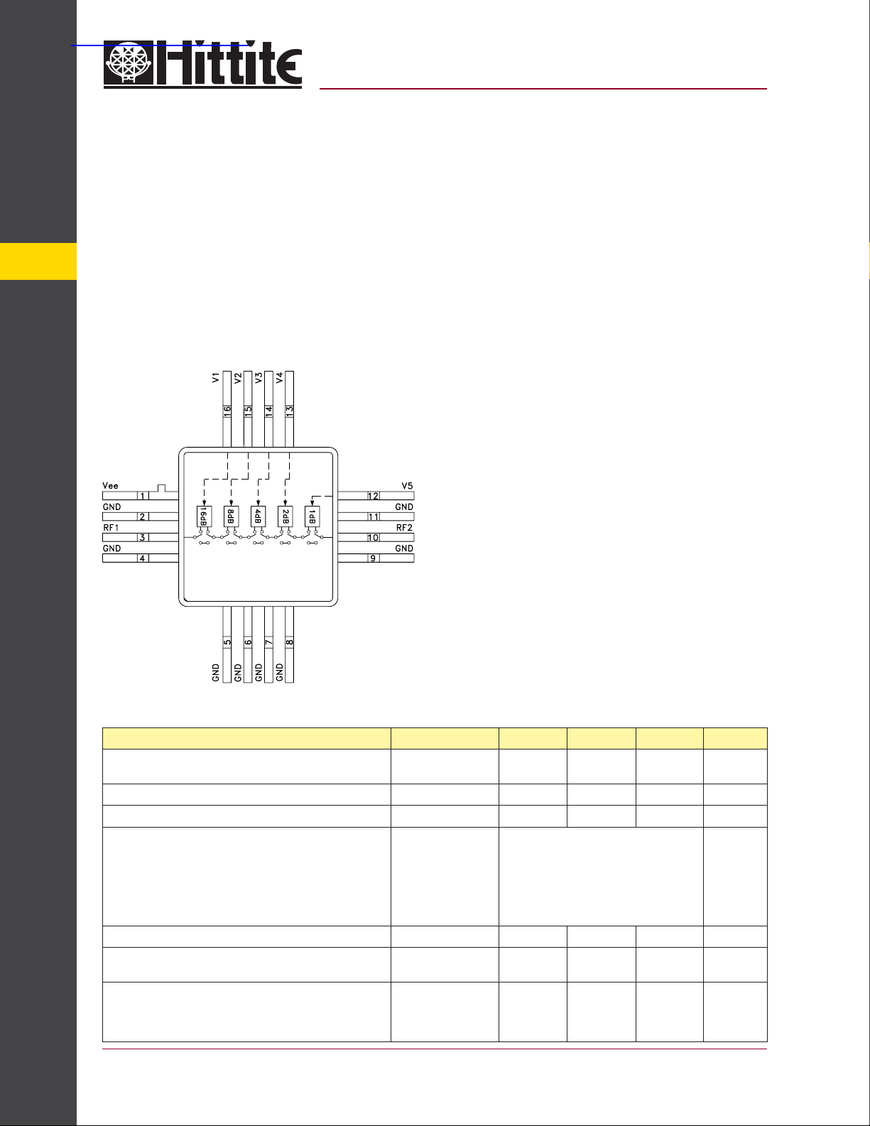
Functional Diagram
ATTENUATORS - SMT
v00.1102
HMC335G16
1dB LSB GaAs MMIC 5-BIT DIGITAL
ATTENUATOR, DC - 3 GHz
Features
1 dB LSB Steps to 31 dB
Single Control Line Per Bit
+/- 0.5 dB Typical Bit Error
16 Lead Hermetic SMT Package
General Description
The HMC335G16 is a broadband 5-bit GaAs IC
digital attenuator in a 16 lead glass/metal (hermetic)
surface mount package. Cov ering DC to 3 GHz, the
insertion loss is less than 2.3 dB typical. The attenuator bit values are 1 (LSB), 2, 4, 8, and 16 dB for
a total attenuation of 31 dB. Attenuation accuracy
is excellent at ±0.5 dB typical with an IIP3 of up to
+44 dBm. Five bit control voltage inputs, toggled
between 0 and -5V, are used to select each attenuation state at less than 70 µA each. A single V ee bias
of -5V allows operation down to DC.
9 - 56
Electrical Specifi cations, T
Parameter Frequency Min. Typical Max. Units
Insertion Loss DC - 1.5 GHz
Attenuation Range DC - 3.0 GHz 31 dB
Return Loss (RF1 & RF2, All Atten. States) DC - 3.0 GHz 13 dB
Attenuation Accuracy: (Referenced to Insertion Loss)
1 - 31 dB States
1 - 27 dB States
28 - 31 dB States
1 - 23 dB States
24 - 27 dB States
28 - 31 dB States
Input Power for 0.1 dB Compression 0.5 - 3.0 GHz 24 dBm
Input Third Order Intercept Point
(Two-tone Input Power = 0 dBm Each Tone)
Switching Characteristics
tRISE, tFALL (10/90% RF)
tON, tOFF (50% CTL to 10/90% RF)
For price, delivery, and to place orders, please contact Hittite Microwave Corporation:
12 Elizabeth Drive, Chelmsford, MA 01824 Phone: 978-250-3343 Fax: 978-250-3373
= +25° C, Vee = -5V & Vctl = 0/Vee
A
1.5 - 3.0 GHz
DC - 1.0 GHz
1.0 - 2.0 GHz
1.0 - 2.0 GHz
2.0 - 3.0 GHz
2.0 - 3.0 GHz
2.0 - 3.0 GHz
0.5 - 3.0 GHz 44 dBm
DC - 3.0 GHz
Order Online at www.hittite.com
± 0.3 + 5% of Atten. Setting Max
± 0.3 + 5% of Atten. Setting Max
± 0.3 + 8% of Atten. Setting Max
± 0.3 + 5% of Atten. Setting Max
± 0.3 + 8% of Atten. Setting Max
± 0.5 + 10% of Atten. Setting Max
2.0
2.3
140
160
2.5
2.8
dB
dB
dB
dB
dB
dB
dB
dB
ns
ns
MICROWAVE CORPORATION
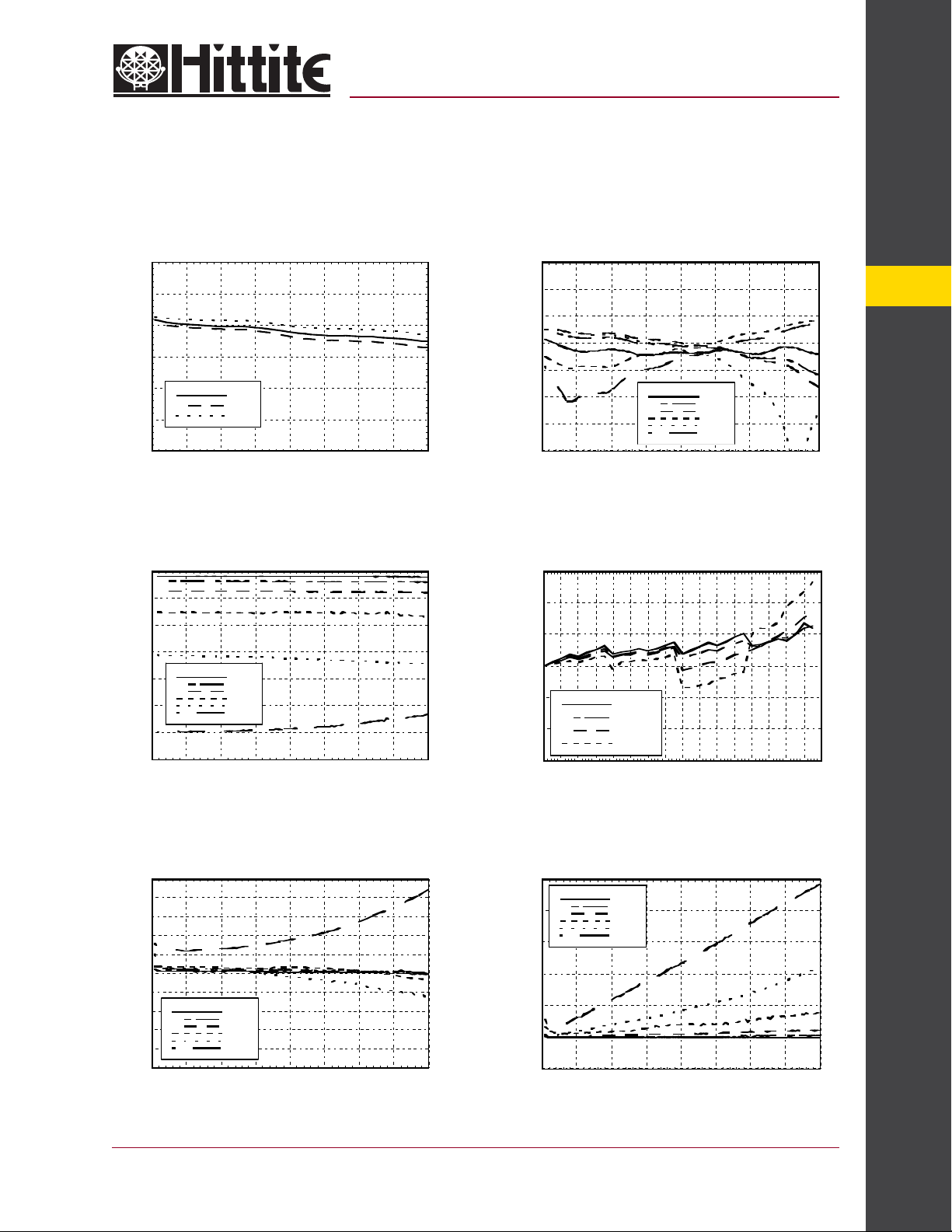
Insertion Loss
v00.1102
HMC335G16
1dB LSB GaAs MMIC 5-BIT DIGITAL
ATTENUATOR, DC - 3 GHz
Return Loss RF1, RF2
(Only Major States are Shown)
0
-1
-2
-3
-4
INSERTION LOSS (dB)
-5
-6
0 0.5 1 1.5 2 2.5 3 3.5 4
+25C
+85C
-40C
FREQUENCY (GHz)
Normalized Attenuation
(Only Major States are Shown)
0
-5
-10
-15
-20
-25
-30
NORMALIZED ATTENUATION (dB)
-35
0 0.5 1 1.5 2 2.5 3 3.5 4
1 dB
2 dB
4 dB
8 dB
16 dB
31 dB
FREQUENCY (GHz)
0
-5
-10
-15
-20
-25
RETURN LOSS (dB)
-30
-35
0 0.5 1 1.5 2 2.5 3 3.5 4
FREQUENCY (GHz)
1 dB
2 dB
4 dB
8 dB
16 dB
31 dB
Bit Error
vs. Attenuation State
3
2
1
0
-1
BIT ERROR (dB)
-2
-3
0 2 4 6 8 10 12 14 16 18 20 22 24 26 28 30 32
0.12 GHz
1.0 GHz
2.0 GHz
3.0 GHz
ATTENUATION STATE (dB)
9
ATTENUATORS - SMT
Bit Error vs. Frequency
(Only Major States are Shown)
5
4
3
2
1
0
-1
BIT ERROR (dB)
-2
-3
-4
-5
0 0.5 1 1.5 2 2.5 3 3.5 4
1 dB
2 dB
4 dB
8 dB
16 dB
31 dB
FREQUENCY (GHz)
For price, delivery, and to place orders, please contact Hittite Microwave Corporation:
12 Elizabeth Drive, Chelmsford, MA 01824 Phone: 978-250-3343 Fax: 978-250-3373
Relative Phase vs. Frequency
(Only Major States are Shown)
100
80
60
40
20
RELATVIE PHASE (deg)
0
-20
0 0.5 1 1.5 2 2.5 3 3.5 4
Order Online at www.hittite.com
1 dB
2 dB
4 dB
8 dB
16 dB
31 dB
FREQUENCY (GHz)
9 - 57

MICROWAVE CORPORATION
v00.1102
1dB LSB GaAs MMIC 5-BIT DIGITAL
ATTENUATOR, DC - 3 GHz
Worst Case Step Error
Between Successive Attenuation States
3
HMC335G16
9
Bias Voltage & Current
ATTENUATORS - SMT
Control V oltage
Note: Vee = -5V
Absolute Maximum Ratings
Control Voltage (V1 - V5) Vee - 0.5 Vdc
Bias Voltage (V ee) -7.0 Vdc
Storage Temperature -65 to +150 °C
Operating Temperature -40 to +85 °C
RF Input Power (0.5 - 3 GHz) +26 dBm
2
1
0
-1
STEP ERROR (dB)
-2
-3
0 0.5 1 1.5 2 2.5 3 3.5 4
Vee Range = -5.0 Vdc ± 10%
Vee (VDC) lee (Typ.) (mA) lee (Max.) (mA)
-5.0 3 6
State Bias Condition
Low 0 to -2V @ 70 µA Typ.
High Vee to Vee + 0.8V @ 5 µA Typ.
± 10%
FREQUENCY (GHz)
T ruth T able
16 dBV28 dBV34 dBV42 dBV51 dB
Any combination of the above states will provide an attenuation
approximately equal to the sum of the bits selected.
Control Voltage Input
V1
Low Low Low Low Low Reference I.L.
Low Low Low Low High 1 dB
Low Low Low High Low 2 dB
Low Low High Low Low 4 dB
Low High Low Low Low 8 dB
High Low Low Low Low 16 dB
High High High High High
Attenuation
State
RF1 - RF2
31 dB
Max. Atten.
9 - 58
For price, delivery, and to place orders, please contact Hittite Microwave Corporation:
12 Elizabeth Drive, Chelmsford, MA 01824 Phone: 978-250-3343 Fax: 978-250-3373
Order Online at www.hittite.com

MICROWAVE CORPORATION
Outline Drawing
v00.1102
HMC335G16
1dB LSB GaAs MMIC 5-BIT DIGITAL
ATTENUATOR, DC - 3 GHz
9
NOTES:
1. PACKAGE MATERIAL: ALUMINA LOADED BOROSILICATE GLASS.
2. LEADS, BASE, COVER MATEIRAL: KOVARTM (#7052 CORNING).
3. PLATING: ELECTROLYTIC GOLD 50 MICROINCHES MIN.,
OVER ELECTROLYTIC NICKEL 75 MICROINCHES MIN.
4. ALL DIMENSIONS ARE IN INCHES [MILLIMETERS].
5. TOLERANCES: 0.005 [.013] UNLESS OTHERWISE SPECIFIED.
6. CHARACTERS TO BE HELVETICA MEDIUM .030 HIGH,
BLACK INK, LOCATED APPROX. AS SHOWN.
7. ALL GROUND LEADS AND GROUND PADDLE MUST BE SOLDERED
TO PCB RF GROUND.
Pin Descriptions
Pin Number Function Description Interface Schematic
1 V ee Supply Voltage -5V ±10%
2, 4-9, 11 GND Package bottom must also be connected to RF ground.
3, 10 RF1, RF2
12-16 V1-V5 See truth table and control voltage table.
These pins are DC coupled and matched to 50 Ohm.
Blocking capacitors are required.
ATTENUATORS - SMT
For price, delivery, and to place orders, please contact Hittite Microwave Corporation:
12 Elizabeth Drive, Chelmsford, MA 01824 Phone: 978-250-3343 Fax: 978-250-3373
Order Online at www.hittite.com
9 - 59

9
MICROWAVE CORPORATION
Application Circuit
v00.1102
HMC335G16
1dB LSB GaAs MMIC 5-BIT DIGITAL
ATTENUATOR, DC - 3 GHz
DC Blocking Capacitors C1 & C2 are required on RF1 & RF2. Choose C1 = C2 = 100 pF ~ 0.1 uF to allow lowest customer
ATTENUATORS - SMT
specifi c frequency to pass with minimal loss. R1= 5K Ohm is required to supply voltage to the circuit through either Pin 3 or
Pin 10.
Suggested Driver Circuit
(One Circuit Required Per Bit Control Input)
Simple driver using inexpensive standard logic ICs pro vides f ast s witching using minimum DC current. * Recommended value
to suppress unwanted RF signals at V1 - V5 control lines.
9 - 60
For price, delivery, and to place orders, please contact Hittite Microwave Corporation:
12 Elizabeth Drive, Chelmsford, MA 01824 Phone: 978-250-3343 Fax: 978-250-3373
Order Online at www.hittite.com

MICROWAVE CORPORATION
Evaluation PCB
v00.1102
HMC335G16
1dB LSB GaAs MMIC 5-BIT DIGITAL
ATTENUATOR, DC - 3 GHz
9
List of Material
Item Description
J1 - J2 PC Mount SMA Connector
J3 DC Connector
R1 5k Ohm Resistor 0402 Pkg.
R2 - R6 100 Ohm Resistor, 0402 Pkg.
C1, C2
C3 1000pF Capacitor, 0603 Pkg.
U1 HMC335G16 Digital Attenuator
PCB* 106467 Evaluation PCB
*Circuit Board Material: Rogers 4350
0402 Chip Capacitor,
Select Value for Lowest Frequency of Operation
* R2 - R6 = 100 Ohm.
These resistors are optional and may be
used to enhance decoupling of the RF
path from the control inputs.
ATTENUATORS - SMT
The circuit board used in the fi nal application should use RF circuit design techniques. Signal lines should have 50 ohm impedance while the package ground leads and package bottom
should be connected directly to the ground plane similar to that
shown. A suffi cient number of via holes should be used to connect the top and bottom ground planes. The evaluation circuit
board shown is available from Hittite upon request.
For price, delivery, and to place orders, please contact Hittite Microwave Corporation:
12 Elizabeth Drive, Chelmsford, MA 01824 Phone: 978-250-3343 Fax: 978-250-3373
Order Online at www.hittite.com
9 - 61
 Loading...