

查询HMC333供应商
12
MICROWAVE CORPORATION
Typical Applications
The HMC333 is ideal for:
• Wireless Local Loop
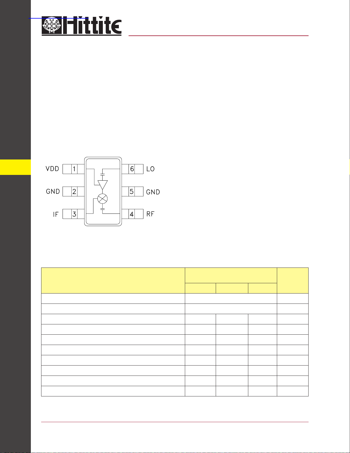
Functional Diagram
v00.0901
HMC333
GaAs MMIC MIXER w/ INTEGRATED
LO AMPLIFIER, 3.0 - 3.8 GHz
Features
Integrated LO Amplifi er w/ Pdiss: < 25 mW
Conversion Loss / Noise Figure: 8.5 dB
Low LO Drive Level: 0 dBm
Input IP3: +10 dBm
Single Positive Supply: 3V to 5V
General Description
The HMC333 is a single balanced mixer IC with an
integrated LO amplifi er. This converter IC can operate as an upconverter or downconverter between
3.0 GHz and 3.8 GHz. With the integrated LO amplifi er, the mixer requires an LO drive level of only 0
dBm, and requires only 7 mA from a single positive
+3V rail. The mixer has 8.5 dB of conversion loss,
an input P1dB of 0 dBm and an input third order
intercept point of +10 dBm at 3.5 GHz.
MIXERS - SMT
Electrical Specifi cations, T
Frequency Range, RF & LO 3.0 - 3.8 GHz
Frequency Range, IF DC - 1.0 GHz
Conversion Loss 8.5 11 dB
Noise Figure (SSB) 8.5 11 dB
LO to RF Isolation 10 15 dB
LO to IF Isolation 5 10 dB
RF to IF Isolation 10 15 dB
IP3 (Input) 3 10 dBm
1 dB Compression (Input) -3 +1 dBm
Supply Current (Idd) 7mA
* Unless otherwise noted, all measurements performed as downconverter, IF= 100 MHz.
Parameter
= +25° C
A
IF = 100 MHz
LO = 0 dBm & Vdd = +3V
Min. Typ. Max.
Units
12 - 154
For price, delivery, and to place orders, please contact Hittite Microwave Corporation:
12 Elizabeth Drive, Chelmsford, MA 01824 Phone: 978-250-3343 Fax: 978-250-3373
Order Online at www.hittite.com
MICROWAVE CORPORATION
v00.0901
HMC333
GaAs MMIC MIXER w/ INTEGRATED
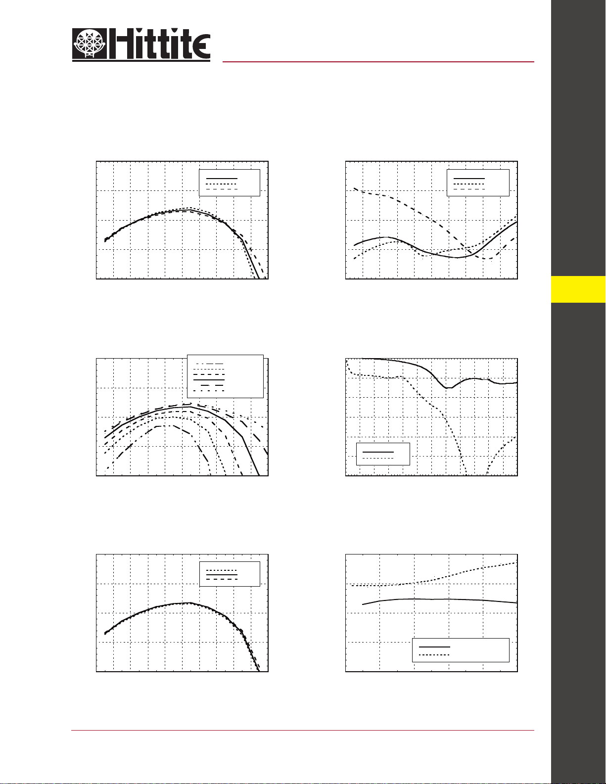
Conversion Gain vs.
Temperature @ LO = 0 dBm
0
-5
-10
-15
CONVERSION GAIN (dB)
-20
2.4 2.6 2.8 3 3.2 3.4 3.6 3.8 4 4.2 4.4
FREQUENCY (GHz)
0
-5
+25 C
-40 C
+85 C
LO = -6dBm
LO = -4dBm
LO = -2dBm
LO = 0dBm
LO = +2dBm
LO = +4dBm
LO AMPLIFIER, 3.0 - 3.8 GHz
Isolation @ LO = 0 dBm
0
RF/IF
LO/RF
-5
-10
ISOLATION (dB)
-15
-20
2.4 2.6 2.8 3 3.2 3.4 3.6 3.8 4 4.2 4.4
FREQUENCY (GHz)
Return Loss @ LO = 0 dBmConversion Gain vs. LO Drive
0
-5
-10
LO/IF
12
-10
-15
CONVERSION GAIN (dB)
-20
2.4 2.6 2.8 3 3.2 3.4 3.6 3.8 4 4.2 4.4
FREQUENCY (GHz)
Conversion Gain vs. Vdd @ LO = 0 dBm
0
+2.7V
+3.0V
-5
-10
-15
CONVERSION GAIN (dB)
-20
2.4 2.6 2.8 3 3.2 3.4 3.6 3.8 4 4.2 4.4
FREQUENCY (GHz)
+3.3V
-15
-20
RETURN LOSS (dB)
-25
-30
0 0.5 1 1.5 2 2.5 3 3.5 4 4.5 5 5.5 6
RF
LO
FREQUENCY (GHz)
IF Bandwidth @ LO = 0 dBm
0
-5
-10
RESPONSE (dB)
-15
-20
0 0.2 0.4 0.6 0.8 1
FREQUENCY (GHz)
CONVERSION GAIN
RETURN LOSS
MIXERS - SMT
For price, delivery, and to place orders, please contact Hittite Microwave Corporation:
12 Elizabeth Drive, Chelmsford, MA 01824 Phone: 978-250-3343 Fax: 978-250-3373
Order Online at www.hittite.com
12 - 155

MICROWAVE CORPORATION
v00.0901
HMC333
GaAs MMIC MIXER w/ INTEGRATED
12
Upconverter Performance
Conversion Gain @ LO = 0 dBm
0
-5
-10
-15
CONVERSION GAIN (dB)
-20
3 3.2 3.4 3.6 3.8 4
FREQUENCY (GHz)
Input IP3 vs. LO Drive*
20
15
-2 dBm
0 dBm
+2 dBm
LO AMPLIFIER, 3.0 - 3.8 GHz
Input P1dB vs.
Temperature @ LO = 0 dBm
10
8
6
4
2
0
-2
-4
INPUT P1dB (dBm)
-6
-8
-10
2.9 3 3.1 3.2 3.3 3.4 3.5 3.6 3.7 3.8 3.9
FREQUENCY (GHz)
Input IP3 vs.
Temperature @ LO = 0 dBm*
20
15
+25 C
-40 C
+85 C
+25 C
-40 C
+85 C
10
INPUT IP3 (dBm)
5
MIXERS - SMT
0
3 3.1 3.2 3.3 3.4 3.5 3.6 3.7 3.8 3.9 4
Input IP3 vs. Vdd @ LO = 0 dBm*
20
15
10
INPUT IP3 (dBm)
5
0
3 3.1 3.2 3.3 3.4 3.5 3.6 3.7 3.8 3.9 4
FREQUENCY (GHz)
FREQUENCY (GHz)
+2.7V
+3.0V
+3.3V
10
INPUT IP3 (dBm)
5
0
3 3.1 3.2 3.3 3.4 3.5 3.6 3.7 3.8 3.9 4
FREQUENCY (GHz)
Input P1dB vs. Vdd @ LO = 0 dBm
10
8
6
4
2
0
-2
-4
INPUT P1dB (dBm)
-6
-8
-10
2.9 3 3.1 3.2 3.3 3.4 3.5 3.6 3.7 3.8 3.9
FREQUENCY (GHz)
+2.7V
+3.0V
+3.3V
12 - 156
* Two-tone input power= -10 dBm each tone, 1 MHz spacing.
For price, delivery, and to place orders, please contact Hittite Microwave Corporation:
12 Elizabeth Drive, Chelmsford, MA 01824 Phone: 978-250-3343 Fax: 978-250-3373
Order Online at www.hittite.com

MICROWAVE CORPORATION
v00.0901
HMC333
GaAs MMIC MIXER w/ INTEGRATED
MxN Spurious @ IF Port
nLO
mRF01234
0xx-9-51234
1 8 0 32 25 34
2 3349404043
3 6856684872
4 7780798071
RF = 3.5 GHz @ -10 dBm
LO = 3.4 GHz @ 0 dBm
All values in dBc below IF power level.
Absolute Maximum Ratings
RF / IF Input (Vdd = +3V) +13 dBm
LO Drive (Vdd = +3V) +13 dBm
Vdd 5.5V
Continuous Pdiss (Ta = 85 °C)
(derate 2.64 mW/°C above 85 °C)
IF DC Current ±3 mA
Storage Temperature -65 to +150 °C
Operating Temperature -40 to +85 °C
238 mW
LO AMPLIFIER, 3.0 - 3.8 GHz
Harmonics of LO
nLO Spur @ RF Port
LO Freq. (GHz) 1 2 3 4
3 12 8 16 49
3.17 13 8 20 39
3.34 17 10 22 42
3.51 15 14 26 48
3.68 14 17 25 42
3.85 14 18 22 43
LO = 0 dBm
All values in dBc below input LO level @ RF port.
12
Outline Drawing
MIXERS - SMT
NOTES:
1. PACKAGE BODY MATERIAL: LOW STRESS INJECTION MOLDED
PLASTIC SILICA AND SILICON IMPREGNATED.
2. LEADFRAME MATERIAL: COPPER ALLOY
3. LEADFRAME PLATING: Sn/Pb SOLDER
4. DIMENSIONS ARE IN INCHES [MILLIMETERS].
5. DIMENSION DOES NOT INCLUDE MOLDFLASH OF 0.15mm PER SIDE.
6. DIMENSION DOES NOT INCLUDE MOLDFLASH OF 0.25mm PER SIDE.
7. ALL GROUND LEADS MUST BE SOLDERED TO PCB RF GROUND.
For price, delivery, and to place orders, please contact Hittite Microwave Corporation:
12 Elizabeth Drive, Chelmsford, MA 01824 Phone: 978-250-3343 Fax: 978-250-3373
Order Online at www.hittite.com
12 - 157

MICROWAVE CORPORATION
v00.0901
HMC333
GaAs MMIC MIXER w/ INTEGRATED
12
LO AMPLIFIER, 3.0 - 3.8 GHz
Pin Descriptions
Pin Number Function Description Interface Schematic
1 Vdd
2, 5 GND Ground: Pin must connect to RF ground.
3 IF Port
4 RF Port
Power supply for the LO Amplifi er. Two external RF bypass
capacitors (10 pF & 10,000 pF) and an external inductor (1.8
nH) are required.
IF Port: This pin is DC coupled. For applications not requiring
operation to DC, this port should be DC blocked externally
using a series capacitor whose value has been chosen to pass
the necessary IF frequency range. For operation to DC, this pin
must not source/sink more than 3mA of current or die non-func-
tion and possible die failure will result.
RF Port: This pin is AC coupled and matched to 50 Ohm from
3.0 - 3.8 GHz.
MIXERS - SMT
Application Circuit
12 - 158
6 LO Port
For price, delivery, and to place orders, please contact Hittite Microwave Corporation:
12 Elizabeth Drive, Chelmsford, MA 01824 Phone: 978-250-3343 Fax: 978-250-3373
LO Port: This pin is AC coupled and matched to 50 Ohm from
3.0 - 3.8 GHz
Order Online at www.hittite.com

MICROWAVE CORPORATION
v00.0901
HMC333
GaAs MMIC MIXER w/ INTEGRATED
Evaluation PCB
LO AMPLIFIER, 3.0 - 3.8 GHz
12
List of Materials
Item Description
J1 - J4 PC Mount SMA RF Connector
C1 10 pF Capacitor, 0603 Pkg.
C2 .01 µF Capacitor, 0603 Pkg.
L1 1.8 nH Inductor, 0805 Pkg.
U1 HMC333 Mixer
PCB* 103927 Evaluation Board
* Circuit Board Material: Rogers 4350
For price, delivery, and to place orders, please contact Hittite Microwave Corporation:
12 Elizabeth Drive, Chelmsford, MA 01824 Phone: 978-250-3343 Fax: 978-250-3373
Order Online at www.hittite.com
MIXERS - SMT
The circuit board used in the fi nal application should use
RF circuit design techniques. Signal lines should have
50 ohm impedance while the package ground leads
should be connected directly to the ground plane similar
to that shown. A suffi cient number of VIA holes should
be used to connect the top and bottom ground planes.
The evaluation circuit board shown is available from Hittite upon request.
12 - 159
 Loading...