

HCF4556B
DUAL BINARY TO 1 OF 4 DECODER/DEMULTIPLEXER
OUTPUT LOW ON SELECT
■ EXPANDABLE WITH MULTIPLE PACKAGES
■ STANDARDIZED SYMMETRICAL OUTPUT
CHARACTERISTICS
■ QUIESCENT CURRENT SPECIFIED UP TO
20V
■ 5V, 10V AND 15V PARAMETRIC RAT INGS
■ INPUT LEAKAGE CURRENT
I
= 100nA (MAX) AT VDD = 18V TA = 25°C
I
■ 100% TESTED FOR QUIESCENT CURRENT
■
MEETS ALL REQUIREMENTS OF JEDEC
JESD13B " STANDARD SPECIF ICATIONS
FOR DESCRIPTI ON OF B SERI ES CMOS
DEVICES"
DESCRIPTION
The HCF4556B is a m onolithic integrated circuit
fabricated in Metal Oxide Semiconductor
technology available in DIP and SOP packages.
The HCF4556B is a dual 1 of 4 decoder/
demultiplexer. Each decoder has two select inputs
(A and B), an Enabl e input (E
), and four mutually
DIP SOP
ORDER CODES
PACKAGE TUBE T & R
DIP HCF4556BEY
SOP HCF4556BM1 HCF4556M013TR
exclusive outputs. O n the HCF4556B the ou tputs
are low on select. When the Enable input is high,
the outputs is high regardless of the state of the
select inputs A and B.
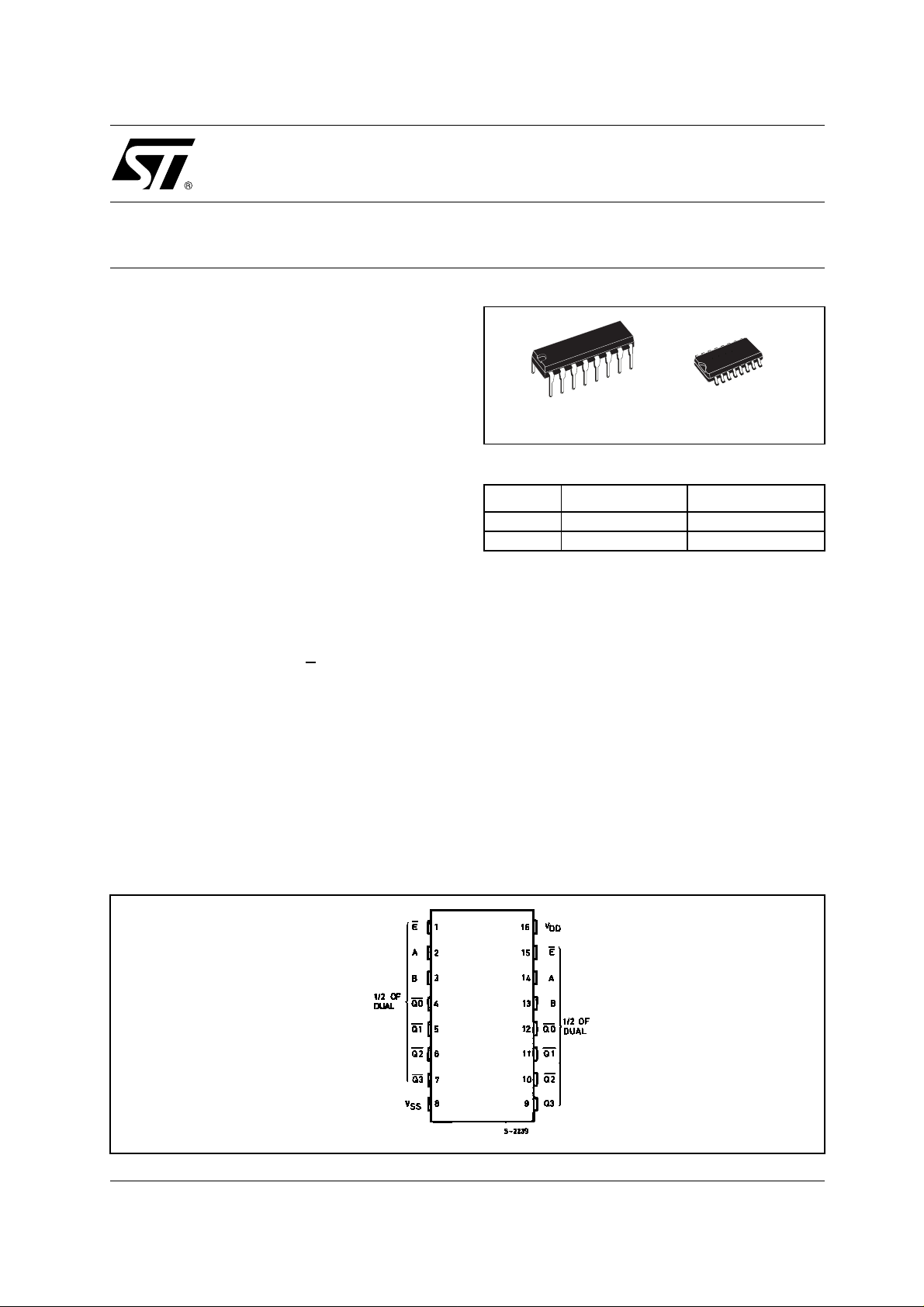
PIN CONNECTION
1/9September 2001
HCF4556B
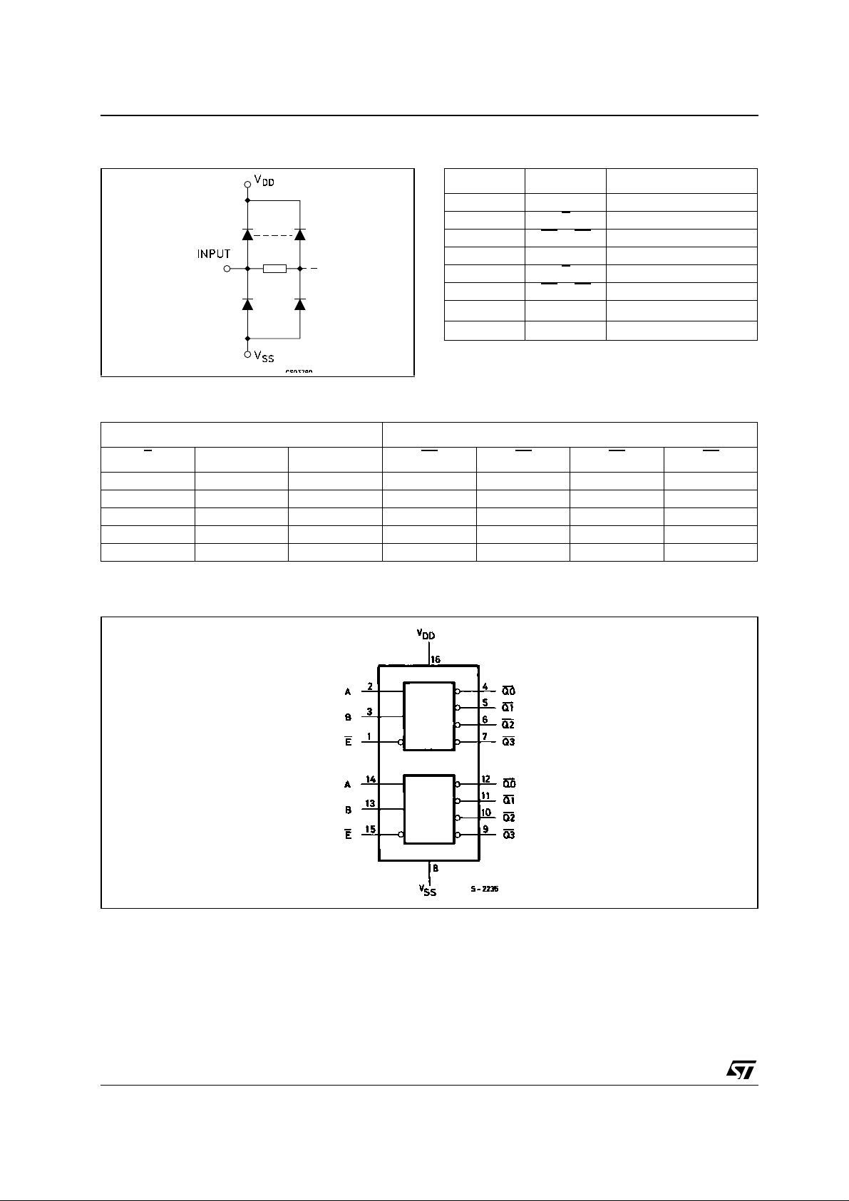
IINPUT EQUIVALENT CIRCUIT PIN DESCRIPTION
PIN No SYMBOL NAME AND FUNCTION
2, 3 A, B Select Inputs (1/2 of dual)
1E
4, 5, 6, 7 Q0
14, 13 A, B Select Inputs (1/2 of dual)
15 E
12, 1 1, 10, 9 Q0
8
16
TRUTH TABLE
INPUTS ENABLE SELECT OUTPUTS
to Q3 Outputs (1/2 of dual)
to Q3 Outputs (1/2 of dual)
V
SS
V
DD
Enable Input (1/2 of dual)
Enable Input (1/2 of dual)
Negative Supply Voltage
Positive Supply Voltage
E
LLLHHHL
LLHHHLH
LHLHLHH
LHHLHHH
HXXHHHH
X : Don’t Care
BAQ3Q2 Q1 Q0
FUNCTIONAL DIAGRAM
2/9
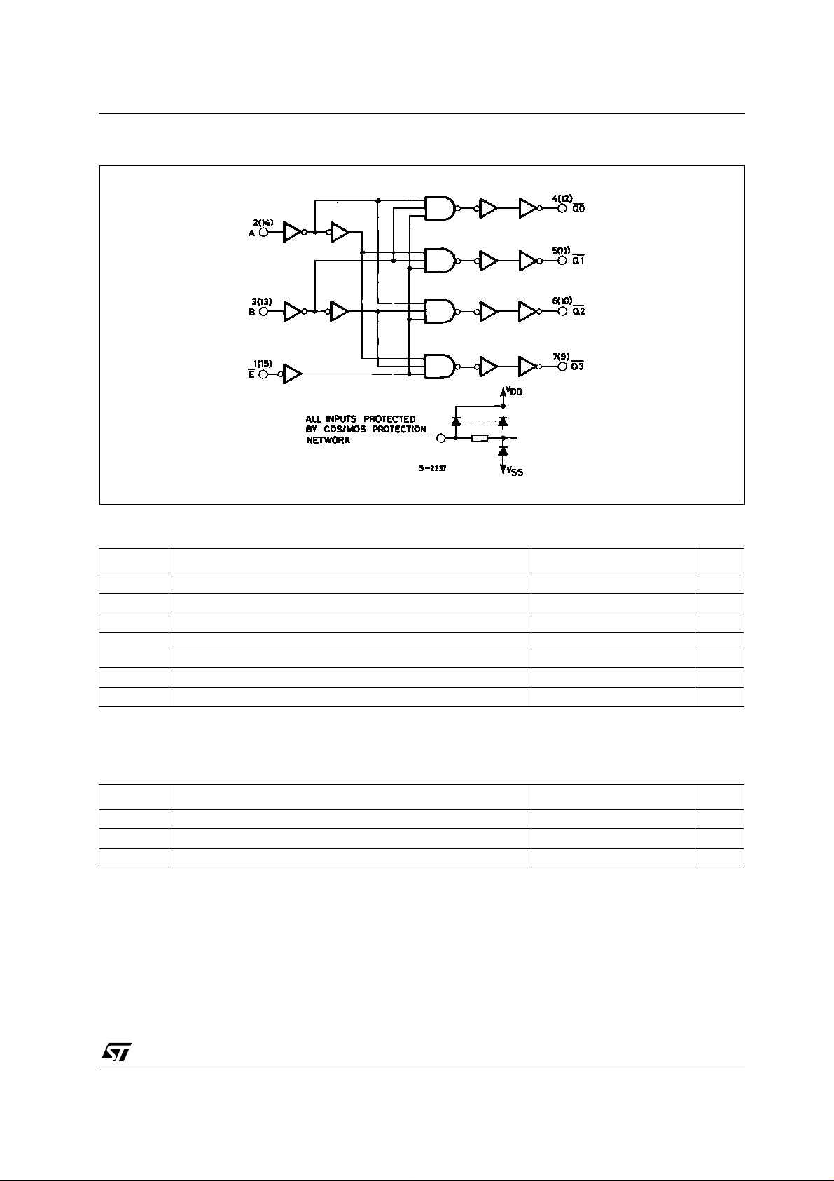
LOGIC DIAGRAM
HCF4556B
ABSOLUTE MAXIMUM RATINGS
Symbol Parameter Value Unit
V
V
P
Supply Voltage
DD
DC Input Voltage -0.5 to VDD + 0.5
I
I
DC Input Current
I
Power Dissipation per Package 200 mW
D
-0.5 to +22 V
± 10 mA
V
Power Dissipation per Output Transistor 100 mW
T
T
Absolute Maximum Ratings are those values beyond which damage to the device may occur. Functional operation under these conditions is
not implied.
All voltage values ar e referred t o V
Operating Temperature
op
Storage Temperature
stg
pin voltage.
SS
-55 to +125 °C
-65 to +150 °C
RECOMMENDED OPERATING CONDITIONS
Symbol Parameter Value Unit
V
V
T
Supply Voltage
DD
Input Voltage 0 to V
I
Operating Temperature
op
3 to 20 V
DD
-55 to 125 °C
V
3/9

HCF4556B
DC SPECIFICATIONS
Test Condition Value
T
Symbol Parameter
I
Quiescent Current 0/5 5 0.04 5 150 150
L
V
(V)
V
I
(V)
|I
|
O
O
(µA)
V
DD
(V)
= 25°C
A
Min. Typ. Max. Min. Max. Min. Max.
0/10 10 0.04 10 300 300
0/15 15 0.04 20 600 600
0/20 20 0.08 100 3000 3000
V
High Level Output
OH
Voltage
0/5 <1 5 4.95 4.95 4.95
0/15 <1 15 14.95 14.95 14.95
Low Level Output
V
OL
Voltage
5/0 <1 5 0.05 0.05 0.05
15/0 <1 15 0.05 0.05 0.05
High Level Input
V
IH
Voltage
0.5/4.5 <1 5 3.5 3.5 3.5
1.5/13.5 <1 15 11 11 11
V
IL
Low Level Input
Voltage
4.5/0.5 <1 5 1.5 1.5 1.5
13.5/1.5 <1 15 4 4 4
I
OH
Output Drive
Current
0/5 2.5 <1 5 -1.36 -3.2 -1.1 -1.1
0/5 4.6 <1 5 -0.44 -1 -0.36 -0.36
0/10 9.5 <1 10 -1.1 -2.6 -0.9 -0.9
0/15 13.5 <1 15 -3.0 -6.8 -2.4 -2.4
I
OL
Output Sink
Current
0/5 0.4 <1 5 0.44 1 0.36 0.36
0/15 1.5 <1 15 3.0 6.8 2.4 2.4
Input Leakage
I
I
Current
C
Input Capacitance
I
The Noi se Margin for both "1" and "0 " le vel is: 1V min. wi th VDD=5V, 2V min. with VDD=10V, 2.5V min. with VDD=15V
0/18 Any Input 18
Any Input 5 7.5 pF
±10
-5
-40 to 85°C -55 to 125°C
±0.1 ±1 ±1 µA
Unit
µA
V0/10 <1 10 9.95 9.95 9.95
V10/0 <1 10 0.05 0.05 0.05
V1/9 <1 10 7 7 7
V9/1 <1 10 3 3 3
mA
mA0/10 0.5 <1 10 1.1 2.6 0.9 0.9
DYNAMIC ELECTRICAL CHARACTERISTICS (T
Symbol Parameter
t
PLH tPHL
t
PLH tPHL
t
TLH tTHL
(*) Typical temperat ure coeffici ent for all VDD value is 0.3 %/°C.
Propagation Delay Time 5
Propagation Delay Time 5
Transition Time 5 100 200
4/9
(V)
V
DD
15 70 140
15 65 130
15 40 80
= 25°C, CL = 50pF, RL = 200KΩ, tr = tf = 20 ns)
amb
Test Condition Value (*) Unit
Min. Typ. Max.
220 440
A or B Input to any Output
ns10 95 190
200 400
Input to any Output
E
ns10 85 170
ns10 50 100

TYPICAL APPLICATIONS
1 OF 16 DECODER USING HCF4555B AND HCF4556B
TRUTH TABLE
INPUTS Q OUTPUTS
EDCBA0 123456789101112131415
000001000000000000000
000010100000000000000
000100010000000000000
000110001000000000000
001000000100000000000
001010000010000000000
001100000001000000000
001110000000100000000
010000000000010000000
010010000000001000000
010100000000000100000
010110000000000010000
011000000000000001000
011010000000000000100
011100000000000000010
011110000000000000001
1XXXX0000000000000000
HCF4556B
TEST CIRCUIT
CL = 50pF or equivalent (includes jig and p robe capacit ance)
= 200KΩ
R
L
= Z
R
of pulse generator (typically 50Ω)
T
OUT
5/9

HCF4556B
WAVEFORM 1 : PROPAGATION DELAY TIMES (INPUT TO Q3 OUTPUT) (f=1MHz; 50% duty cycle)
WAVEFORM 2 : PROPAGATION DELAY TIMES (E
INPUT TO Q3 OUTPUT) (f=1MHz; 50% duty cycle)
6/9

HCF4556B
Plastic DIP-16 (0.25) MECHANICAL DATA
mm. inch
DIM.
MIN. TYP MAX. MIN. TYP. MAX.
a1 0.51 0.020
B 0.77 1.65 0.030 0.065
b 0.5 0.020
b1 0.25 0.010
D 20 0.787
E 8.5 0.335
e 2.54 0.100
e3 17.78 0.700
F 7.1 0.280
I 5.1 0.201
L 3.3 0.130
Z 1.27 0.050
P001C
7/9

HCF4556B
SO-16 MECHANICAL DATA
DIM.
A 1.75 0.068
a1 0.1 0.2 0.003 0.007
a2 1.65 0.064
b 0.35 0.46 0.013 0.018
b1 0.19 0.25 0.007 0.010
C 0.5 0.019
c1 45° (typ.)
D 9.8 10 0.385 0.393
E 5.8 6.2 0.228 0.244
e 1.27 0.050
e3 8.89 0.350
F 3.8 4.0 0.149 0.157
G 4.6 5.3 0.181 0.208
L 0.5 1.27 0.019 0.050
M 0.62 0.024
S8° (max.)
MIN. TYP MAX. MIN. TYP. MAX.
mm. inch
8/9
PO13H

HCF4556B
Information furnished is bel ieved to be accurate and reliable. However, STMicroe lectronics assumes no responsibility for the
consequences of use of such information nor for any infringement of patents or other rights of third parties which may result from
its use. No li cense is granted by imp lication or otherwise under a ny patent or patent rig hts of STMicroelectronics. Specificat ions
mentioned in this publication ar e subject to change without notice. This publication supersedes and replaces all information
previously supplied. S TMicroelectronics products are not authorized for use as critica l components in life suppo rt devices or
systems without express written approval of STMicroelectronics.
Australi a - Brazil - Chin a - Finland - France - Germany - Hong Kon g - India - Italy - Japan - Malay si a - Malta - Morocco
© The ST logo is a registered trademark of STMicroelectronics
© 2001 STM icroelectronics - Pri n ted in Italy - A ll Ri g h ts Reserved
STMicr o el ectronics GROUP OF COMPANI ES
Singapo re - Spain - Sweden - Switzerland - Uni ted Kingdom
© http://www.st.com
9/9
 Loading...