

HCF4541B
PROGRAMMABLE TIMER
■ 16 STAGE BINARY COUNTER
■ LOW SYMMETR. OUTPUT RESISTANCE,
TYPICALLY 100Ω at V
■ OSCILLATOR FREQUENCY RANGE :
DD
= 15V
DC to 100KHz
■ AUTO OR MASTER RESET DISABLES
OSCILLATOR DURING RESET TO REDUCE
POWER DISSIPATION
■ OPERATES WITH VERY SLOW CLOCK
RISE AND FALL TIMES
■ BUILT-IN LOW-POWER RC OSCILLATOR
■ EXTERNAL CLOCK (applied to pin 3) CAN
BE USED INSTEAD OF OSCILLATOR
■ OPERATES A S 2
n
FREQUENCY DIVIDER
OR AS A SINGLE-TRANSITION TIMER
■ Q/Q SELECT PROVIDES OUTPUT LOGIC
LEVEL FLEXIBILITY
■ CAPABLE OF DRIVING SIX LOW POWER
TTL LOADS, THREE LOW POWER
SCHOTTKY LOADS, OR SIX HTL LOADS
OVER THE RATED TEMP. RANGE
■ 5V, 10V AND 15V PARAMETRIC RATINGS
■ 100% TESTED FOR QUIESCENT CURRENT
AT 20V
■ MEETS ALL REQUIREMENTS OF JEDEC
JESD13B " STANDARD SPECIFICATIONS
FOR DESCRIPTI ON OF B SERI ES CMOS
DEVICES"
DIP SOP
ORDER CODES
PACKAGE TUBE T & R
DIP HCF4541BEY
SOP HCF4541BM1 HCF4541M013TR
DESCRIPTION
The HCF4541B is a m onolithic integrated circuit
fabricated in Metal Oxide Semiconductor
technology available in DIP and SOP packages.
This device is composed of a 16-stages binary
counter, an oscillator controlled by 2 external
resistors and a capacitor, an o utput control logic
and an automatic power-on reset circuit. The
counter varies on positive-edge clock transition
and it can be cleared by the MASTER RESET
input. The output from this timer is the Q or Q
output from the 8th, 13th, or 16th counter stage.
The choice of the stage depends on the time
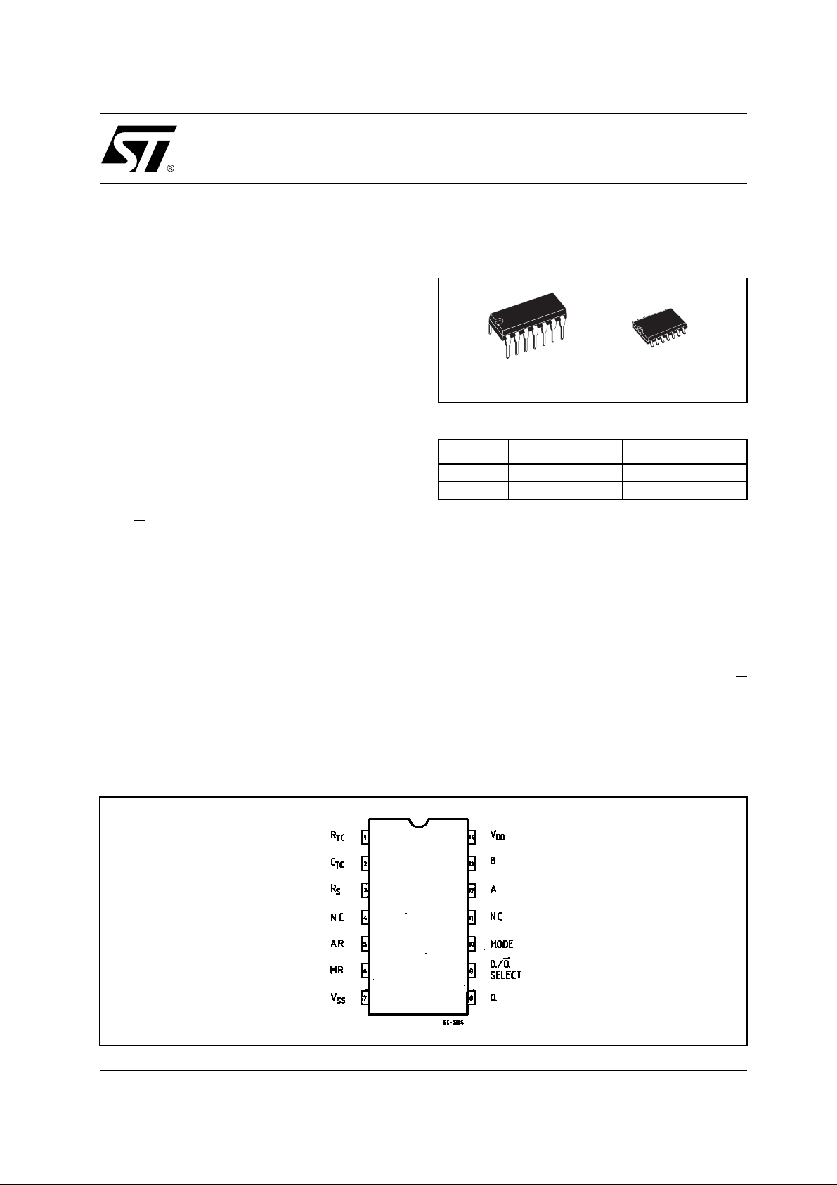
PIN CONNECTION
1/10September 2002
HCF4541B
select inputs A or B (see frequency selection
table). The output is available in one of the two
modes that can be selected via the M ODE input
pin 10 (see truth table). The output turns out as a
continuos square wave, with a frequenc y equal to
the oscillator frequency divided by 2
N
when this
MODE input is a logic "1". When it is a logic "0"
and after a MASTER RESET is started, and Q
output has been selected, the output goes up to a
high state after 2
N-1
counts. It remains in that
state till another M ASTER RE SET pulse is apply
or the mode input is a logic "1". The process starts
by setting the AUTO RESET input (pin 5) to logic
"0" and switching power on . If pin 5 is set to logic
"1", the AUTO RESET circuit is not enabled and
counting cannot start till a positive MASTER
RESET pulse is applied, returning to a low level.
The AUTO RESET consumes a remarkable
amount of po wer and should not be used if low
power operation is wanted. The frequenc y of the
oscillator depends on the RC network. It can be
calculated using the following formula :
f = 1 / 2.3 R
TC CTC
where f is between 1KHz and 100KHz and RS >
10 KΩ and ≈2 RTC
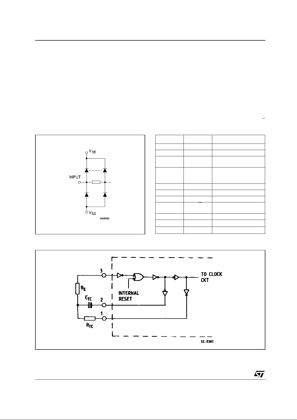
INPUT EQUIVALENT CIRCUIT PIN DESCRIPTION
PIN No SYMBOL NAME AND FUNCTION
12, 13 A, B Time Select Input
4, 11 NC Not Connected
, C
1, 2
3
5 AR Auto Reset Input
6 MR Master Reset Input
10 MODE Mode Select Input
9
8 Q Output
7
14
R
TC
R
S
Q/Q
SELECT
V
SS
V
DD
External Resistor, Capaci-
TC
tor Connection
External Resistor Con-
nection or External Clock
Input
Output Selector
Negative Supply Voltage
Positive Supply Voltage
RC OSCILLATOR CIRCUIT
2/10
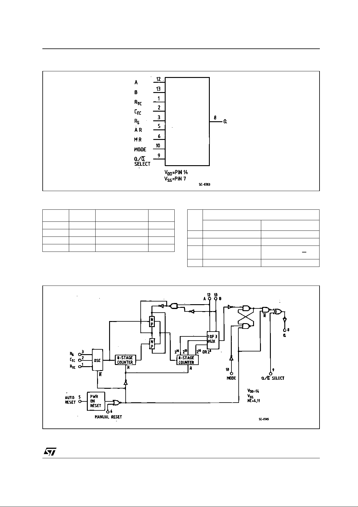
FUNCTIONAL DIAGRAM
FREQUENCY SELECTION TABLE TRUTH TABLE
HCF4541B
A B N. of Stages N
L L 13 8192
L H 10 1024
H L 8 256
H H 16 65536
LOGIC DIAGRAM
Count 2
N
PIN
5 Auto Reset On Auto Reset Disable
6 Master Reset Off Master Reset On
Output Initially Low
9
10 Single Transition Mode Recycle Mode
LH
After Reset (Q)
STATE
Output Initially High
After Reset (Q
)
3/10

HCF4541B
ABSOLUTE MAXIMUM RATINGS
Symbol Parameter Value Unit
V
V
P
T
T
Absolute Maximum Ratings are those values beyond which damage to the device may occur. Functional operation under these conditions is
not implied.
All voltage values are referred to V
RECOMMENDED OPERATING CONDITIONS
Symbol Parameter Value Unit
V
V
T
Supply Voltage
DD
DC Input Voltage -0.5 to VDD + 0.5
I
I
DC Input Current
I
Power Dissipation per Package 200 mW
D
-0.5 to +22 V
10 mA
±
Power Dissipation per Output Transistor 100 mW
Operating Temperature
op
Storage Temperature
stg
pin voltage.
SS
Supply Voltage
DD
Input Voltage 0 to V
I
Operating Temperature
op
-55 to +125 °C
-65 to +150 °C
3 to 20 V
DD
-55 to 125 °C
V
V
4/10

DC SPECIFICATIONS
Test Condition Value
T
Symbol Parameter
I
Quiescent Current 0/5 5 0.04 5 150 150
L
V
(V)
V
I
(V)
|I
|
O
O
(µA)
V
DD
(V)
= 25°C
A
Min. Typ. Max. Min. Max. Min. Max.
0/10 10 0.04 10 300 300
0/15 15 0.04 20 600 600
0/20 20 0.08 100 3000 3000
V
High Level Output
OH
Voltage
0/5 <1 5 4.95 4.95 4.95
0/15 <1 15 14.95 14.95 14.95
Low Level Output
V
OL
Voltage
5/0 <1 5 0.05 0.05 0.05
15/0 <1 15 0.05 0.05 0.05
High Level Input
V
IH
Voltage
0.5/4.5 <1 5 3.5 3.5 3.5
1.5/13.5 <1 15 11 11 11
V
IL
Low Level Input
Voltage
4.5/0.5 <1 5 1.5 1.5 1.5
13.5/1.5 <1 15 4 4 4
I
OH
Output Drive
Current
0/5 2.5 <1 5 -1.55 -3.1 -1.08 -1.08
0/5 4.6 <1 5 -5 -10 -3 -4.1
0/10 9.5 <1 10 -4 -8 -3.3 -3.3
0/15 13.5 <1 15 -10 -20 -8.4 -8.4
I
OL
Output Sink
Current
0/5 0.4 <1 5 1.55 3.1 1.08 1.08
0/15 1.5 <1 15 10 20 8.4 8.4
Input Leakage
I
I
Current
C
Input Capacitance
I
The Noi se Margin for bot h "1" and "0" leve l is: 1V min. with VDD=5V, 2V min. with VDD=10V, 2.5V min. with VDD=15V
0/18 Any Input 18
Any Input 5 7.5 pF
-5
10
±
-40 to 85°C -55 to 125°C
0.1
±
1
±
HCF4541B
Unit
A
µ
V0/10 <1 10 9.95 9.95 9.95
V10/0 <1 10 0.05 0.05 0.05
V1/9 <1 10 7 7 7
V9/1 <1 10 3 3 3
mA
mA0/10 0.5 <1 10 4 8 3.3 3.3
1
±
A
µ
5/10

HCF4541B
DYNAMIC ELECTRICAL CHARACTERISTICS (T
Symbol P arameter
8
(2
t
PHL tPLH
(2
t
PHL tPLH
t
t
t
(*) Typical temperature coefficien t f or all VDD value is 0.3 %/°C.
Propagation Delay Time
)
(CLOCK to Q)
16
Propagation Delay Time
)
(CLOCK to Q)
Transition Time 5 100 200
THL
Transition Time 5 180 360
TLH
Master Reset, Clock Pulse
Width
Maximum Clock Pulse
f
CL
Input Frequency
Maximum Clock Pulse
r, tf
Input Rise or Fall Time
(V)
V
DD
5 3.5 10.5
15 0.9 2.9
5618
15 2.5 7.5
15 40 80
15 65 130
5 900 300
15 225 85
51.5
15 6
5
15
= 25°C, CL = 50pF, RL = 200KΩ, tr = tf = 20 ns)
amb
Test Condition Value (*) U nit
Min. Typ. Max.
µ
µ
ns10 50 100
ns10 90 180
ns10 300 100
MHz10 4
Unlimited
µ
s10 1.25 3.8
s10 3.5 10
s10
DIGITAL TIMER APPLICATION
A positive MASTER RESET pulse clears the
counter and latch. The Output goes high and
keeps up till the number of pul ses, selected by A
and B , are counted. This circuit is retriggerable
and is as accurate as the input frequency. If a
more accurate circuit is desired, an external clock
can be used o n pin 3. A s et-up time equal to the
width of the one shot output is required
immediately following initial power up, during
which tim e the output will be hig h
6/10

TEST CIRCUIT
CL = 50pF or equivalent (includ es jig and probe capacitance)
= 200K
R
R
Ω
L
= Z
of pulse generator (typically 50Ω)
T
OUT
HCF4541B
7/10

HCF4541B
Plastic DIP-14 MECHANICAL DATA
mm. inch
DIM.
MIN. TYP MAX. MIN. TYP. MAX.
a1 0.51 0.020
B 1.39 1.65 0.055 0.065
b 0.5 0.020
b1 0.25 0.010
D 20 0.787
E 8.5 0.335
e 2.54 0.100
e3 15.24 0.600
F 7.1 0.280
I 5.1 0.201
L 3.3 0.130
Z 1.27 2.54 0.050 0.100
8/10
P001A

SO-14 MECHANICAL DATA
HCF4541B
DIM.
A 1.75 0.068
a1 0.1 0.2 0.003 0.007
a2 1.65 0.064
b 0.35 0.46 0.013 0.018
b1 0.19 0.25 0.007 0.010
C 0.5 0.019
c1 45˚ (typ.)
D 8.55 8.75 0. 336 0.344
E 5.8 6.2 0.228 0.244
e 1.27 0.050
e3 7.62 0.300
F 3.8 4.0 0. 149 0.157
G 4.6 5.3 0. 181 0.208
L 0.5 1.27 0.019 0.050
M 0.68 0.026
S ˚ (max.)
MIN. TYP MAX. MIN. TYP. MAX.
mm. inch
8
PO13G
9/10

HCF4541B
Information furnished is believed to be accurate and reliable. However, STMicroelectronics assumes no responsib ility f or the
consequences of use of such informatio n nor for any infringement of paten ts or o ther rig hts of t hird part ies which ma y result from
its use. No license is granted by implication or otherwise under any patent or patent rights of STMicroelectronics. Specifications
mentioned in this publication are subject to change without notice. This publication supersedes and replaces all information
previousl y suppl ied. STM icroel ectronics produc ts are not auth orized for use as c ritica l compone nts in l ife s upport dev ices or
systems without express written approval of STMicroelectronics.
Australia - Brazil - Canada - China - Finland - France - Germany - Hong Kong - India - Israel - Italy - Japan - Malaysia - Malta - Morocco
© The ST logo is a registered trademark of STMicroelectronics
© 2002 STMicroelectronics - Printed in Italy - All Rights Reserved
STMicroelectronics GROUP OF COMPANIES
Singapore - Spain - Sweden - Switzerland - United Kingdom - United States.
© http://www.st.com
10/10
 Loading...