

HCF4099B
8 BIT ADDRESSABLE LATCH
■ SERIAL DATA INPUT - ACTIVE PARALLEL
OUTPUT
■ STORAGE REGISTER CAPABILITY -
MASTER CLEAR
■ CAN FUNCTION AS DEMULTIPLEXER
■ QUIESCENT CURRENT SPECIFIED UP TO
20V
■ STANDARDIZED SYMMETRICAL OUTPUT
CHARACTERISTICS
■ INPUT LEAKAGE CURRENT
I
= 100nA (MAX) AT VDD = 18V TA = 25°C
I
■ 100% TESTED FOR QUIESCENT CURRENT
■ MEETS ALL REQUIREMENTS OF JEDEC
JESD13B "STANDARD SPECIFICATIONS
FOR DESCRIPTI ON OF B SERI ES CMOS
DEVICES"
DESCRIPTION
HCF4099B is a monolithic integrated circuit
fabricated in Metal Oxide Semiconductor
technology available in DIP and SOP packages.
HCF4099B, an 8-bit addressable latch, is a
serial-input, parallel output storage register that
can perform a variety of functions. Data is input to
a particular bit in the latch when that bit is
addressed (by means of input A0, A1, A2) and
when WRITE DISABLE is at a low level. When
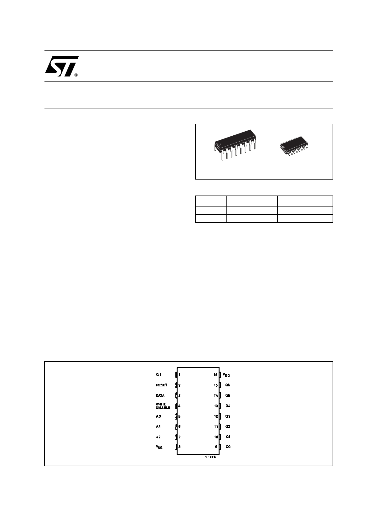
DIP SOP
ORDER CODES
PACKAGE TUBE T & R
DIP HCF4099BEY
SOP HCF4099BM1 HCF4099M013TR
WRITE DISABLE is high, data entry is inhibited;
however, all 8 ou tputs can be continuously re ad
independent of WRITE DISABLE and address
inputs. A mas ter RESET input is available, which
resets all bits to a logic "0" level when RESET and
WRITE DISABLE are at a high level. When
RESET is at a high level, and WRITE DISABLE is
at a low level, the latch acts as a 1-of-8
demultiplexer ; the bit that is addressed has an
active output which follows the data input, while all
unaddressed bits are held to a logic "0" level.
PIN CONNECTION
1/14October 2002

HCF4099B
IINPUT EQUIVALENT CIRCUIT PIN DESCRIPTION
PIN No SYMBOL NAME AND FUNCTION
5, 6, 7 A0 to A2 Address Inputs
9, 10, 11, 12,
13, 14, 15, 1
3 DATA Data Inputs
2 RESET Reset Input
4
8
16
FUNCTIONAL DIAGRAM
Q0 to Q7 Latch Outputs
WRITE
DISABLE
V
SS
V
DD
Write Disable Input
Negative Supply Voltage
Positive Supply Voltage
TRUTH TABLE
SELECT INPUTS
CBA
LLLQ0
LLHQ1
LHLQ2
LHHQ3
HLLQ4
HLHQ5
HHLQ6
HHHQ7
INPUTS OUTPUTS OF
WRITE DISABLE RESET
L L D Qi0 ADDRESSABLE LATCH
L H Qi0 Qi0 MEMORY
H L D L DEMULTIPLEXER
H H L L CLEAR ALL BITS TO "0"
D: The lev el at the data inp ut ; Qi0 The level before the indi cated steady st ate input cond i tions were es tablished , (i=0, 1,... 7)
2/14
ADDRESSED
LAT CH
EACH OTHER
OUTPUT
LATCH ADDRESSED
FUNCTION
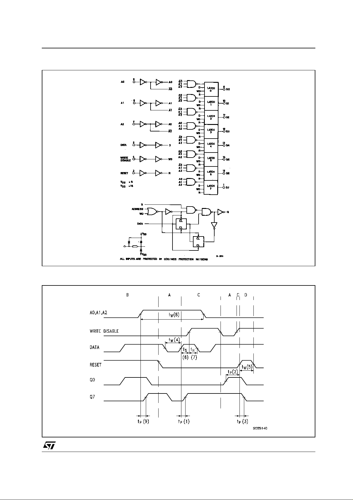
LOGIC DIAGRAM
HCF4099B
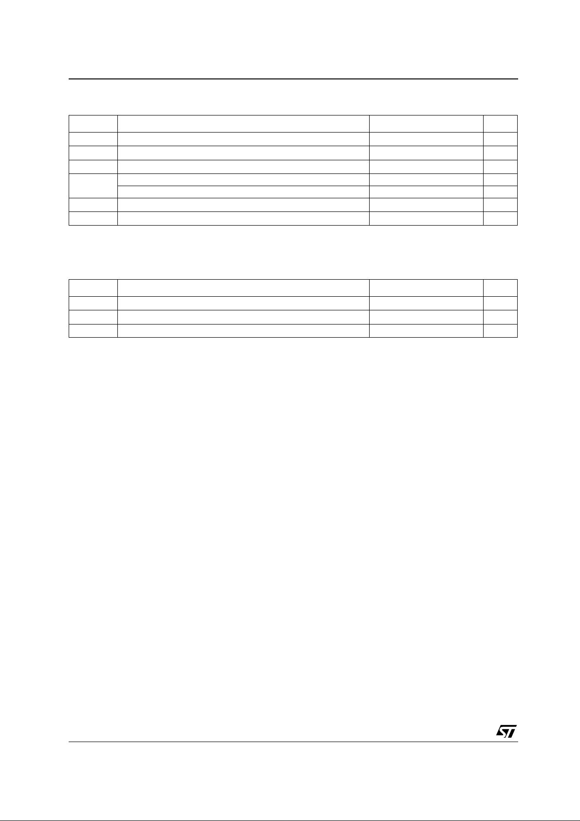
TIMING CHART
3/14
HCF4099B
ABSOLUTE MAXIMUM RATINGS
Symbol Parameter Value Unit
V
V
P
T
T
Absolute Maximum Ratings are those values beyond which damage to the device may occur. Functional operation under these conditions is
not implied.
All voltage values are referred to V
RECOMMENDED OPERATING CONDITIONS
Symbol Parameter Value Unit
V
V
T
Supply Voltage
DD
DC Input Voltage -0.5 to VDD + 0.5
I
I
DC Input Current
I
Power Dissipation per Package 200 mW
D
-0.5 to +22 V
10 mA
±
Power Dissipation per Output Transistor 100 mW
Operating Temperature
op
Storage Temperature
stg
pin voltage.
SS
Supply Voltage
DD
Input Voltage 0 to V
I
Operating Temperature
op
-55 to +125 °C
-65 to +150 °C
3 to 20 V
DD
-55 to 125 °C
V
V
4/14
DC SPECIFICATIONS
Test Conditions Value
T
Symbol Parameter
I
Quiescent Current 0/5 5 0.04 5 150 150
L
V
(V)
V
I
O
(V)
I
O
(µA)
V
DD
(V)
= 25°C
A
Min. Typ. Max. Min. Max. Min. Max.
0/10 10 0.04 10 300 300
0/15 15 0.04 20 600 600
0/20 20 0.08 100 3000 3000
V
High Level Output
OH
Voltage
0/5 <1 5 4.95 4.95 4.95
0/15 <1 15 14.95 14.95 14.95
Low Level Output
V
OL
Voltage
5/0 <1 5 0.05 0.05 0.05
15/0 <1 15 0.05 0.05 0.05
High Level Input
V
IH
Voltage
0.5/4.5 <1 5 3.5 3.5 3.5
1.5/18.5 <1 15 11 11 11
V
IL
Low Level Input
Voltage
0.5/4.5 <1 5 1.5 1.5 1.5
1.5/18.5 <1 15 4 4 4
I
OH
Output Drive
Current
0/5 2.5 5 -1.36 -3.2 -1.1 -1.1
0/5 4.6 5 -0.44 -1 -0.36 -0.36
0/10 9.5 10 -1.1 -2.6 -0.9 -0.9
0/15 13.5 15 -3.0 -6.8 -2.4 -2.4
I
OL
Output Sink
Current
0/5 0.4 5 0.44 1 0.36 0.36
0/15 1.5 15 3.0 6.8 2.4 2.4
Input Leakage
I
I
Current
C
Input Capacitance
I
The Noi se Margin fo r both "1" and "0" level is: 1V min. with VDD=5V, 2V min. with VDD=10V, 2.5V min. with VDD=15V
0/18 any input 18
any input 5 7.5 pF
-5
10
±
-40 to 85°C -55 to 125°C
0.1
±
1
±
HCF4099B
Unit
A
µ
V0/10 <1 10 9.95 9.95 9.95
V10/0 <1 10 0.05 0.05 0.05
V1/9 <1 10 7 7 7
V9/1 <1 10 3 3 3
mA
mA0/10 0.5 10 1.1 2.6 0.9 0.9
1
±
A
µ
5/14

HCF4099B
DYNAMIC ELECTRICAL CHARACTERISTICS (T
Symbol Parameter
t
PLH tPHL
t
PLH tPHL
t
PLH tPHL
t
t
THL tTLH
t
setup
t
(*) Typical temperature coefficient for all VDD value is 0.3 %/°C.
Propagation Delay Time
(Data to Output)
Propagation Delay Time
(Write Disable to Output)
Propagation Delay Time
(Address to Output)
Propagation Delay Time
PHL
(Reset to Output)
Transition Time
(any output)
Pulse WIdth (Data) 5
t
W
Pulse WIdth (Address) 5
t
W
Pulse WIdth (Reset) 5
t
W
Setup Time
(Data to Write Disable)
Hold Time
hold
(Data to Write Disable)
(V)
V
DD
5
15 50 100
5
15 60 120
5
15 75 150
5
15 65 130
5 100 200
15 40 80
15 80 40
15 125 65
15 50 25
5
15 35 20
5
15 50 25
= 25°C, CL = 50pF, RL = 200KΩ, tr = tf = 20 ns)
amb
Test Condition Value (*) Unit
See Timing Chart Min. Typ. Max.
200 400
(1)
ns10 75 150
200 400
(2)
ns10 80 160
225 450
(9)
ns10 100 200
175 350
(3)
ns10 80 160
ns10 50 100
200 100
(4)
ns10 100 50
400 200
(8)
ns10 200 100
150 75
(5)
ns10 75 40
100 50
(6)
ns10 50 25
150 75
(7)
ns10 75 40
6/14

TEST CIRCUIT
CL = 50pF or equivalent (in cludes jig and probe capac i t ance)
R
= 200K
Ω
L
R
= Z
of pulse generator (typically 50Ω)
T
OUT
WAVEFORM 1 : PROPAGATION DELAY TIME (f=1MHz; 50% duty cycle)
HCF4099B
7/14

HCF4099B
WAVEFORM 2 : PROPAGATION DELAY TIME (f=1MHz; 50% duty cycle)
WAVEFORM 3 : MINIMUM PULSE WIDTH, SETUP AND HOLD TIME (f=1MHz; 50% duty cycle)
8/14

WAVEFORM 4 : MINIMUM PULSE WIDTH (f=1M Hz ; 50% duty cycle)
HCF4099B
WAVEFORM 5 : SETUP AND HOLD TIME (f=1MHz; 50% duty cycle)
9/14

HCF4099B
WAVEFOR M 6 : I N P U T WA VEFORMS (f=1M Hz; 50% duty cycle)
TIPICAL APPLICATIONS
10/14

TIPICAL APPLICATIONS
HCF4099B
11/14

HCF4099B
Plastic DIP-16 (0.25) MECHANICAL DATA
mm. inch
DIM.
MIN. TYP MAX. MIN. TYP. MAX.
a1 0.51 0.020
B 0.77 1.65 0.030 0.065
b 0.5 0.020
b1 0.25 0.010
D 20 0.787
E 8.5 0.335
e 2.54 0.100
e3 17.78 0.700
F 7.1 0.280
I 5.1 0.201
L 3.3 0.130
Z 1.27 0.050
12/14
P001C

SO-16 MECHANICAL DATA
HCF4099B
DIM.
A 1.75 0.068
a1 0.1 0.2 0.003 0.007
a2 1.65 0.064
b 0.35 0.46 0.013 0.018
b1 0.19 0.25 0.007 0.010
C 0.5 0.019
c1 45˚ (typ.)
D 9.8 10 0.385 0.393
E 5.8 6.2 0. 228 0.244
e 1.27 0.050
e3 8.89 0.350
F 3.8 4.0 0.149 0.157
G 4.6 5.3 0.181 0.208
L 0.5 1.27 0.019 0.050
M 0.62 0.024
S ˚ (max.)
MIN. TYP MAX. MIN. TYP. MAX.
mm. inch
8
PO13H
13/14

HCF4099B
Information furnished is believed to be accurate and reliable. However, STMicroelectronics assumes no responsibi lity for the
consequences of use of such informatio n nor for any infringement of paten ts or o ther rig hts of t hird part ies which ma y result from
its use. No license is granted by implication or otherwise under any patent or patent rights of STMicroelectronics. Specifications
mentioned in this publication are subject to change without notice. This publication supersedes and replaces all information
previousl y suppl ied. STM icroel ectronics produc ts are not auth orized for use as c ritica l compone nts in l ife s upport dev ices or
systems without express written approval of STMicroelectronics.
Australia - Brazil - Canada - China - Finland - France - Germany - Hong Kong - India - Israel - Italy - Japan - Malaysia - Malta - Morocco
© The ST logo is a registered trademark of STMicroelectronics
© 2002 STMicroelectronics - Printed in Italy - All Rights Reserved
STMicroelectronics GROUP OF COMPANIES
Singapore - Spain - Sweden - Switzerland - United Kingdom - United States.
© http://www.st.com
14/14
 Loading...