

查询HCF4098 供应商
HCF4098B
DUAL MONOSTABLE MULTIVIBRATOR
■ RETRIGGERABLE/RESETTABLE
CAPABILITY
■ TRIGGER AND RESET PROPAGATION
DELAYS INDEPENDENT OF R
■ TRIGGERING FROM LEADING OR
, C
X
X
TRAILING EDGE
■ Q AND Q BUFFERED OUTPUT AVAILABLE
■ SEPARATE RESETS
■ WIDE RANGE OF OUTPUT PULSE WIDTHS
■
QUIESCENT CURRENT SPECIFIED UP TO
20V
■ 5V, 10V AND 15V PARAMETRIC RATINGS
■ INPUT LEAKAGE CURRENT
= 100nA (MAX) AT VDD = 18V TA = 25°C
I
I
■ 100% TESTED FOR QUIESCENT CURRENT
■ MEETS ALL REQUIREMENTS OF JEDEC
JESD13B " STANDARD SPECIFICAT IONS
FOR DESCRIPTI ON OF B SERI ES CMOS
DEVICES"
DESCRIPTION
The HCF4098B is a m onolithic integrated circuit
fabricated in Metal Oxide Semiconductor
technology available in DIP and SOP packages.
The HCF4098B dual precision monostable
multivibrator provides stable retriggerable/
resettable one-shot operation for any fixed voltage
timing application. An external resistor (R
an external capacitor (C
the circuit. Adjustment of R
) control the timing for
X
and CX provides a
X
) and
X
DIP SOP
ORDER CODES
PACKAGE TUBE T & R
DIP HCF4098BEY
SOP HCF4098BM1 HCF4098M013TR
wide range of output pulse widths from t he Q and
Q
terminals. The time delay from trigger input to
output transition (trigger propagation delay) and
the time delay from reset input to output transition
(reset propagation delay) and the time delay from
reset input to o utput transition (reset propagation
delay) are independent of R
and CX. Leading
X
edge triggering (+TR) and trailing edge triggering
(-TR) inputs are provided for triggering from either
edge of an input pulse. An unused +TR input
shoul d b e t i ed t o V
be tied to V
DD
. An unused -TR input should
SS
. A RESET (on low leve l) is provi ded
for immediate termination of the output pulse or to
prevent output pulses w hen power is turned on.
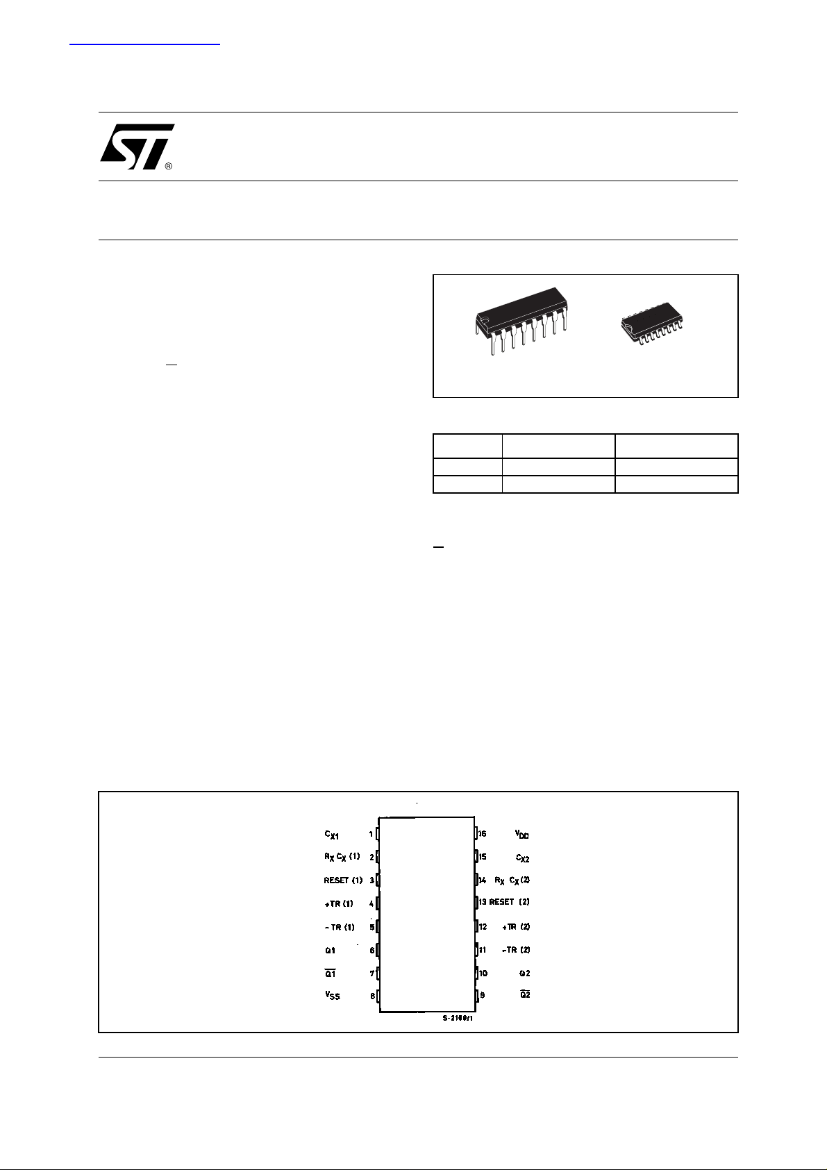
PIN CONNECTION
1/10September 2001
HCF4098B
An unused RESET input should be tied to VDD .
However, if an ent ire section of the HCF4098 B is
not used, its reset should be tied to V
(see table
SS
1). In normal operation the circuit triggers (extends
the output pulse one period) on the appl ication of
each new trigger pulse. For operation in the
non-retiggerable mode, Q
is connected to -TR
when leading edge triggering (+TR) is used or Q is
connected to +TR when trailing edge triggering
(-TR) is used. The time period (T) for this
multivibrator can be calculated by : T = 1/2 R
for CX > 0.01µF. The min. value of external
resistance, R
, is 5KΩ. The max. values of
X
external capacitan ce, C
pulse width has variations of ±2.5% typically, over
the temperature range of -55 °C to 125 °C for
=1000pF and RX = 100KΩ . For power sup ply
C
X
variation of ±5% typically , for V
and ±1% typically for V
and R
= 5KΩ .
X
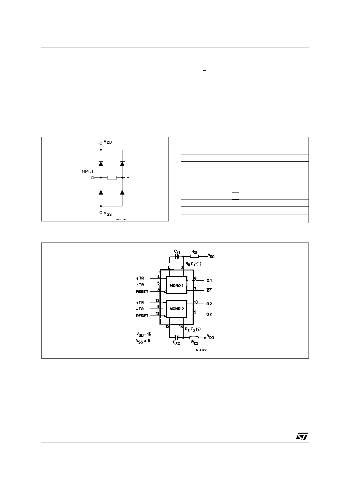
IINPUT EQUIVALENT CIRCUIT PIN DESCRIPTION
PIN No SYMBOL NAME AND FUNCTION
4, 12 +TR Leading Trigger Inputs
5, 11 -TR Trailing Trigger Inputs
3, 13 RE SET Reset Inputs
1, CX2
1, 15
2, 14
6, 7 Q1, Q1
10, 9 Q2, Q2
8
16
C
X
R
XCX
R
XCX
V
SS
V
DD
, is 100 µF. T he output
X
= 10V and 15V
DD
= 5V at CX = 1000pF
DD
External Capacitors
1
External resistors to Vdd
2
Ouputs Mono 1
Outputs Mono 2
Negative Supply Voltage
Positive Supply Voltage
X CX
FUNCTIONAL DIAGRAM
2/10
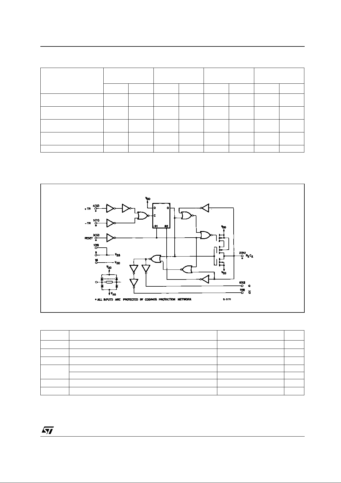
TABLE 1 : Func ti onal Termi nal Co nnections
HCF4098B
Input Pulse to
Term. N°
Other Connections
FUNCTION
to Term. N° VSS to Term. N°
V
DD
Mono (1) Mono (2) Mono (1) Mono (2) Mono (1) Mono (2) Mono (1) Mono (2)
Leading Edge Trigger/
Retriggerable
Leading Edge Trigger/Non
Retriggerable
Trailing Edge Trigger/
Retriggerable
Trailing Edge Trigger/Non
Retriggerable
3, 5 11, 13 4 12
3 13 4 12 5, 7 11, 9
3 13 4 12 5 11
3 13 5 11 4, 6 12, 10
Unused Section 5 11 3, 4 12, 13
A Retriggerable one-shot multivibrator has an output pulse width which is extended on full time period (T) after application of the last trigger
pulse .
A Non-Retriggerable one-s hot multiv ibrator has a time period (T ) referenced from th e application of the fir s t ri gger pulse .
LOGIC DIAGRAM
ABSOLUTE MAXIMUM RATINGS
Symbol Parameter Value Unit
V
V
P
T
T
Absolute Maximum Ratings are those values beyond which damage to the device may occur. Functional operation under these conditions is
not implied.
All voltage values are referred to V
Supply Voltage
DD
DC Input Voltage -0.5 to VDD + 0.5
I
I
DC Input Current
I
Power Dissipation per Package 200 mW
D
-0.5 to +22 V
± 10 mA
Power Dissipation per Output Transistor 100 mW
Operating Temperature
op
Storage Temperature
stg
pin voltage.
SS
-55 to +125 °C
-65 to +150 °C
V
3/10

HCF4098B
RECOMMENDED OPERATING CONDITIONS
Symbol Parameter Value Unit
V
V
T
DC SPECIFICATIONS
Symbol Parameter
I
L
V
OH
V
OL
V
IH
V
IL
I
OH
I
OL
I
I
C
I
The Noi se Margin fo r both "1" and "0" level is: 1V min. with VDD=5V, 2V min. with VDD=10V, 2.5V min. with VDD=15V
Supply Voltage
DD
Input Voltage 0 to V
I
Operating Temperature
op
3 to 20 V
DD
-55 to 125 °C
Test Condition Value
V
(V)
= 25°C
V
I
(V)
|I
|
O
O
(µA)
V
DD
(V)
A
Min. Typ. Max. Min. Max. Min. Max.
-40 to 85°C -55 to 125°C
T
Quiescent Current 0/5 5 0.02 1 30 30
0/10 10 0.02 2 60 60
0/15 15 0.02 4 120 120
0/20 20 0.04 20 600 600
High Level Output
0/5 <1 5 4.95 4.95 4.95
Voltage
0/15 <1 15 14.95 14.95 14.95
Low Level Output
5/0 <1 5 0.05 0.05 0.05
Voltage
15/0 <1 15 0.05 0.05 0.05
High Level Input
0.5/4.5 <1 5 3.5 3.5 3.5
Voltage
1.5/13.5 <1 15 11 11 11
Low Level Input
4.5/0.5 <1 5 1.5 1.5 1.5
Voltage
13.5/1.5 <1 15 4 4 4
Output Drive
Current
0/5 2.5 <1 5 -1.6 -3.2 -1.3 -1.3
0/5 4.6 <1 5 -0.51 -1 -0.42 -0.42
0/10 9.5 <1 10 -1.3 -2.6 -1.1 -1.1
0/15 13.5 <1 15 -3.4 -6.8 -2.8 -2.8
Output Sink
0/5 0.4 <1 5 -0.51 1 -0.42 -0.42
Current
0/15 1.5 <1 15 -3.4 6.8 -2.8 -2.8
Input Leakage
Current
Input Capacitance
0/18 Any Input 18
Any Input 5 7.5 pF
±10
-5
±0.1 ±1 ±1 µA
V
Unit
µA
V0/10 <1 10 9.95 9.95 9.95
V10/0 <1 10 0.05 0.05 0.05
V1/9 <1 10 7 7 7
V9/1 <1 10 3 3 3
mA
mA0/10 0.5 <1 10 -1.3 2.6 -1.1 -1.1
4/10

HCF4098B
DYNAMIC ELECTRICAL CHARACTERISTICS (T
Symbol Parameter
t
PLH tPHL
t
WH tWL
t
t
t
PLH tPHL
t
t
r, tf
Propagation Delay Time
+TR or -TR to Q or Q
Trigger Pulse Width
Transition Time
TLH
Transition Time
THL
Propagation Delay Time
(Reset)
Pulse Width (reset)
WR
(TR) Rise or Fall Time (trigger)
Pulse Width Match Between
Circuits in Same Package
(*) Typical temperature coefficient for a ll VDD value is 0.3 %/°C.
(KΩ)C
R
X
5 to 10000 >15
5 to 10000 >
5 to 10000 >
5 to 10000 15 to 10000
5 to 10000
5 to 10000
5 to 10000 >
100
10 10000
= 25°C, CL = 50pF, RL = 200KΩ, tr = tf = 20 ns)
amb
Test Condition Value (*) Unit
(pF) VDD (V)
X
Min. Typ. Max.
5 250 500
15 100 200
514070
15
15 40 20
5 100 200
15
15 40 80
5 100 200
10 50 100
15 40 80
0.01µF
to 0.1µF
0.1µF
to 1µF
5 150 300
10 75 150
15 65 130
5 250 500
10 150 300
15 80 160
5 225 450
15
15 75 150
5 200 100
15
10 80 40
15 60 30
5 1200 600
1000
10 600 300
15 500 250
5 50 250
0.1µF
15 20 10
5 to 15 100 µs
5510
15 7.5 15
ns10 125 250
ns10 60 30
ns10 50 100
ns
ns10 125 250
ns
µs10 30 15
%10 7.5 15
5/10

HCF4098B
TEST CIRCUIT
CL = 50pF or equivalent (in cludes jig and probe capaci tance)
= 200KΩ
R
L
R
= Z
of pulse generator (typically 50Ω)
T
OUT
6/10

HCF4098B
7/10

HCF4098B
Plastic DIP-16 (0.25) MECHANICAL DATA
mm. inch
DIM.
MIN. TYP MAX. MIN. TYP. M AX.
a1 0.51 0.020
B 0.77 1.65 0.030 0.065
b 0.5 0.020
b1 0.25 0.010
D 20 0.787
E 8.5 0.335
e 2.54 0.100
e3 17.78 0.700
F 7.1 0.280
I 5.1 0.201
L 3.3 0.130
Z 1.27 0.050
8/10
P001C

SO-16 MECHANICAL DATA
HCF4098B
DIM.
A 1.75 0.068
a1 0.1 0.2 0.003 0.007
a2 1.65 0.064
b 0.35 0.46 0.013 0.018
b1 0.19 0.25 0.007 0.010
C 0.5 0.019
c1 45° (typ.)
D 9.8 10 0.385 0.393
E 5.8 6.2 0.228 0.244
e 1.27 0.050
e3 8.89 0.350
F 3.8 4.0 0.149 0.157
G 4.6 5.3 0.181 0.208
L 0.5 1.27 0.019 0.050
M 0.62 0.024
S8° (max.)
MIN. TYP MAX. M IN. TYP. MAX.
mm. inch
PO13H
9/10

HCF4098B
Information furnished is bel ieved to be accurate and reliable. However, STMicroe lectronics assumes no responsibility for the
consequences of use of such information nor for any infringement of patents or other rights of third parties which may result from
its use. No li cense is granted by i mp lication or otherwise under a ny patent or patent rig hts of STMicroelectronics. S pec ificat ions
mentioned in this publication ar e subject to change without notice. This publication supersedes and replaces all information
previously supplied. S TMicroelectronics products are not authorized for use as critica l components in life suppo rt devices or
systems without express written approval of STMicroelectronics.
Australi a - Brazil - Chi na - Finlan d - F rance - Germ any - Hong Kon g - India - Italy - Japan - Mal a ysia - Malta - Morocco
© The ST logo is a registered trademark of STMicroelectronics
© 2001 STM icroelectronics - P rinted in Italy - All Rights Reserv ed
STMicr o el ectronics GROUP OF COMPA NI E S
Singapo re - Spain - Sweden - Swit zerland - Un i ted Kingdom
© http://www.st.com
10/10
 Loading...