

8 STAGE SHIFT AND STORE BUS REGISTER
■ 3-STATE PARALLELOUTPUTS FOR
CONNECTION TO COMM ON BUS
■ SEPARATE SERIAL OUTPUTS
SYNCHRONOUS TO BOTH POSITIVE AND
NEGATIVE CLOCK EDGES FOR
CASCADING
■ MEDIUM SPEED OPERATION 5MHz at 10V
■ QUIESCENT CURRENT SPECIFIED UP TO
20V
■ STANDARDIZED SYMMETRICAL OUTPUT
CHARACTERISTICS
■ 5V,10V AND 15V PARAMETRIC RATINGS
■ INPUT LEAKAGE CURRE NT
I
= 100nA (MAX) AT VDD=18VTA= 25°C
I
■ 100% TESTED FOR QUIESCENT CURRENT
DESCRIPTION
The HCF4094B is a monolithic integrated circuit
fabricated in Metal Oxide Semiconductor
technology available in DIP and SOP packages.
The HCF4094B is an 8 stages serial shift register
having a st orage latch associated with each stage
for strobing data from the serial input to parallel
buffered 3-state outputs. The parallel outputs may
be connected directly to common bus lines. Data
is shifted on positive clock transition. The data in
each shift register stage is transferred to the
HCF4094B
WITH 3-STATE OUTPUTS
DIP SOP
ORDER CODES
PACKAGE TUBE T & R
DIP HCF4094BEY
SOP HCF4094BM1 HCF4094M013TR
storage register when the STROBE input is high.
Data in the storage register appears at the outputs
whenever the OUTPUT-E N ABLE signal is high.
Two serial output s are available for casc ading a
number of HCF4094B devices. Data is available
at the Q
edges to allow for high speed operation in
cascaded system in which the clock rise time is
fast. The sam e serial information, available at the
Q’
S
provides a means for cascading HCF4094B
devices when the clock rise time is slow.
serial output terminal on p os itive clock
S
terminal on the next negative clock edge,
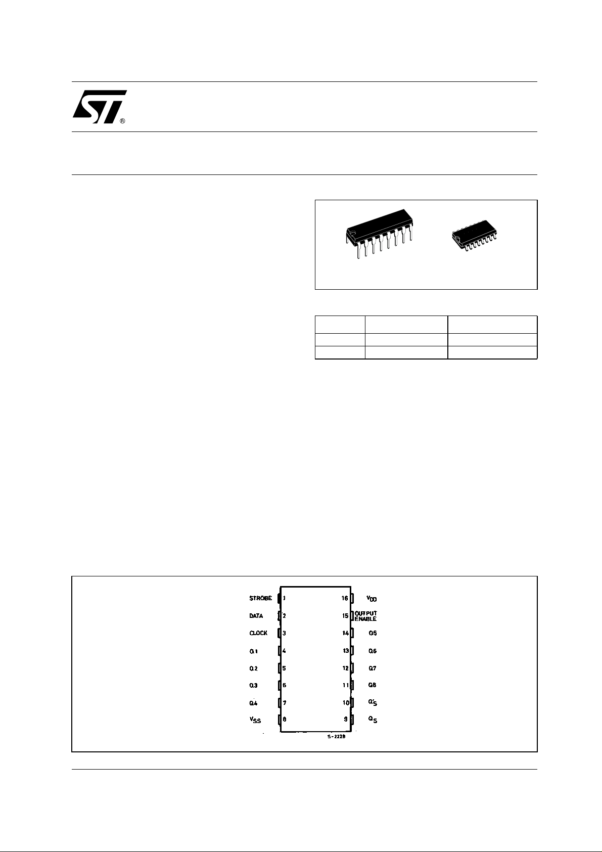
PIN CONNECTION
1/13March 2004
HCF4094B
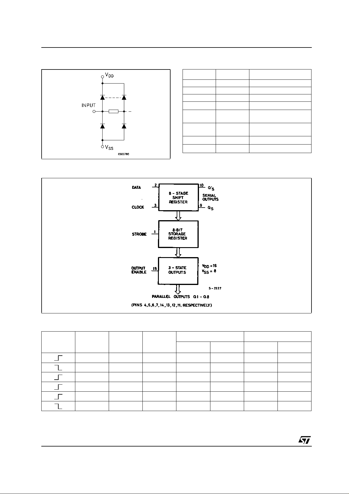
IINPUT EQUIVALENT CIRCUIT PIN DESCRIP TION
PIN N° SYMBOL NAME AND FUNCTION
2 DATA Data Input
1 STROBE Strobe Input
3 CLOCK Clock Input
9, 10
4, 5, 6, 7, 14,
13, 12, 11
15
8
16
FUNCTIONAL DIAGRAM
Q
S
Q1 to Q8
OUTPUT
ENABLE
V
V
,Q’
SS
DD
Serial Outputs
S
Parallel Outputs
Output Enable Input
Negative Supply Voltage
Positive Supply Voltage
TRUTH TABLE
CLOCK
OUTPUTS
ENABLE
STROBE DATA
L X X OC OC Q7 No Change
L X X OC OC No Change Q7
H L X No Change No Change Q7 No Change
HHLL
HHHH
H H H No Change No Change No Change Q7
X : Don’tCare
OC : Open Circuit
* At the positive clock edge information on the 7th shift register stage is transferred to the 8th register stage and the QSoutput.
2/13
PARALLEL OUTPUTS SERIAL OUTPUTS
Q
1
Q
n
-1
Q
n
-1
Q
n
Q*
S
Q7 No Change
Q7 No Change
Q’
S
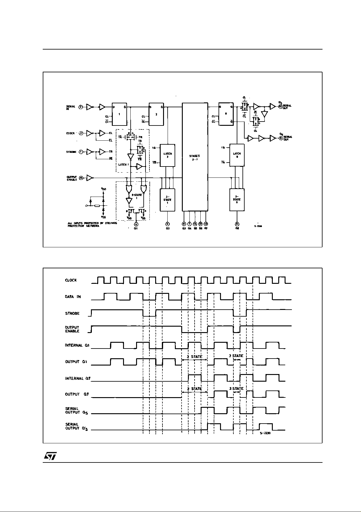
LOGIC DIAGRAM
HCF4094B
TIMING CHART
3/13
HCF4094B
ABSOLUTE MAXIMUM RATINGS
Symbol Parameter Value Unit
V
V
P
T
T
stg
Absolute Maximum Ratings are those values beyond which damage to the device may occur. Functional operation under these conditions is
not implied.
All voltagevalues arereferredto V
(*) 500mW at65
RECOMMENDED OPERATING CONDITIONS
Symbol Parameter Value Unit
V
V
T
Supply Voltage
DD
DC Input Voltage -0.5 to VDD+0.5
I
DC Input Current
I
I
Power Dissipation per Package 500 (*) mW
D
-0.5 to +22 V
± 10 mA
Power Dissipation per Output Transistor 100 mW
Operating Temperature
op
Storage Temperature
pin voltage.
°C; derate to 300mW by 10mW/°Cfrom65°Cto85°C
Supply Voltage
DD
Input Voltage 0 to V
I
Operating Temperature
op
SS
-55 to +125 °C
-65 to +150 °C
3to20 V
DD
-55 to 125 °C
V
V
4/13

DC SPECIFICATIONS
Test Condition Value
T
Symbol Parameter
I
Quiescent Current 0/5 5 0.04 5 150 150
L
V
(V)
V
I
(V)
|I
|
O
O
(µA)
V
DD
(V)
= 25°C
A
Min. Typ. Max. Min. Max. Min. Max.
0/10 10 0.04 10 300 300
0/15 15 0.04 20 600 600
0/20 20 0.08 100 3000 3000
V
High Level Output
OH
Voltage
0/5 <1 5 4.95 4.95 4.95
0/15 <1 15 14.95 14.95 14.95
V
Low Level Output
OL
Voltage
5/0 <1 5 0.05 0.05 0.05
15/0 <1 15 0.05 0.05 0.05
V
High Level Input
IH
Voltage
0.5/4.5 <1 5 3.5 3.5 3.5
1.5/13.5 <1 15 11 11 11
V
Low Level Input
IL
Voltage
4.5/0.5 <1 5 1.5 1.5 1.5
13.5/1.5 <1 15 4 4 4
I
OH
Output Drive
Current
0/5 2.5 5 -1.36 -3.2 -1.1 -1.1
0/5 4.6 5 -0.44 -1 -0.36 -0.36
0/10 9.5 10 -1.1 -2.6 -0.9 -0.9
0/15 13.5 15 -3.0 -6.8 -2.4 -2.4
I
OL
Output Sink
Current
0/5 0.4 5 0.44 1 0.36 0.36
0/15 1.5 15 3.0 6.8 2.4 2.4
I
Input Leakage
I
Current
I
OH,IOL
The Noise Margin forboth "1"and "0" level is:1V min. with VDD=5V, 2V min. with VDD=10V, 2.5V min. with VDD=15V
3-State Output
Leakage Current
Input Capacitance
C
I
0/18 Any Input 18
0/18 0/18 18
Any Input 5 7.5 pF
±10
±10
-5
-4
-40 to 85°C -55 to 125°C
± 0.1 ± 1 ± 1 µA
± 0.4 ± 12 ± 12 µA
HCF4094B
Unit
µA
V0/10 <1 10 9.95 9.95 9.95
V10/0 <1 10 0.05 0.05 0.05
V1/9 <1 10 7 7 7
V9/1 <1 10 3 3 3
mA
mA0/10 0.5 10 1.1 2.6 0.9 0.9
5/13

HCF4094B
DYNAMIC ELECTRICAL CH ARACTERISTICS (T
Symbol Parameter
t
PLHtPHL
t
PLHtPHL
t
PLHtPHL
t
PLHtPHL
t
PZL,tPZH
Propagation Delay Time
(Clock to serial Output Q
)
S
Propagation Delay Time
(Clock to serial Output Q’
)
S
Propagation Delay Time
(Clock to Parallel Output)
Propagation Delay Time
(Strobe to Parallel Output)
Propagation Delay Time
Output Enable to Parallel Out:
Output High to High Impedance
t
PHZtPLZ
Propagation Delay Time
Output Enable to Parallel Out:
Output Low to High Impedance
t
Strobe Pulse Width 5 200 100
W
t
Clock Pulse Width 5 200 100
W
t
setup
t
t
TLHtTHL
f
(*) Typical temperature coefficient for all VDDvalue is 0.3%/°C.
Data Setup Time 5 125 60
Minimum Hold Time 5 0 0 0
hold
Transition Time 5 100 200
t
Clock input Rise or Fall Time 5 15
r,tf
Maximum Clock Input
max
Frequency
(V)
V
DD
5 300 600
15 95 190
5 230 460
15 75 150
5 420 840
15 135 270
5 290 580
15 100 200
5 140 280
15 55 110
5 225 450
10 95 190
15 70 140
15 70 35
15 83 40
15 35 20
15 0 0 0
15 40 80
15 5
51.252.5
15 3 6
=25°C,CL= 50pF, RL= 200KΩ,tr=tf=20ns)
amb
Test Condition Value (*) Unit
Min. Typ. Max.
ns10 125 250
ns10 110 220
ns10 195 390
ns10 145 290
ns10 75 150
ns
ns10 80 40
ns10 100 50
ns10 55 30
ns10 0 0 0
ns10 50 100
µs10 5
MHz10 2.5 5
6/13

TYPICAL APPLICATION (REMOTE CONTROL HOLDING REGISTE R)
HCF4094B
TEST CIRCUIT
TEST SWITCH
t
PLH,tPHL
t
PZL,tPLZ
t
PZH,tPHZ
CL= 50pF or equivalent (includes jig and probe capacitance)
R
=200KΩ
L
R
T=ZOUT
of pulse generator (typically 50Ω)
Open
V
CC
GND
7/13

HCF4094B
WAVEFORM 1: PROPAGATION DELAY TIMES , PULSE WIDTH (CLOCK), SE TUP AND HOLD TIME
(DATA IN TO CL OCK) (f=1MHz; 50 % duty cycle)
WAVEFORM 2: PROPAGATION D ELAY TIME, PULSE WIDTH (STROBE), SETUP AND HOLD TIME
(STROBE TO CLOCK) (f=1MHz; 50% duty cycle)
8/13

WAVEFORM 3: OUTPUT ENABLE AND DISABLE TIME (f=1MHz; 50% duty cycle)
HCF4094B
9/13

HCF4094B
Plastic DIP-16 (0.25) MECHANICAL DATA
mm. inch
DIM.
MIN. TYP MAX. MIN. TYP. MAX.
a1 0.51 0.020
B 0.77 1.65 0.030 0.065
b 0.5 0.020
b1 0.25 0.010
D 20 0.787
E 8.5 0.335
e 2.54 0.100
e3 17.78 0.700
F 7.1 0.280
I 5.1 0.201
L 3.3 0.130
Z 1.27 0.050
10/13
P001C

SO-16 MECHANICAL DATA
HCF4094B
DIM.
A 1.75 0.068
a1 0.1 0.2 0.004 0.008
a2 1.65 0.064
b 0.35 0.46 0.013 0.018
b1 0.19 0.25 0.007 0.010
C 0.5 0.019
c1 45˚ (typ.)
D 9.8 10 0.385 0.393
E 5.8 6.2 0.228 0.244
e 1.27 0.050
e3 8.89 0.350
F 3.8 4.0 0.149 0.157
G 4.6 5.3 0.181 0.208
L 0.5 1.27 0.019 0.050
M 0.62 0.024
S8 ˚ (max.)
MIN. TYP MAX. MIN. TYP. MAX.
mm. inch
PO13H
11/13

HCF4094B
Tape & Reel SO-16 MECHANICAL DATA
mm. inch
DIM.
MIN. TYP MAX. MIN. TYP. MAX.
A 330 12.992
C 12.8 13.2 0.504 0.519
D 20.2 0.795
N 60 2.362
T 22.4 0.882
Ao 6.45 6.65 0.254 0.262
Bo 10.3 10.5 0.406 0.414
Ko 2.1 2.3 0.082 0.090
Po 3.9 4.1 0.153 0.161
P 7.9 8.1 0.311 0.319
12/13

HCF4094B
Information furnished is believed to be accurate and reliable. However, STMicroelectronics assumes no responsibility for the
consequences of use of such inform ation nor fo r an y infring ement of p atents or o ther rights of third p arties which may r esult f rom
its use. No license is granted by implication or otherwise under any patent or patent rights of STMicroelectronics. Specifications
mentioned in this publication are subject to change without notice. This publication supersedes and replaces all information
previously supplied. STMicroelectronics products are not authorized for use as critical components in life support devices or
systems without express written approval of STMicroelectronics.
Australia - Belgium - Brazil - Canada - China - Czech Republic - Finland - France - Germany - Hong Kong - India - Israel - Italy - Japan -
Malaysia - Malta - Morocco - Singapore - Spain - Sweden - Switzerland - United Kingdom - United States.
The ST logo is a registered trademark of STMicroelectronics
All other names are the property of their respective owners
© 2004 STMicroelectronics - All Rights Reserved
STMicroelectronics GROUP OF COMPANIES
http://www.st.com
13/13
 Loading...