

Page 1
HCF4093B
QUAD 2 INPUT NAND SCHMITT TRIGGER
■ SCHMITT TRIGGER ACTION ON EACH
INPUT WITH NO EXT ER NAL COMPONENTS
■ HYSTERESIS VOLTAGE TYPICALLY 0.9V at
V
= 5V AND 2.3V at VDD = 10V
DD
■ NOISE IMMUNITY GREATER THAN 50%OF
V
(Typ.)
DD
■ NO LIMIT ON INPUT RISE AND FALL TIMES
■ QUIESCENT CURRENT SPECIFIED UP TO
20V
■ STANDARDIZED SYMMETRICAL OUTPUT
CHARACTERISTICS
■ 5V, 10V AND 15V PARAMETRIC RATINGS
■ INPUT LEAKAGE CURRENT
I
= 100nA (MAX) AT VDD = 18V TA = 25°C
I
■ 100% TESTED FOR QUIESCENT CURRENT
■ MEETS ALL REQUIREMENTS OF JEDEC
JESD13B " STANDARD SPECIF ICATIONS
FOR DESCRIPTI ON OF B SERI ES CMOS
DEVICES"
DESCRIPTION
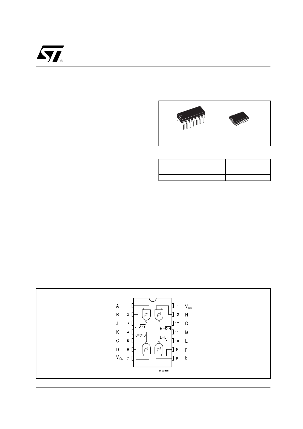
The HCF4093B is a m onolithic integrated circuit
fabricated in Metal Oxide Semiconductor
technology available in DIP and SOP packages.
DIP SOP
ORDER CODES
PACKAGE TUBE T & R
DIP HCF4093BEY
SOP HCF4093BM1 HCF4093M013TR
The HCF4093B type consists of four schmitt
trigger circuits. Each circuit functions as a two
input NAND gate with schmitt trigger action on
both inputs. The gate switches at different points
for positive and negative going signals. The
difference between the positive voltage (V
the negative voltage (V
voltage (V
).
H
) is defined as hysteresis
N
) and
P
PIN CONNECTION
1/7September 2001
Page 2
HCF4093B
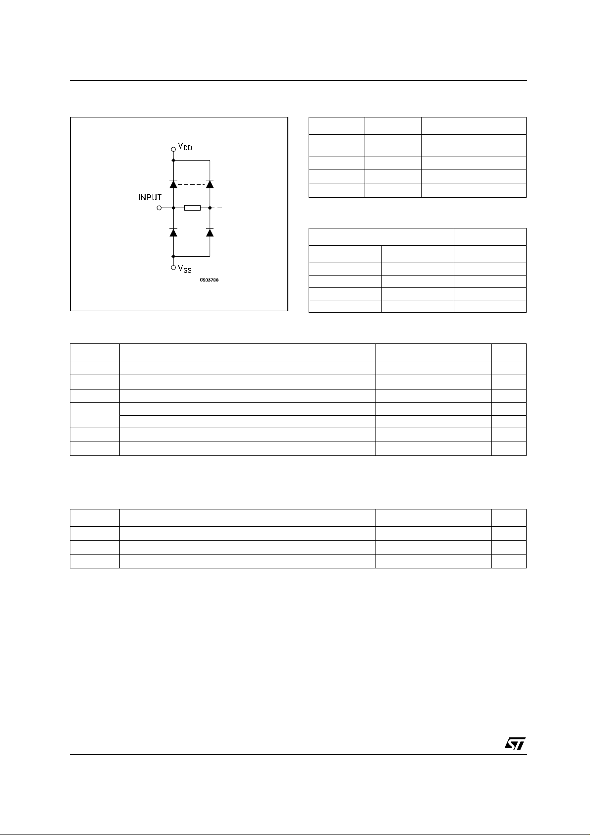
INPUT EQUIVALENT CIRCUIT PIN DESCRIPTION
PIN No SYMBOL NAME AND FUNCTION
1, 2, 5, 6, 8,
9, 12, 13
3, 4, 10, 11 J, K, L, M Data Outputs
7
14
TRUTH TABLE
A, C, E, G B, D, F, H J, K, L, M
ABSOLUTE MAXIMUM RATINGS
Symbol Parameter Value Unit
V
V
P
T
T
Absolute Maximum Ratings are those values beyond which damage to the device may occur. Functional operation under these conditions is
not implied.
All voltage values are referr ed to V
Supply Voltage
DD
DC Input Voltage -0.5 to VDD + 0.5
I
I
DC Input Current
I
Power Dissipation per Package 200 mW
D
Power Dissipation per Output Transistor 100 mW
Operating Temperature
op
Storage Temperature
stg
pin voltage.
SS
A, B, C, D, E,
F, G, H
V
SS
V
DD
Data Inputs
Negative Supply Voltage
Positive Supply Voltage
INPUTS OUTPUTS
LLH
LHH
HLH
HHL
-0.5 to +22 V
V
± 10 mA
-55 to +125 °C
-65 to +150 °C
RECOMMENDED OPERATING CONDITIONS
Symbol Parameter Value Unit
V
V
T
2/7
Supply Voltage
DD
Input Voltage 0 to V
I
Operating Temperature
op
3 to 20 V
DD
-55 to 125 °C
V
Page 3
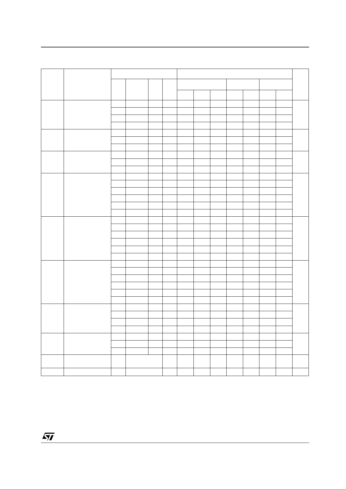
DC SPECIFICATIONS
Test Condition Value
T
Symbol Parameter
I
Quiescent Current 0/5 5 0.02 1 30 30
L
V
(V)
V
I
(V)
|I
|
O
O
(µA)
V
DD
(V)
= 25°C
A
Min. Typ. Max. Min. Max. Min. Max.
0/10 10 0.02 2 60 60
0/15 15 0.02 4 120 120
0/20 20 0.04 20 600 600
V
High Level Output
OH
Voltage
0/5 <1 5 4.95 4.95 4.95
0/15 <1 15 14.95 14.95 14.95
Low Level Output
V
OL
Voltage
5/0 <1 5 0.05 0.05 0.05
15/0 <1 15 0.05 0.05 0.05
Positive Trigger
V
P
Threshold Voltage
a 5 2.2 2.9 3.6 2.2 3.6 2.2 3.6
a 10 4.6 5.9 7.1 4.6 7.1 4.6 7.1
a 15 6.8 8.8 10.8 6.8 10.8 6.8 10.8
b 5 2.6 3.3 4.0 2.6 4 2.6 4
b 10 5.6 7 8.2 5.6 8.2 5.6 8.2
b 15 6.3 9.4 12.7 6.3 12.7 6.3 12.7
Negative Trigger
V
N
Threshold Voltage
a 5 0.9 1.9 2.8 0.9 2.8 0.9 2.8
a 10 2.5 3.9 5.2 2.5 5.2 2.5 5.2
a 15 4 5.8 7.4 4 7.4 4 7.4
b 5 1.4 2.3 3.2 1.4 3.2 1.4 3.2
b 10 3.4 5.1 6.6 3.4 6.6 3.4 6.6
b 15 4.8 7.3 9.6 4.8 9.6 4.8 9.6
Hysteresis Voltage a 5 0.3 0.9 1.6 0.3 1.6 0.3 1.6
V
H
a 10 1.2 2.3 3.4 1.2 3.4 1.2 3.4
a 15 1.6 3.5 5 1.6 5 1.6 5
b 5 0.3 0.9 1.6 0.3 1.6 0.3 1.6
b 10 1.2 2.3 3.4 1.2 3.4 1.2 3.4
b 15 1.6 3.5 5 1.6 5 1.6 5
I
OH
Output Drive
Current
0/5 2.5 <1 5 -1.36 -3.2 -1.15 -1.1
0/5 4.6 <1 5 -0.44 -1 -0.36 -0.36
0/10 9.5 <1 10 -1.1 -2.6 -0.9 -0.9
0/15 13.5 <1 15 -3.0 -6.8 -2.4 -2.4
I
OL
Output Sink
Current
0/5 0.4 <1 5 0.44 1 0.36 0.36
0/15 1.5 <1 15 3.0 6.8 2.4 2.4
Input Leakage
I
I
Current
C
Input Capacitance
I
The Noi se Margin fo r both "1" and "0" level is: 1V m i n. with VDD=5V, 2V min. with VDD=10V, 2.5V min. with VDD=15V
a : Input on terminals 1, 5, 8, 12 or 2, 6, 9, 13 ; ot her inputs t o V
b : Input on terminals 1 an d 2, 5 and 6, 8 and 9, or 12 and 13; oth er i nputs to V
0/18 Any Input 18
Any Input 5 7.5 pF
.
DD
DD
±10
.
-5
-40 to 85°C -55 to 125°C
±0.1 ±1 ±1 µA
HCF4093B
Unit
µA
V0/10 <1 10 9.95 9.95 9.95
V10/0 <1 10 0.05 0.05 0.05
V
V
V
mA
mA0/10 0.5 <1 10 1.1 2.6 0.9 0.9
3/7
Page 4
HCF4093B
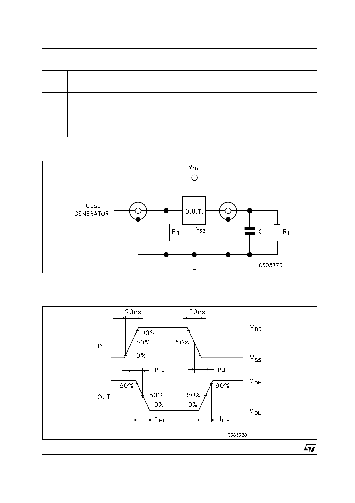
DYNAMIC ELECTRICAL CHARACTERISTICS (T
Symbol Parameter
t
PLH tPHL
t
TLH tTHL
(*) Typical temperature coefficient for a ll VDD value is 0.3 %/°C.
Propagation Delay Time 5 190 380
Output Transition Time 5 100 200
(V)
V
DD
15 65 130
15 40 80
TEST CIRCUIT
= 25°C, CL = 50pF, RL = 200KΩ, tr = tf = 20 ns)
amb
Test Condition Value (*) Unit
Min. Typ. Max.
ns10 90 180
ns10 50 100
CL = 50pF or equivalent (in cludes jig and probe capaci tance)
R
= 200KΩ
L
= Z
R
of pulse generator (typically 50Ω)
T
OUT
WAVEFORM : PROPAGATION DELAY TIMES (f=1MHz; 50% duty cycle)
4/7
Page 5

HCF4093B
Plastic DIP-14 MECHANICAL DATA
mm. inch
DIM.
MIN. TYP MAX. MIN. TYP. MAX.
a1 0.51 0.020
B 1.39 1.65 0.055 0.065
b 0.5 0.020
b1 0.25 0.010
D 20 0.787
E 8.5 0.335
e 2.54 0.100
e3 15.24 0.600
F 7.1 0.280
I 5.1 0.201
L 3.3 0.130
Z 1.27 2.54 0.050 0.100
P001A
5/7
Page 6
HCF4093B
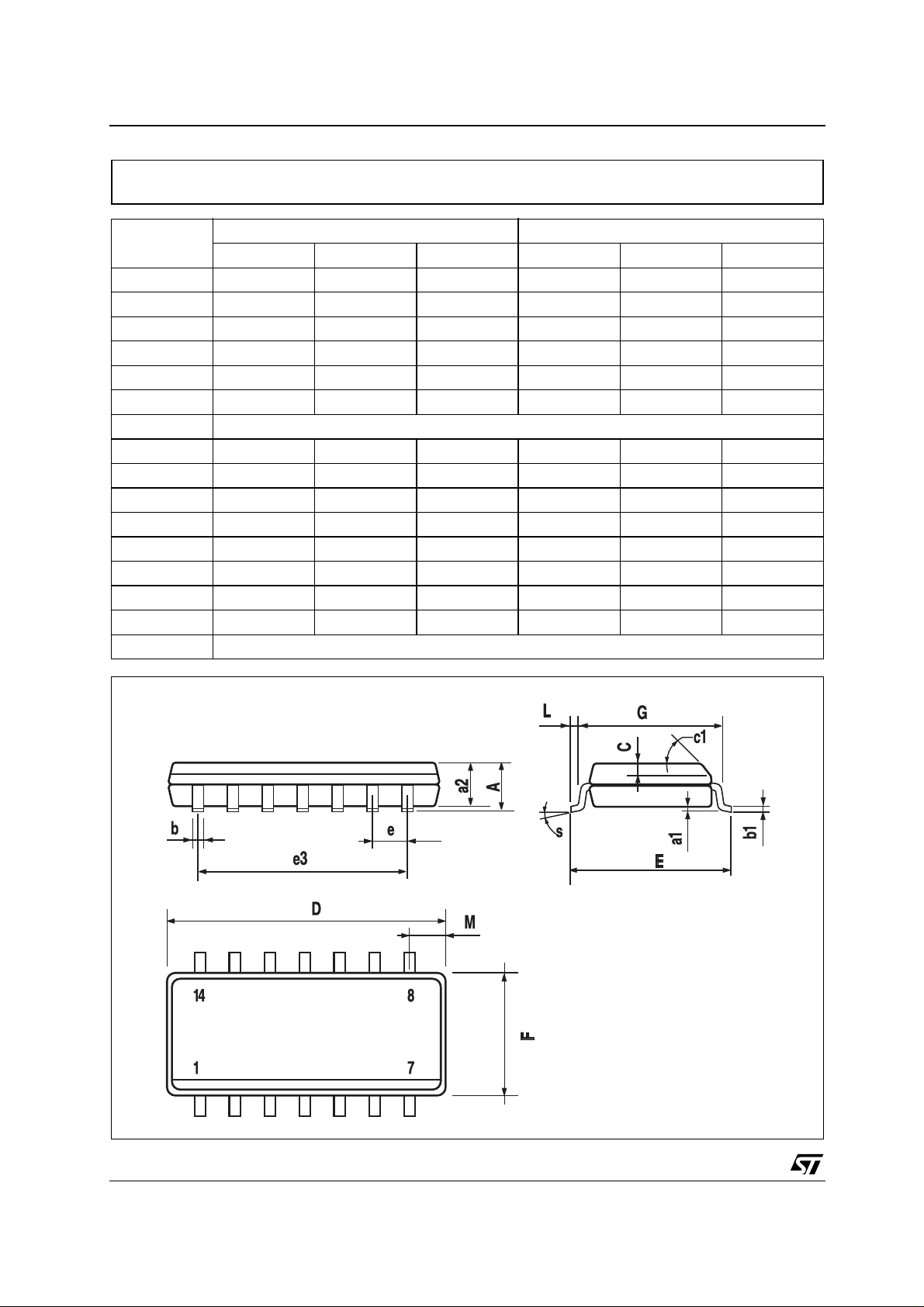
SO-14 MECHANICAL DATA
DIM.
A 1.75 0.068
a1 0.1 0.2 0.003 0.007
a2 1.65 0.064
b 0.35 0.46 0.013 0.018
b1 0.19 0.25 0.007 0.010
C 0.5 0.019
c1 45° (typ.)
D 8.55 8.75 0.336 0.344
E 5.8 6.2 0.228 0.244
e 1.27 0.050
e3 7.62 0.300
F 3.8 4.0 0.149 0.157
G 4.6 5.3 0.181 0.208
L 0.5 1.27 0.019 0.050
M 0.68 0.026
S8° (max.)
MIN. TYP MAX. MIN. TYP. MAX.
mm. inch
6/7
PO13G
Page 7

HCF4093B
Information furnished is bel ieved to be accurate and reliable. However, STMicroe lectronics assumes no responsibility for the
consequences of use of such information nor for any infringement of patents or other rights of third parties which may result from
its use. No li cense is granted by implication or otherwise unde r any patent or patent rights of STMicroelectronics. Specifications
mentioned in this publication ar e subject to change without notice. This publication supersedes and replaces all information
previously supplied. S TMicroelectronics products are not authorized for use as critica l components in life suppo rt devices or
systems without express written approval of STMicroelectronics.
Australi a - Brazil - Chi na - Finlan d - F rance - Germany - Hong Kong - India - Ital y - Japan - Ma l aysia - Malta - Morocco
© The ST logo is a registered trademark of STMicroelectronics
© 2001 STM icroelectronics - Pr inted in Ital y - All Rights Reserved
STMicr o el ectronics GROUP OF COMPA NI E S
Singapo re - Spain - Sweden - Swit zerland - Un i ted Kingdom
© http://www.st.com
7/7
 Loading...