

Features
■ Schmidt trigger action on each input with no
external components
■ Hysteresis voltage typically 0.9 V at V
and 2.3 V at V
■ Noise immunity greater than 50% of V
■ No limit on input rise and fall times
■ Quiescent current specified up to 20 V
■ Standardized symmetrical output
DD
=10 V
characteristics
■ 5 V, 10 V and 15 V parametric ratings
■ Input leakage current
■ I
= 100 nA (max) at VDD=18V TA=25°C
I
■ 100% tested for quiescent current
■ Meets all requirements of JEDEC JESD13B
"Standard Specifications for Description of B
Series CMOS Devices"
DD
DD
=5V
(typ.)
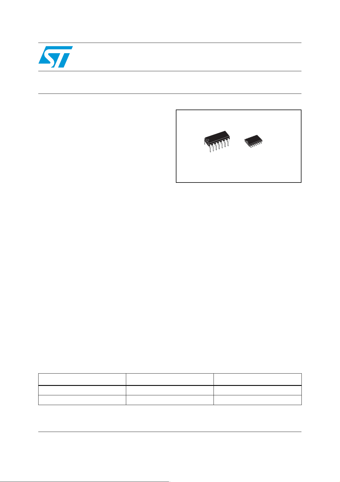
HCF4093
QUAD 2-input NAND Schmidt trigger
DIP-14
Description
The HCF4093 is a monolithic integrated circuit
fabricated in metal oxide semiconductor
technology available in DIP and SOP packages.
The HCF4093 type consists of 4 schmitt trigger
circuits. Each circuit functions has a 2-input
NAND gate with schmitt trigger action on both
inputs. The gate switches at different points for
positive and negative going signals. The
difference between the positive voltage (V
the negative voltage (V
voltage (V
).
H
SOP-14
) and
) is defined as hysteresis
N
P
Table 1. Device summary
Order code Package Packaging
HCF4093BEY DIP-14 Tube
HCF4093M013TR SOP-14 Tape and Reel
August 2007 Rev 2 1/13
www.st.com
13
Pin settings HCF4093
1 Pin settings
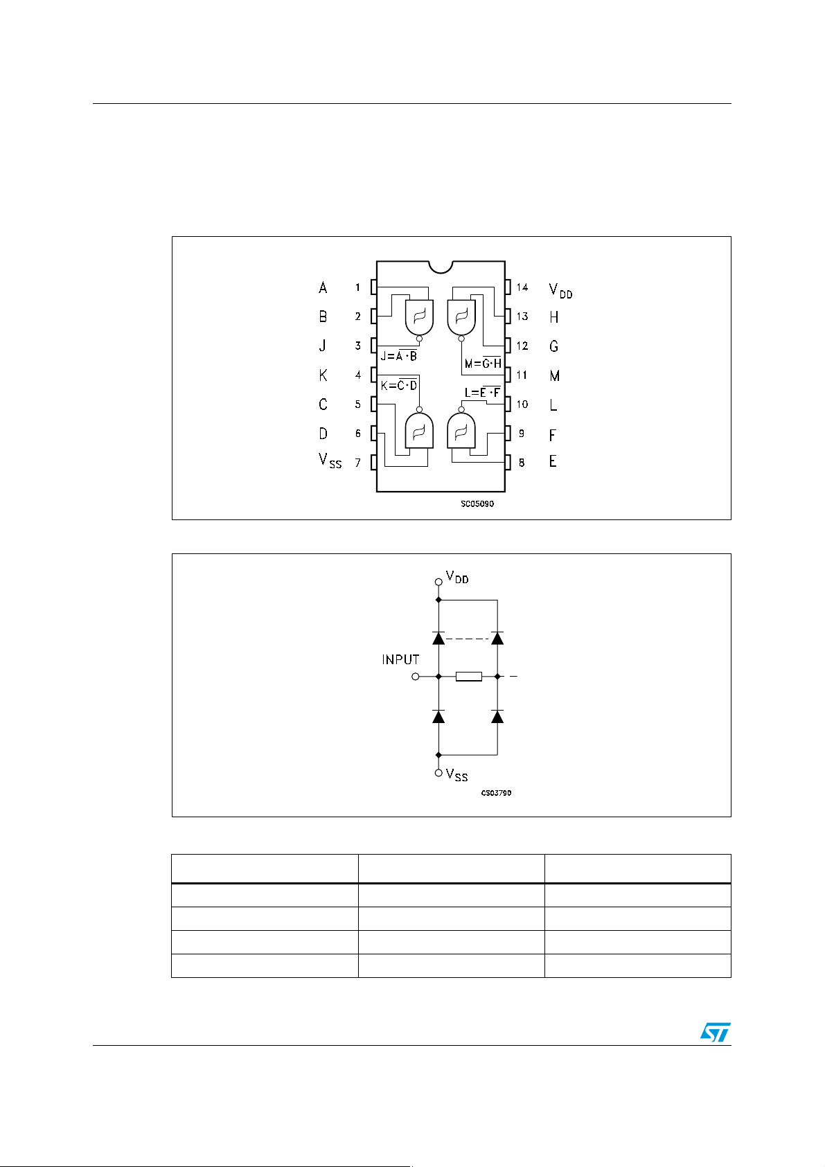
1.1 Pin connection
Figure 1. HCF4093B pin connection
Figure 2. Input equivalent circuit
Table 2. Pin description
Pin number Symbol Name and function
1, 2, 5, 6, 8, 9, 12, 13 A, B, C, D, E, F, G, H Data Inputs
3, 4, 10, 11 J, K, L, M Data Outputs
7V
14 V
SS
DD
Negative Supply Voltage
Positive Supply Voltage
2/13
HCF4093 Pin settings
Table 3. Truth table
Inputs Outputs
A, C, E, G B, D, F, H J, K, L, M
LLH
LHH
HLH
HHL
3/13
Maximum ratings HCF4093
2 Maximum ratings
Stressing the device above the rating list ed in the “Absolute Maximum Ratings” table may
cause permanent damage to the device. These are stress ratings only and operation of the
device at these or any ot her conditions above those indicated in the Operating sections of
this specification is not implied. Exposure to Absolute Maximum Rating conditions for
extended periods may aff ect device reliability. Refer also to the STMicroelectronics SURE
Program and other relevant quality documents.
Table 4. Absolute maximum ratings
Symbol Parameter Value Unit
V
Supply voltage -0.5 to + 22 V
DD
DC Input voltage -0.5 to VDD + 0.5 V
V
I
I
DC Input current ± 10 mA
I
Power dissipation per package 200 mW
P
D
Power dissipation per output transistor 100 mW
T
T
Operating temperature -55 to +125 °C
op
Storage temperature -65 to +150 °C
stg
2.1 Recommended operating conditions
Table 5. Recommended operating conditions
Symbol Parameter Value Unit
V
DD
V
I
T
op
Supply voltage 3 to 20 V
Input voltage 0 to V
Operating temperature -55 to 125 °C
DD
V
4/13
HCF4093 Electrical characteristics
3 Electrical characteristics
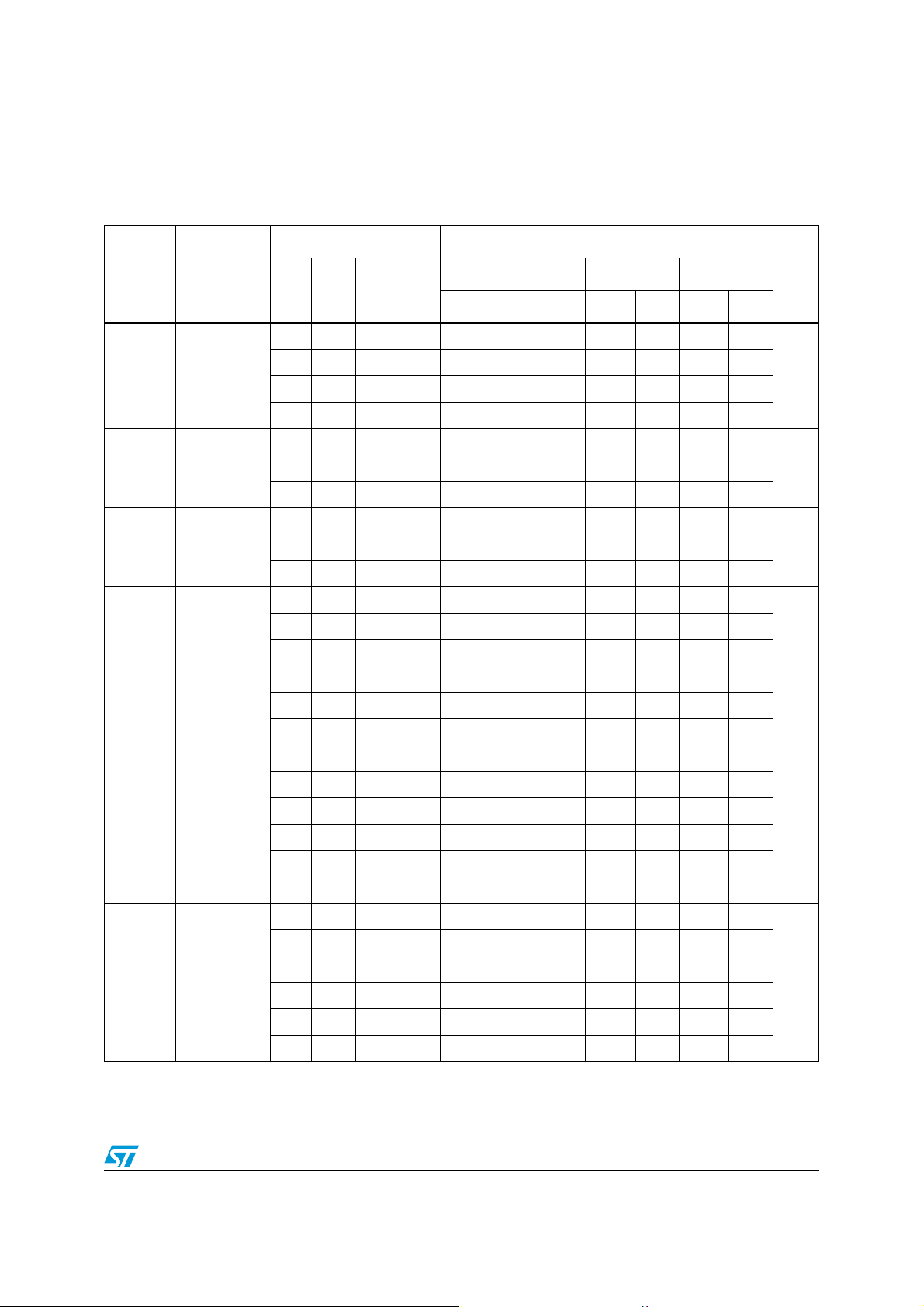
Table 6. DC specification
Symbol Parameter
V
I
(V)
0/5 5 0.02 1 30 30
I
L
Quiescent
current
0/10 10 0.02 2 60 60
0/15 15 0.02 4 120 120
0/20 20 0.04 20 600 600
High level
V
OH
output
voltage
Low level
OL
output
V
voltage
0/5 <1 5 4.95 4.95 4.95
0/15 <1 15 14.95 14.95 14.95
5/0 <1 5 0.05 0.05 0.05
15/0 <1 15 0.05 0.05 0.05
a 5 2.2 2.9 3.6 2.2 3.6 2.2 3.6
a 10 4.6 5.9 7.1 4.6 7.1 4.6 7.1
Positive
a 15 6.8 8.8 10.8 6.8 10.8 6.8 10.8
b 5 2.6 3.3 4.0 2.6 4 2.6 4
P
trigger
threshold
V
voltage
b 10 5.6 7 8.2 5.6 8.2 5.6 8.2
Test Cond iti on Value
= 25°C -40 to 85°C -55 to 125°C
T
V
(V)
|IO|
(μA)
V
DD
(V)
O
A
Min Typ Max Min Max Min Max
Unit
μA
V0/10 <1 10 9.95 9.95 9.95
V10/0 <1 10 0.05 0.05 0.05
V
b 15 6.3 9.4 12.7 6.3 12.7 6.3 12.7
a 5 0.9 1.9 2.8 0.9 2.8 0.9 2.8
a 10 2.5 3.9 5.2 2.5 5.2 2.5 5.2
Negative
a 15 4 5.8 7.4 4 7.4 4 7.4
V
b 5 1.4 2.3 3.2 1.4 3.2 1.4 3.2
N
trigger
threshold
V
voltage
b 10 3.4 5.1 6.6 3.4 6.6 3.4 6.6
b 15 4.8 7.3 9.6 4.8 9.6 4.8 9.6
a 5 0.3 0.9 1.6 0.3 1.6 0.3 1.6
a 10 1.2 2.3 3.4 1.2 3.4 1.2 3.4
a 15 1.6 3.5 5 1.6 5 1.6 5
V
b 5 0.3 0.9 1.6 0.3 1.6 0.3 1.6
H
Hysteresis
voltage
V
b 10 1.2 2.3 3.4 1.2 3.4 1.2 3.4
b 15 1.6 3.5 5 1.6 5 1.6 5
5/13
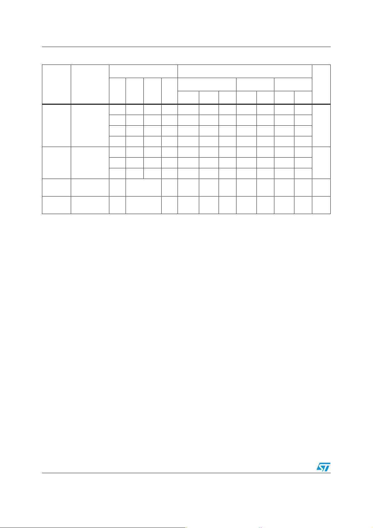
Electrical characteristics HCF4093
Table 6. DC specification (continued)
Test Cond iti on Value
Symbol Parameter
OH
OL
I
C
I
I
Output drive
current
Output sink
current
Input leakage
current
Input
capacitance
1. The noise margin for both "1" and "0" level is: 1 V min. with VDD= 5 V, 2 V min. with VDD=10V, 2.5V min
with VDD=15V
a: Input on terminals 1, 5, 8, 12 or 2, 6, 9, 13; other inputs to V
b: Input on terminals 1 and 2, 5 and 6, 8 and 9, or 12 and 13; other inputs to V
I
I
= 25°C -40 to 85°C -55 to 125°C
T
V
(V)
V
|IO|
I
O
(V)
(μA)
V
DD
(V)
A
Min Typ Max Min Max Min Max
0/5 2.5 <1 5 -1.36 -3.2 -1.15 -1.1
0/5 4.6 <1 5 -0.44 -1 -0.36 -0.36
0/10 9.5 <1 10 -1.1 -2.6 -0.9 -0.9
0/15 13.5 <1 15 -3.0 -6.8 -2.4 -2.4
0/5 0.4 <1 5 0.44 1 0.36 0.36
0/15 1.5 <1 15 3.0 6.8 2.4 2.4
-5
0/18 Any Input 18 ±10
±0.1 ±1 ±1 μA
Any Input 5 7.5 pF
.
DD
.
DD
Unit
mA
mA0/10 0.5 <1 10 1.1 2.6 0.9 0.9
6/13
HCF4093 Electrical characteristics
3.1 Dynamic electrical characteristics
)
Table 7. Dynamic electrical characteris tics (T
t
=20ns)
r=tf
Condition
Symbol Parameter
t
PLH tPHL
t
TLH tTHL
Propagation delay time
Output transition time
= 25°C, CL=50pF, RL= 200 KΩ,
amb
Test
V
DD
(V)
Value (*) Unit
Min Typ Max
5 190 380
15 65 130
5 100 200
15 40 80
ns10 90 180
ns10 50 100
(*) Typical temperature coefficient for all V
value is 0.3 %/°C.
DD
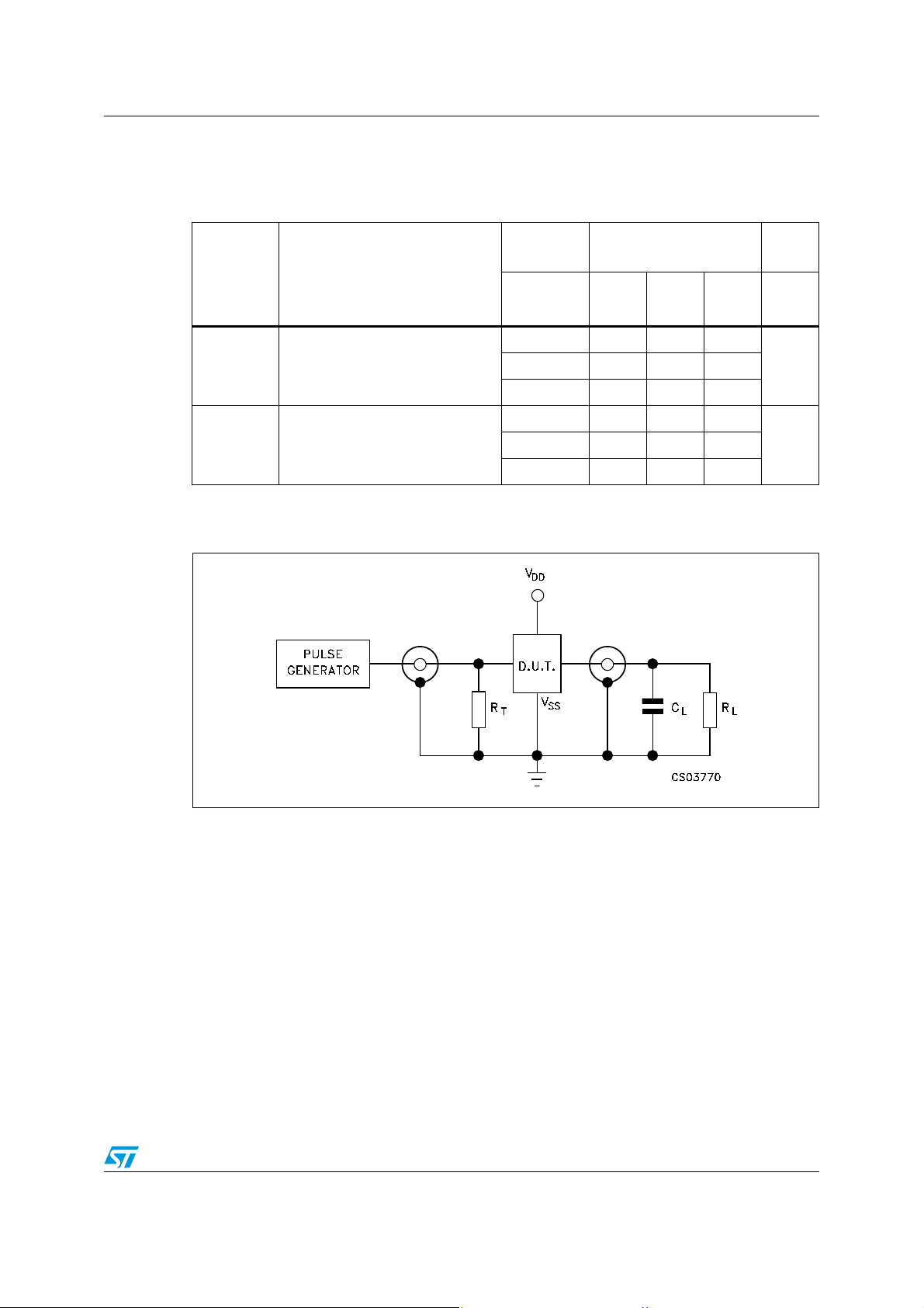
Figure 3. T est circuit
1. CL= 50 pF or equivalent (includes jig and probe capacitance)
=200KΩ
2. R
L
=Z
3. R
T
of pulse generator (typically 50 Ω)
OUT
7/13

Electrical characteristics HCF4093
Figure 4. Waveform: propagation delay times (f = 1 MHz; 50% duty cycle)
8/13

HCF4093 Package mechanical data
4 Package mechanical data
In order to meet environmental requirements, ST offers these devices in ECOPACK®
packages. These packages have a Lead-free second level interconnect. The category of
second level interconnect is marked on the package and on the inner box label, in
compliance with JEDEC Standard JESD97. The maximum ratings related t o soldering
conditions are also marked on the inner box label. ECOPACK is an ST trademark.
ECOPACK specifications are available at: www.st.com.
Figure 5. Plastic DIP-14 package outline
P001A
1. Drawing not to scale.
Table 8. Plastic DIP-14 mechanical data
millimeters inches
Symbol
Min Typ Max Min Typ Max
a1 0.51 0.020
B 1.39 1.65 0.055 0.065
b0.5 0.020
b1 0.25 0.010
D200.787
E8.5 0.335
e 2.54 0.100
e3 15.24 0.600
F 7.1 0.280
I 5.1 0.201
L3.3 0.130
Z 1.27 2.54 0.050 0.100
9/13

Package mechanical data HCF4093
Figure 6. SO-14 package outline
PO13G
1. Drawing not to scale.
Table 9. SO-14 mechanical data
millimeters inches
Symbol
Min Typ Max Min Typ Max
A1.750.068
a1 0.1 0.2 0.003 0.007
a2 1.65 0.064
b 0.35 0.46 0.013 0.018
b1 0.19 0.25 0.007 0.010
C0.5 0.019
c1 45°(typ.)
D 8.55 8.75 0.336 0.344
E 5.8 6.2 0.228 0.244
e 1.27 0.050
e3 7.62 0.300
F 3.8 4.0 0.149 0.157
G 4.6 5.3 0.181 0.208
L 0.5 1.27 0.019 0.050
M0.680.026
S 8°(max.)
10/13
HCF4093 Package mechanical data
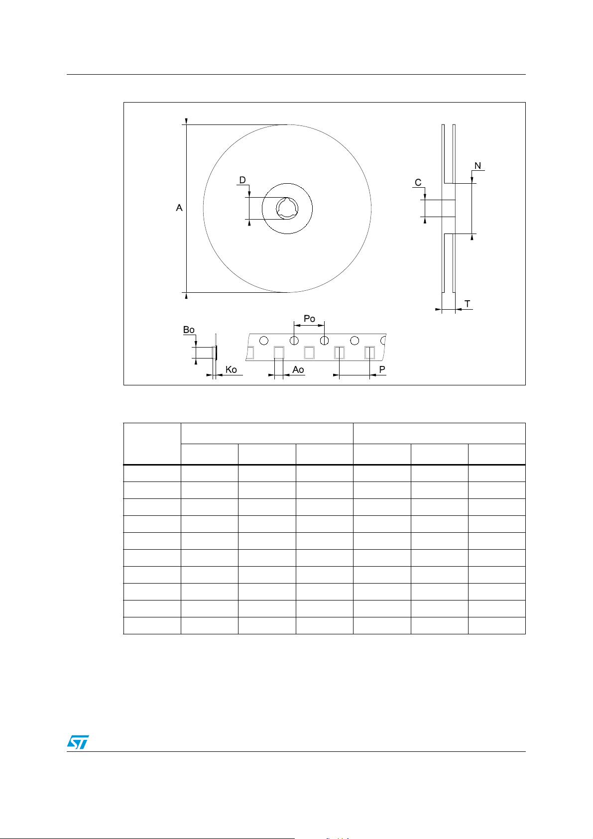
Figure 7. SO-14 tape and reel information
1. Drawing not to scale.
Table 10. SO-14 tape and reel information
millimeters inches
Symbol
Min Typ Max Min Typ Max
A 330 12.992
C 12.8 13.2 0.504 0.519
D 20.2 0.795
N60 2.362
T22.40.882
Ao 6.4 6.6 2.252 0.260
Bo 9 9.2 0.354 0.362
Ko 2.1 2.3 0.082 0.090
Po 3.9 4.1 0.153 0.161
P 7.9 8.1 0.311 0.319
11/13

Revision history HCF4093
5 Revision history
Table 11. Document re vision history
Date Revision Changes
Sept-2001 1 First release
Document converted to new ST template, added Figure 7: SO-14
16-Aug-2007 2
tape and reel information on page 11 andTable 10: SO-14 tape and
reel information on page 11, small text changes.
12/13

HCF4093
Please Read Carefully:
Information in this document is provided solely in connection with ST products. STMicroelectronics NV and its subsidiaries (“ST”) reserve the
right to make changes, corrections, modifications or improvements, to this document, and the products and services described herein at any
time, without notice.
All ST products are sold pursuant to ST’s terms and conditions of sale.
Purchasers are solely res ponsibl e fo r the c hoic e, se lecti on an d use o f the S T prod ucts and s ervi ces d escr ibed he rein , and ST as sumes no
liability whatsoever relati ng to the choice, selection or use of the ST products and services described herein.
No license, express or implied, by estoppel or otherwise, to any intellectual property rights is granted under this document. If any part of this
document refers to any third pa rty p ro duc ts or se rv ices it sh all n ot be deem ed a lice ns e gr ant by ST fo r t he use of su ch thi r d party products
or services, or any intellectua l property c ontained the rein or consi dered as a warr anty coverin g the use in any manner whats oever of suc h
third party products or servi ces or any intellectual property contained therein.
UNLESS OTHERWISE SET FORTH IN ST’S TERMS AND CONDITIONS OF SALE ST DISCLAIMS ANY EXPRESS OR IMPLIED
WARRANTY WITH RESPECT TO THE USE AND/OR SALE OF ST PRODUCTS INCLUDING WITHOUT LIMITATION IMPLIED
WARRANTIES OF MERCHANTABILITY, FITNESS FOR A PARTICUL AR PURPOS E (AND THEIR EQUIVALE NTS UNDER THE LAWS
OF ANY JURISDICTION), OR INFRINGEMENT OF ANY PATENT, COPYRIGHT OR OTHER INTELLECTUAL PROPERTY RIGHT.
UNLESS EXPRESSLY APPROVED IN WRITING BY AN AUTHORIZED ST REPRESENTATIVE, ST PRODUCTS ARE NOT
RECOMMENDED, AUTHORIZED OR WARRANTED FOR USE IN MILITARY, AIR CRAFT, SPACE, LIFE SAVING, OR LIFE SUSTAINING
APPLICATIONS, NOR IN PRODUCTS OR SYSTEMS WHERE FAILURE OR MALFUNCTION MAY RESULT IN PERSONAL INJ URY,
DEATH, OR SEVERE PROPERTY OR ENVIRONMENTAL DAMAGE. ST PRODUCTS WHICH ARE NOT SPECIFIED AS "AUTOMOTIVE
GRADE" MAY ONLY BE USED IN AUTOMOTIVE APPLICATIONS AT USER’S OWN RISK.
Resale of ST products with provisions different from the statements and/or technical features set forth in this document shall immediately void
any warranty granted by ST fo r the ST pro duct or serv ice describe d herein and shall not cr eate or exten d in any manne r whatsoever , any
liability of ST.
ST and the ST logo are trademarks or registered trademarks of ST in various countries.
Information in this document su persedes and replaces all info rmation previously supplied.
The ST logo is a registered trademark of STMicroelectronics. All other names are the property of their respective owners.
© 2007 STMicroelectronics - All rights reserved
STMicroelectronics group of compan ie s
Australia - Belgium - Brazil - Canada - China - Czech Republic - Finland - France - Germany - Hong Kong - India - Israel - Italy - Japan -
Malaysia - Malta - Morocco - Singapore - Spain - Sweden - Switzerland - United Kingdom - United States of America
www.st.com
13/13
 Loading...