

ST HCF4081B User Manual
■ MEDIUM SPEED OPERATION:
t
= 60ns (Typ.) at 10V
PD
■ QUIESCENT CURRENT SPECIFIED UP TO
20V
■ 5V,10V AND 15V PARAMETRIC RATINGS
■ INPUT LEAKAGE CURRE NT
I
= 100nA (MAX) AT VDD=18VTA= 25°C
I
■ 100% TESTED FOR QUIESCENT CURRENT
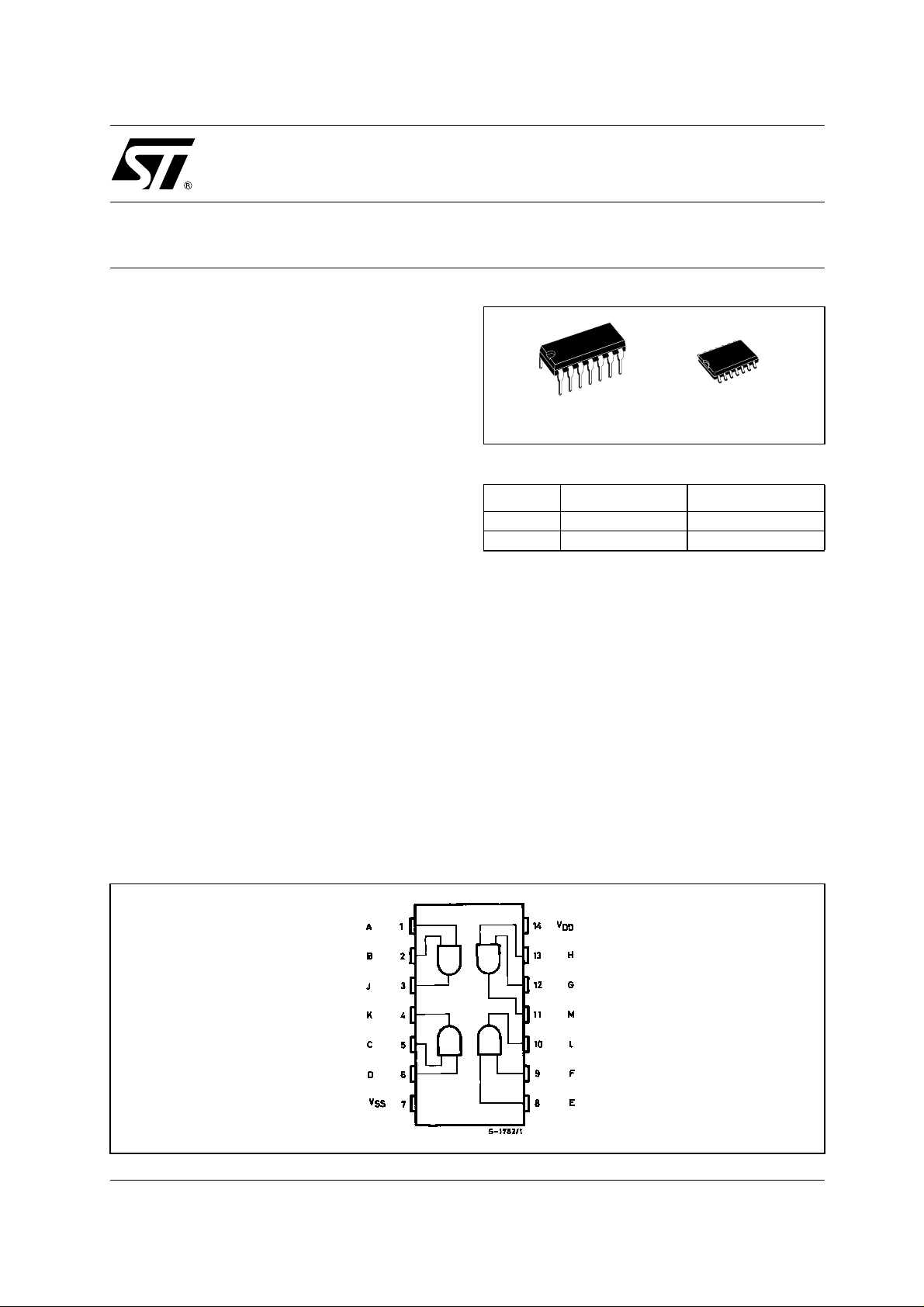
HCF4081B
QUAD 2 INPUT AND GATE
DIP SOP
DESCRIPTION
The HCF4081B is a monolithic integrated circuit
fabricated in Metal Oxide Semiconductor
technology available in DIP and SOP packages.
The HCF4081B QUAD 2 INPUT AND GATE
provide the system designer with direct
implementation of the AND function and
supplement the existing family of CMOS gates.
PIN CONNECTION
ORDER CODES
PACKAGE TUBE T & R
DIP HCF4081BEY
SOP HCF4081BM1 HCF4081M013TR
1/8March 2004
HCF4081B
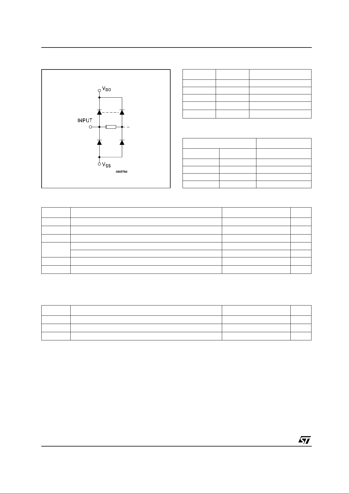
INPUT EQUIVALENT CIRCUIT PIN DESCRIP TION
PIN N° SYMBOL NAME AND FUNCTION
1, 5, 8, 12 A, C, E, G Data Inputs
2, 6, 9, 13 B, D, F, H Data Inputs
3, 4, 10, 11 J, K, L, M Data Outputs
7
14
TRUTH TABLE
INPUTS OUTPUTS
A,C,E,G B,D,F,H J,K,L,M
LL L
LH L
HL L
HH H
ABSOLUTE MAXIMUM RATINGS
Symbol Parameter Value Unit
V
V
P
T
T
stg
Absolute Maximum Ratings are those values beyond which damage to the device may occur. Functional operation under these conditions is
not implied.
All voltagevalues arereferred toV
Supply Voltage
DD
DC Input Voltage -0.5 to VDD+0.5
I
DC Input Current
I
I
Power Dissipation per Package 200 mW
D
Power Dissipation per Output Transistor 100 mW
Operating Temperature
op
Storage Temperature
pin voltage.
SS
V
SS
V
DD
Negative Supply Voltage
Positive Supply Voltage
-0.5 to +22 V
± 10 mA
-55 to +125 °C
-65 to +150 °C
V
RECOMMENDED OPERATING CONDITIONS
Symbol Parameter Value Unit
V
V
T
2/8
Supply Voltage
DD
Input Voltage 0 to V
I
Operating Temperature
op
3to20 V
DD
-55 to 125 °C
V
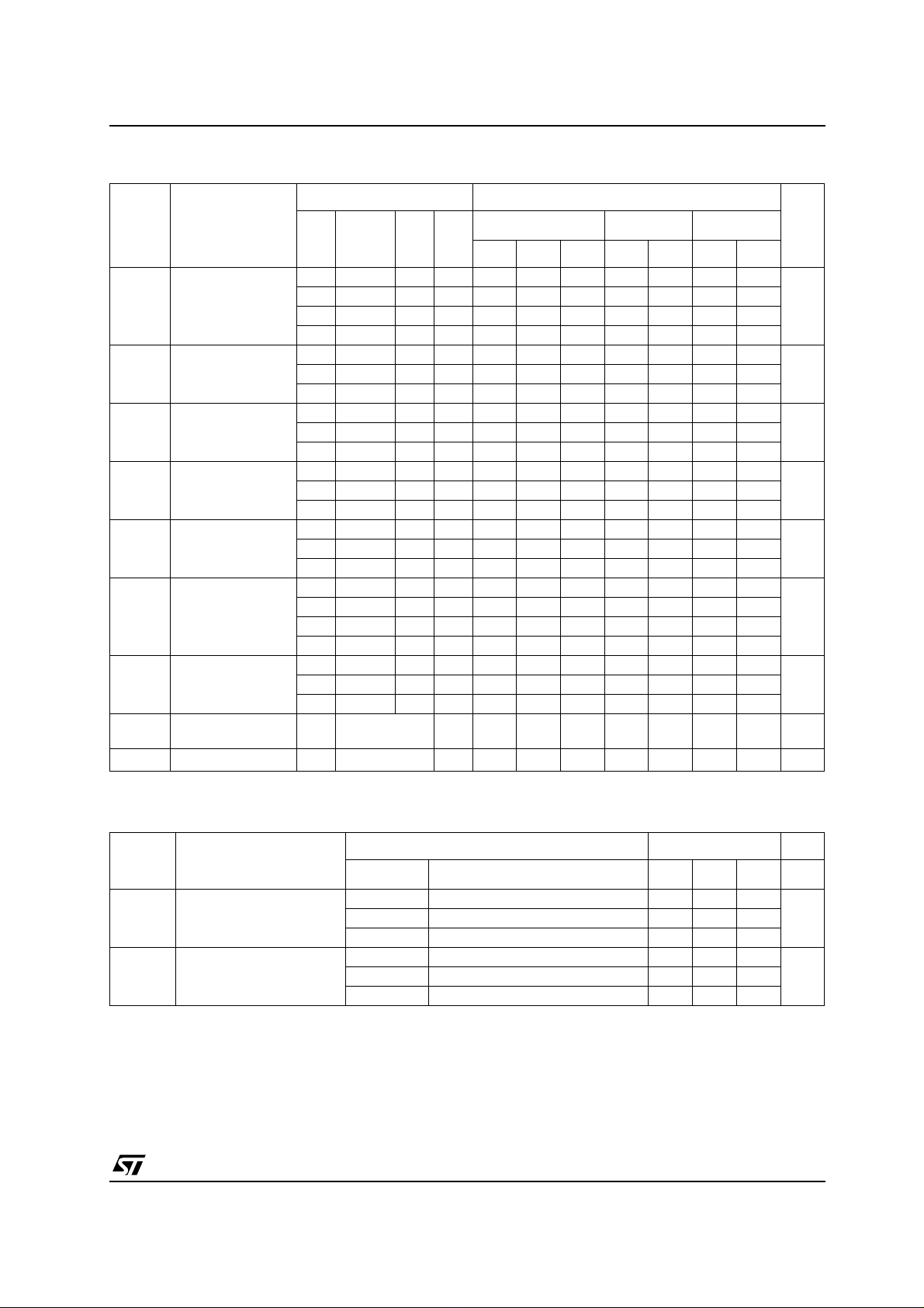
DC SPECIFICATIONS
Test Condition Value
T
Symbol Parameter
I
Quiescent Current 0/5 5 0.01 0.25 7.5 7.5
L
V
(V)
V
I
(V)
|I
|
O
O
(µA)
V
DD
(V)
= 25°C
A
Min. Typ. Max. Min. Max. Min. Max.
0/10 10 0.01 0.5 15 15
0/15 15 0.01 1 30 30
0/20 20 0.02 5 150 150
V
High Level Output
OH
Voltage
0/5 <1 5 4.95 4.95 4.95
0/15 <1 15 14.95 14.95 14.95
V
Low Level Output
OL
Voltage
5/0 <1 5 0.05 0.05 0.05
15/0 <1 15 0.05 0.05 0.05
V
High Level Input
IH
Voltage
0.5/4.5 <1 5 3.5 3.5 3.5
1.5/13.5 <1 15 11 11 11
V
Low Level Input
IL
Voltage
4.5/0.5 <1 5 1.5 1.5 1.5
13.5/1.5 <1 15 4 4 4
I
OH
Output Drive
Current
0/5 2.5 <1 5 -1.36 -3.2 -1.15 -1.1
0/5 4.6 <1 5 -0.44 -1 -0.36 -0.36
0/10 9.5 <1 10 -1.1 -2.6 -0.9 -0.9
0/15 13.5 <1 15 -3.0 -6.8 -2.4 -2.4
I
OL
Output Sink
Current
0/5 0.4 <1 5 0.44 1 0.36 0.36
0/15 1.5 <1 15 3.0 6.8 2.4 2.4
I
Input Leakage
I
Current
Input Capacitance
C
I
The Noise Margin forboth "1"and "0" level is:1V min. with VDD=5V, 2V min. with VDD=10V, 2.5V min. with VDD=15V
0/18 Any Input 18
Any Input 5 7.5 pF
±10
-5
-40 to 85°C -55 to 125°C
±0.1 ±1 ±1 µA
HCF4081B
Unit
µA
V0/10 <1 10 9.95 9.95 9.95
V10/0 <1 10 0.05 0.05 0.05
V1/9 <1 10 7 7 7
V9/1 <1 10 3 3 3
mA
mA0/10 0.5 <1 10 1.1 2.6 0.9 0.9
DYNAMIC ELECTRICAL CHARACTERISTICS (T
Symbol Parameter
t
PLHtPHL
t
TLHtTHL
(*) Typical temperature coefficient for all VDDvalue is 0.3%/°C.
PropagationDelay Time 5 125 250
Output TransitionTime 5 100 200
(V)
V
DD
15 45 90
15 40 80
= 25°C, CL= 50pF, RL= 200KΩ,tr=tf=20ns)
amb
Test Condition Value (*) Unit
Min. Typ. Max.
ns10 60 125
ns10 60 100
3/8
 Loading...