

Features
■ Medium-speed operation
t
= t
PHL
V
DD
■ Quiescent current specified up to 20 V
■ 5 V, 10 V and 15 V parametric ratings
■ Input leakage current
I
= 100 nA (max) at VDD = 18 V, TA = 25 °C
I
■ 100% tested for quiescent current
= 70 ns (typ) at CL = 50 pF and
PLH
= 10 V
Quad exclusive OR gate
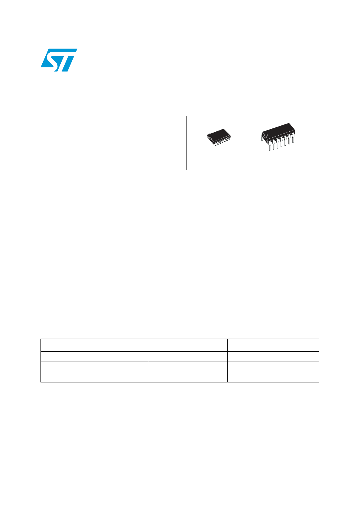
SO14
Description
HCF4070
Datasheet − production data
DIP14
Applications
■ Automotive
■ Industrial
■ Computer
■ Consumer
The HCF4070 is a monolithic integrated circuit
fabricated in Metal Oxide Semiconductor
technology available in DIP14 and SO14
packages.
The HCF4070 contains four independent
exclusive OR gates. This device provides the
system designer with a means for direct
implementation of the exclusive OR gate for
applications such as logical comparators,
adders/subtractors, parity generators and
checkers.
Table 1. Device summary
Order code Temperature range Package
HCF4070M013TR –55 °C to +125 °C SO14
HCF4070YM013TR
HCF4070BEY –55 °C to +125 °C DIP14
1. Qualification and characterization (according to AEC Q100 and Q003 or equivalent) and advanced screening (according to
AEC Q001 and Q002 or equivalent) are ongoing.
(1)
–40 °C to +125 °C SO14 (automotive grade)
June 2012 Doc ID 2061 Rev 4 1/11
This is information on a product in full production.
www.st.com
11
Device overview HCF4070
1 Device overview
Figure 1. Pin connections
Table 2. Pin description
Pin number Symbol/name Function
1, 5, 8, 12 A, C, E, G Data inputs
2, 6, 9, 13 B, D, F, H Data inputs
3, 4, 10, 11 J, K, L, M Data outputs
7V
14 V
Figure 2. Input equivalent circuit
SS
DD
Negative supply voltage
Positive supply voltage
2/11 Doc ID 2061 Rev 4
HCF4070 Device overview
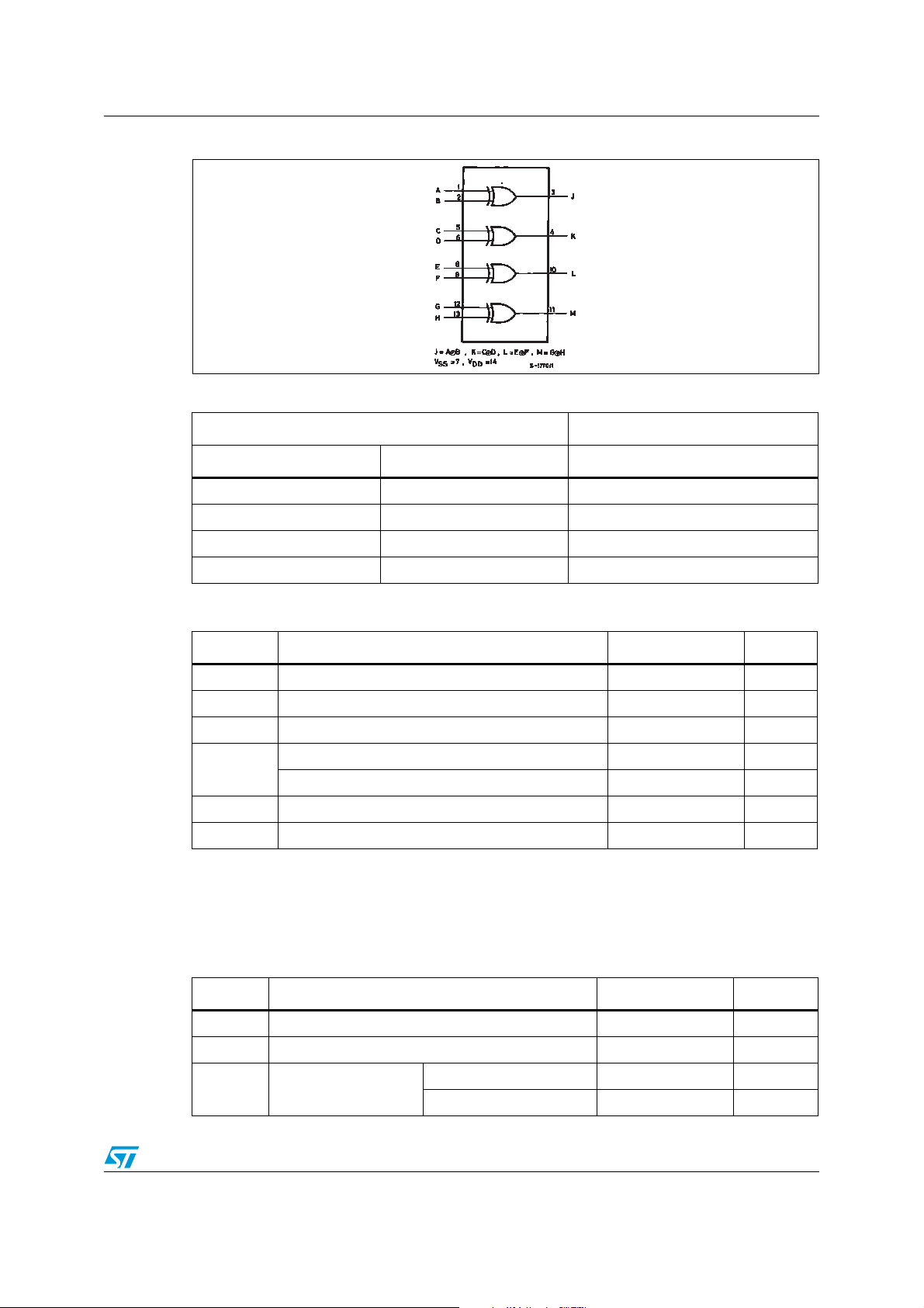
Figure 3. Logic diagram
Table 3. Truth table
Inputs Output
A, C, E, G B, D, F, H J, K, L, M
LL L
LH H
HL H
HH L
Table 4. Absolute maximum ratings
Symbol Parameter Value Unit
V
DD
V
I
I
Supply voltage -0.5 to +22 V
DC input voltage -0.5 to VDD + 0.5 V
I
DC input current ± 10 mA
Power dissipation per package 200 mW
P
D
T
op
T
stg
Power dissipation per output transistor 100 mW
Operating temperature -55 to +125 °C
Storage temperature -65 to +150 °C
Absolute maximum ratings are those values beyond which damage to the device may occur.
Functional operation under these conditions is not implied.
All voltage values are relative to the V
Table 5. Recommended operating conditions
Symbol Parameter Value Unit
pin voltage.
SS
V
DD
V
Supply voltage 3 to 20 V
Input voltage 0 to V
I
DD
V
SO14, DIP14 -55 to 125 °C
T
Operating temperature
op
SO14 (automotive grade) -40 to 125 °C
Doc ID 2061 Rev 4 3/11
Device overview HCF4070
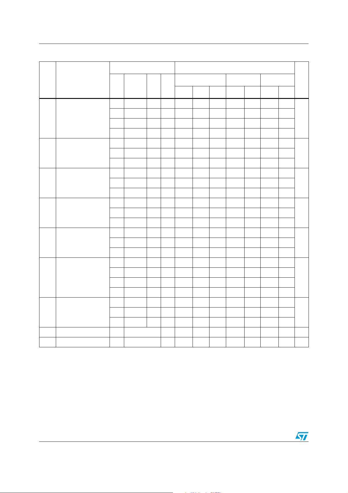
Table 6. DC specifications
Sym. Parameter
V
(V)
0/5 5 0.02 1 30 30
0/10 10 0.02 2 60 60
ILQuiescent current
0/15 15 0.02 4 120 120
0/20 20 0.04 20 600 600
0/5 <1 5 4.95 4.95 4.95
High-level output
V
OH
voltage
0/15 <1 15 14.95 14.95 14.95
5/0 <1 5 0.05 0.05 0.05
Low-level output
V
OL
voltage
15/0 <1 15 0.05 0.05 0.05
High-level input
V
IH
voltage
Low-level input
V
IL
voltage
0/5 2.5 <1 5 -1.36 -3.2 -1.15 -1.1
Test condition Value
V
I
(V)
|I
|
O
(μA)
V
DD
(V)
O
TA = 25°C -40 to 85°C -55 to 125°C
Min. Typ. Max. Min. Max. Min. Max.
0.5/4.5 <1 5 3.5 3.5 3.5
1.5/13.5 <1 15 11 11 11
4.5/0.5 <1 5 1.5 1.5 1.5
13.5/1.5 <1 15 4 4 4
Unit
μA
V0/10 <1 10 9.95 9.95 9.95
V10/0 <1 10 0.05 0.05 0.05
V1/9 <1 10 7 7 7
V9/1 <1 10 3 3 3
I
Output drive current
OH
0/10 9.5 <1 10 -1.1 -2.6 -0.9 -0.9
0/15 13.5 <1 15 -3.0 -6.8 -2.4 -2.4
0/5 0.4 <1 5 0.44 1 0.36 0.36
0/5 4.6 <1 5 -0.44 -1 -0.36 -0.36
Output sink current
I
OL
0/15 1.5 <1 15 3.0 6.8 2.4 2.4
IIInput leakage current 0/18 Any Input 18 ±10-5±0.1 ±1 ±1 μA
Input capacitance Any Input 5 7.5 pF
C
I
The noise margin for both the "1" and "0" level is: 1 V min. with V
V
= 10 V, 2.5 V min. with V
DD
DD
= 15 V.
= 5 V, 2 V min. with
DD
4/11 Doc ID 2061 Rev 4
mA
mA0/10 0.5 <1 10 1.1 2.6 0.9 0.9

HCF4070 Device overview
Table 7. Dynamic electrical characteristics
(T
= 25 °C, CL = 50 pF, RL = 200 kΩ, tr = tf = 20 ns)
amb
(1)
Unit
Symbol Parameter
Test condition Value
(V) Min. Typ. Max.
V
DD
5 140 280
t
PLH tPHL
Propagation delay time
ns10 70 130
15 50 100
5 100 200
t
TLH tTHL
Output transition time
ns10 50 100
15 40 80
1. Typical temperature coefficient for all VDD values is 0.3%/°C.
Figure 4. Test circuit
1. CL = 50 pF or equivalent (includes jig and probe capacitance)
= 200 kΩ
2. R
L
= Z
3. R
T
of pulse generator (typically 50 Ω)
OUT
Doc ID 2061 Rev 4 5/11

Device overview HCF4070
Figure 5. Waveform - propagation delay times (f = 1 MHz; 50% duty cycle)
6/11 Doc ID 2061 Rev 4

HCF4070 Package mechanical data
2 Package mechanical data
In order to meet environmental requirements, ST offers these devices in different grades of
ECOPACK
specifications, grade definitions and product status are available at: www.st.com.
ECOPACK
®
packages, depending on their level of environmental compliance. ECOPACK®
®
is an ST trademark.
Plastic DIP-14 MECHANICAL DATA
DIM.
MIN. TYP MAX. MIN. TYP. MAX.
020.015.01a
Z
hcni.mm
560.0550.056.193.1B
020.05.0b
010.052.01b
787.002D
533.05.8E
001.045.2e
006.042.513e
082
.01.7F
102.01.5I
031.03.3L
001.0050.045.272.1
P001A
Doc ID 2061 Rev 4 7/11

Package mechanical data HCF4070
SO-14 MECHANICAL DATA
DIM.
S
hcni.mm
MIN. TYP MAX. MIN. TYP. MAX.
910.05.0C
).pyt
( ˚541c
050.072.1e
003.026.73e
.0910.072.15.0L
).xam( ˚
8
860.057.1A
700.0300.02.01.01a
460.056.12a
810.0310.064.053.0b
010.0700.052.091.01b
443.0633.057.855.8D
442.0822.02.68.5E
751.0941.00.48.3F
802.0181.03.56.4G
050
620.086.0M
8/11 Doc ID 2061 Rev 4
PO13G

HCF4070 Package mechanical data
Tape & Reel SO-14 MECHANICAL DATA
DIM.
P
hcni.mm
MIN. TYP MAX. MIN. TYP. MAX.
597.02.02D
263.206N
90.0280.03.21.2oK
299.21033A
915.0405.02.318.21C
288.04.22T
062.0252.06.64.6oA
263.0453.02.99oB
0
161.0351.01.49.3oP
913.0113.01.89.7
Doc ID 2061 Rev 4 9/11

Revision history HCF4070
3 Revision history
Table 8. Document revision history
Date Revision Changes
Added Applications on page 1
11-Jun-2012 3
15-Jun-2012 4
Updated Table 1: Device summary
Revised document presentation, minor textual updates
Updated temperature range in Ta bl e 1
Updated T
in Ta bl e 4 and 5
op
10/11 Doc ID 2061 Rev 4

HCF4070
Please Read Carefully:
Information in this document is provided solely in connection with ST products. STMicroelectronics NV and its subsidiaries (“ST”) reserve the
right to make changes, corrections, modifications or improvements, to this document, and the products and services described herein at any
time, without notice.
All ST products are sold pursuant to ST’s terms and conditions of sale.
Purchasers are solely responsible for the choice, selection and use of the ST products and services described herein, and ST assumes no
liability whatsoever relating to the choice, selection or use of the ST products and services described herein.
No license, express or implied, by estoppel or otherwise, to any intellectual property rights is granted under this document. If any part of this
document refers to any third party products or services it shall not be deemed a license grant by ST for the use of such third party products
or services, or any intellectual property contained therein or considered as a warranty covering the use in any manner whatsoever of such
third party products or services or any intellectual property contained therein.
UNLESS OTHERWISE SET FORTH IN ST’S TERMS AND CONDITIONS OF SALE ST DISCLAIMS ANY EXPRESS OR IMPLIED
WARRANTY WITH RESPECT TO THE USE AND/OR SALE OF ST PRODUCTS INCLUDING WITHOUT LIMITATION IMPLIED
WARRANTIES OF MERCHANTABILITY, FITNESS FOR A PARTICULAR PURPOSE (AND THEIR EQUIVALENTS UNDER THE LAWS
OF ANY JURISDICTION), OR INFRINGEMENT OF ANY PATENT, COPYRIGHT OR OTHER INTELLECTUAL PROPERTY RIGHT.
UNLESS EXPRESSLY APPROVED IN WRITING BY TWO AUTHORIZED ST REPRESENTATIVES, ST PRODUCTS ARE NOT
RECOMMENDED, AUTHORIZED OR WARRANTED FOR USE IN MILITARY, AIR CRAFT, SPACE, LIFE SAVING, OR LIFE SUSTAINING
APPLICATIONS, NOR IN PRODUCTS OR SYSTEMS WHERE FAILURE OR MALFUNCTION MAY RESULT IN PERSONAL INJURY,
DEATH, OR SEVERE PROPERTY OR ENVIRONMENTAL DAMAGE. ST PRODUCTS WHICH ARE NOT SPECIFIED AS "AUTOMOTIVE
GRADE" MAY ONLY BE USED IN AUTOMOTIVE APPLICATIONS AT USER’S OWN RISK.
Resale of ST products with provisions different from the statements and/or technical features set forth in this document shall immediately void
any warranty granted by ST for the ST product or service described herein and shall not create or extend in any manner whatsoever, any
liability of ST.
ST and the ST logo are trademarks or registered trademarks of ST in various countries.
Information in this document supersedes and replaces all information previously supplied.
The ST logo is a registered trademark of STMicroelectronics. All other names are the property of their respective owners.
© 2012 STMicroelectronics - All rights reserved
STMicroelectronics group of companies
Australia - Belgium - Brazil - Canada - China - Czech Republic - Finland - France - Germany - Hong Kong - India - Israel - Italy - Japan -
Malaysia - Malta - Morocco - Philippines - Singapore - Spain - Sweden - Switzerland - United Kingdom - United States of America
www.st.com
Doc ID 2061 Rev 4 11/11
 Loading...