

HCF4067B
ANALOG SINGLE 16 CHANNEL
MULTIPLEXER/DEMULTIPLEXER
■ LOW ON RESISTANCE : 125Ω (Typ.) OVER
15V p-p SIGNAL INPUT RANGE FOR
V
- VSS = 15V
DD
■ HIGH OFF RESISTANCE : CHANNEL
LEAKAGE OF 10pA (Typ.) at
V
- VSS = 10V
DD
■ MATCHED SWITCH CHARACTERISTICS :
∆R
= 5Ω (Typ.) FOR VDD - VSS =15V
ON
■ VERY LOW QUIESCENT POWER
DISSIPATION UNDER A DIGITAL CONTROL
INPUT AND SUPPLY CONDITIONS : 0.2
(Typ.) at V
■ BINARY ADDR ESS D ECODING ON CHIP
■ QUIESCENT CURRENT SPECIFIED UP TO
- VSS = 10V
DD
µW
20V
■ STANDARDIZED SYMMETRICAL OUTPUT
CHARACTERISTICS
■ 5V, 10V AND 15V PARAMETRIC RATINGS
■ INPUT LEAKAGE CURRENT
I
= 100nA (MAX) AT VDD = 18V TA = 25°C
I
■ 100% TESTED FOR QUIESCENT CURRENT
■ MEETS ALL REQUIREMENTS OF JEDEC
JESD13B "STANDA RD SPECIFICATIONS
FOR DESCRIPTI ON OF B SERI ES CMOS
DEVICES"
SOP
ORDER CODES
PACKAGE TUBE T & R
SOP HCF4067BM1 HCF4067M013TR
HCF4067B, analog multiplexer/demultiplexer
CMOS, is a digitally controlled analog switches
device having low ON impedance, low OFF
leakage current and internal address decodin g. In
addition, the ON resistance is rela tively constant
over the full input-signal range.
HCF4067B ia a 16-channel multiplexer with four
binary control inputs A, B, C, D, and an inhibit
input, arranged so that any combination of the
inputs selects one switch.
DESCRIPTION
HCF4067B is monolithic integrated circuits
fabricated in Metal Oxide Semiconductor
technology available in SOP package.
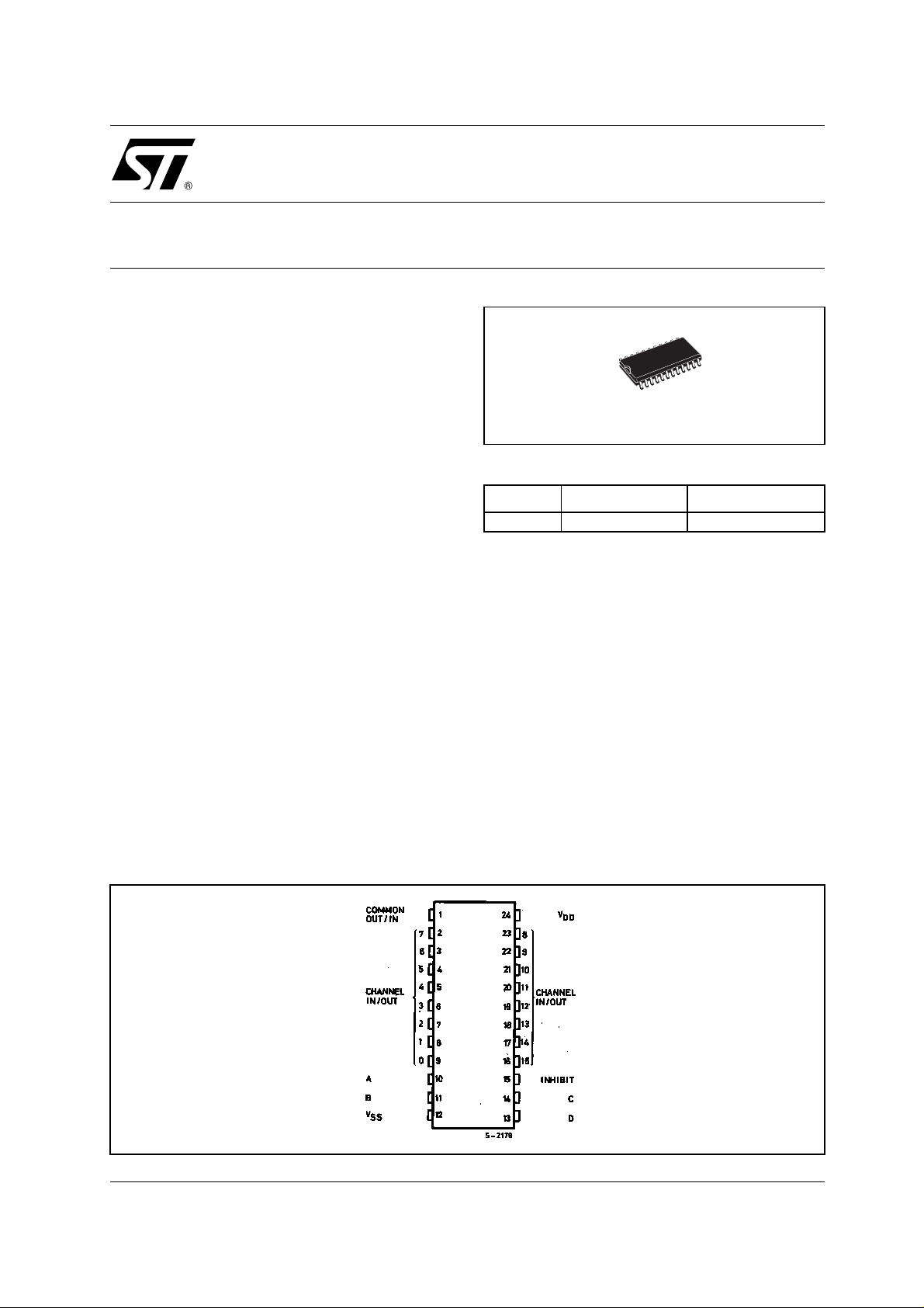
PIN CONNECTION
1/10September 2002
HCF4067B
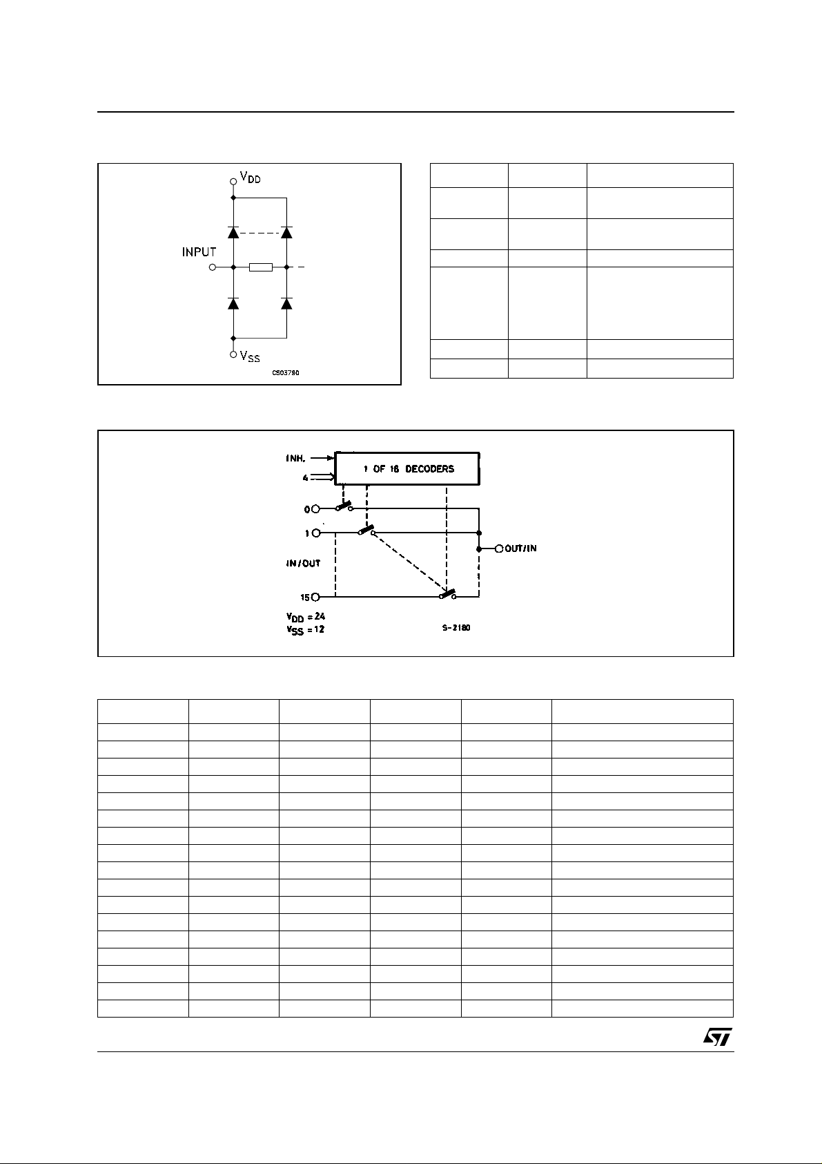
INPUT EQUIVALENT CIRCUIT PIN DESCRIPTION
PIN No SYMBOL NAME AND FUNCTION
10, 11, 14,
13
1
15 INHIBIT Inhibit Input
9, 8, 7, 6, 5,
4, 3, 2, 23,
22, 21, 20,
19, 18, 17,
16
12
24
FUNCTIONAL DIAGRAM
A, B, C, D Binary Control Inputs
COMMON
OUT/IN
0 to 15
CHANNEL
IN/OUT
V
SS
V
DD
Common Out/In
16 channel In/Out
Negative Supply Voltage
Positive Supply Voltage
TRUTH TABLE
A B C D INH SELECTED CHANNEL
X X X X H NONE
LLLLL 0
HLLLL 1
LHLLL 2
HHLLL 3
LLHLL 4
HLHLL 5
LHHLL 6
HHHLL 7
LLLHL 8
HLLHL 9
LHLHL 10
HHLHL 11
LLHHL 12
HLHHL 13
LHHHL 14
HHHHL 15
2/10
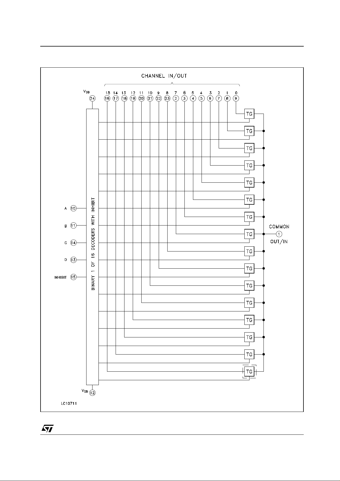
LOGIC DIAGRAM
HCF4067B
3/10

HCF4067B
ABSOLUTE MAXIMUM RATINGS
Symbol Parameter Value Unit
V
V
P
T
T
Absolute Maximum Ratings are those values beyond which damage to the device may occur. Functional operation under these conditions is
not implied.
All voltage values are referred to V
RECOMMENDED OPERATING CONDITIONS
Symbol Parameter Value Unit
V
V
T
Supply Voltage
DD
DC Input Voltage -0.5 to VDD + 0.5
I
I
DC Input Current
I
Power Dissipation per Package 200 mW
D
-0.5 to +22 V
10 mA
±
Power Dissipation per Output Transistor 100 mW
Operating Temperature
op
Storage Temperature
stg
pin voltage.
SS
Supply Voltage
DD
Input Voltage 0 to V
I
Operating Temperature
op
-55 to +125 °C
-65 to +150 °C
3 to 20 V
DD
-55 to 125 °C
V
V
4/10

STATIC ELECTRICAL CHARACTERISTICS
= 25°C,Typical temperature coefficient for all VDD value is 0.3 %/°C)
(T
amb
Test Condition Value
= 25°C
Symbol Parameter
I
Quiescent Supply
L
Current
V
(V)
V
V
IS
EE
(V)
(V)
SS
V
DD
(V)
5 0.04 5 150 150
10 0.04 10 300 300
T
A
Min. Typ. Max. Min. Max. Min. Max.
15 0.04 20 600 600
20 0.08 100 3000 3000
SWITCH
On Resistance
R
ON
Resistance
∆
ON
(between any 2 of
4 switches)
∆
RON
0 < VI
<
V
DD
00
00
5 470 1050 1200 1200
10 180 400 500 520
15 125 240 300 300
510
10 10
15 5
OFF (•) Channel Leakage
Current Any
0018
0.1 100 1000 1000
±
Channel Off
Channel Leakage
Current All
Channel Off
0018
0.1 100 1000 1000
±
(Common Out/In)
C Capacitance Input
5
-5 5
Feedthrough 0.2
CONTROL
Input Low Voltage
V
IL
= VDD
Input High Voltage 5 3.5 3.5 3.5
V
IH
thru
1KΩ
V
= VSS
EE
R
= 1KΩ to
L
V
SS
IIS < 2µA (on
5 1.5 1.5 1.5
15 4 4 4
all OFF
channels)
Input Leakage
I
I
Current
C
Input Capacitance Any Address or Inhibit
I
The Noi se Margin fo r both "1" and "0" level is: 1V min. with VDD=5V, 2V min. with VDD=10V, 2.5V min. with VDD=15V
V
= 0/18V
I
Input
15 11 11 11
18
-3
10
±
5 7.5 pF
• Determ i ned by minimum feasibl e leakage measurement for auto m ating test i ng
-40 to 85°C -55 to 125°C
0.1
±
1
±
HCF4067B
Unit
A
µ
Ω
Ω
A
µ
pFOutput capacitance 55
V10 3 3 3
V10 7 7 7
1
±
A
µ
5/10

HCF4067B
DYNAMIC ELECTRICAL CHARACTERISTICS (T
Symbol Parameter
V
(V)
R
C
(K
Ω)
SWITCH
Propagation Delay
t
pd
Time (Signal Input
to Output)
= V
200 0
DD
Frequency
Response Channel
"ON" (Sine Wave
Input) at
V
20 Log
–––– = -3dB
V
O
I
= V
15 (
DD
Feedthrough (All
channels OFF) at
V
20 Log
V
Frequency Signal
Crosstalk at
V
20 Log
V
Sine Wave
t
W
Distortion (f
1KHz sine wave)
O
––– =-40dB
I
O(A)
––– =-40dB
I(B)
=
IS
= V
V
C(A)
=V
V
C(B)
=V
15 5 (•) 15 0.12
15 (
SS
DD
15 (
SS
5
10 1
CONTROL(Add ress or Inhibit)
t
PLH, tPHL
Propagation Delay
Time:Address or
Inhibit to Signal
10
OUT (Channel
Turning ON)
t
PLH, tPHL
Propagation Delay
Time:Address or
Inhibit to Signal
0.3 0
OUT (Channel
Turning OFF)
Address or Inhibit to
Signal Crosstalk
(*) Typical temperature coefficient for all VDD value is 0.3 %/°C
(**) : Both Ends of Channel
(•) : Peak to Peak voltage s ym m etrical about (V
10** 0 10 75
- VSS) / 2
DD
f
L
I
(KHz)
= 25°C, CL = 50pF, RL = 200KΩ, tr = tf = 20 ns)
amb
Test Condition Value* Unit
VI
VSS
V
(V)
(V)
DD
(V)
Typ. Max.
53060
ns10 15 30
15 11 20
at Common
V
)0 10
•
)0 10
•
O
Out/In
V
at Any Chan-
O
nel
at Common
V
O
Out/In
V
at Any Chan-
O
nel
14
ns
60
20
MHz
8
Between Any two
)0 10
•
(A and B)
1MHz
Channels
2 (•)
50.3
0
%10 3 (•)10 0.2
5 325 650
10 135 270
ns
15 95 190
5 220 440
10 90 180
ns
15 65 130
mV
peak
6/10

HCF4067B
APPLICATION INFORMATION
In applications where separate power sources are
used to drive V
and the signal inputs, the V
DD
DD
current capability should exceed VDD/RL (RL =
effective external load). This provision avoids
permanent current flow or clamp action on the
V
supply when power is applied or removed
DD
from the HCF4067B.
When switching from one address to another,
some of the ON periods of the channels of the
multipl exers will overlap mo mentarily , which ma y
be objectionable in certain applications. Also,
when a channel is turned ON or OFF by an
address input, there is a momentary conductive
path from the channel to V
, which will dump
SS
some charge from any capacitor connec ted to the
input or output of the channel. The inhibit input
turning on a channel will similarly dump some
charge to V
SS
.
The amount of charge dumped is mostly a
function of the signal level above V
- VSS = 10V, a 100 pF capacitor connected to
V
DD
. Typically, at
SS
TEST CIRCUIT
the input or output of the channel will lose 3-4% of
its voltage at the moment the channel turns ON or
OFF. This loss of voltage is essentially
independent of the address or inhibit signal
transition time, if the transition tim e is less th an 12 ms. When the inhibit signal turns a channel off,
there is no change dumping of V
. Rather, there
SS
is a slight rise in the channel voltage level (65 m V
typ.) due to the capacitance coupling from inhibit
input to channel input or output. Address input
also couple some vol tage steps ont o the c hannel
signal levels.
In certain applications, the external load-resistor
current may include both V
components. To avoid drawin g V
and signal line
DD
current when
DD
switch current flows into the transmission gate
inputs, the voltage drop across the bidirectional
switch must not exceed 0.8V (calculated from R
ON
values shown in ELECTRICAL
CHARACTERISTICS CHART). No V
will flow through R
if the switch current flows into
L
current
DD
terminal 1 on the HCF4067B.
CL = 50pF or equivalent (in cludes jig and probe capac i tance)
R
= 200K
Ω
L
R
= Z
of pulse generator (typically 50Ω)
T
OUT
7/10

HCF4067B
WAVEFORM : PROPAGATION DELAY TIMES (f=1MHz; 50% duty cycle)
WAVEFORM : PROPAGATION DELAY TIMES (f=1MHz; 50% duty cycle)
8/10

SO-24 MECHANICAL DATA
HCF4067B
DIM.
MIN. TYP MAX. MIN. TYP. MAX.
A 2.65 0.104
a1 0.1 0.2 0.004 0.008
a2 2.45 0.096
b 0.35 0.49 0.014 0.019
b1 0.23 0.32 0.009 0.012
C 0.5 0.020
c1 45˚ (typ.)
D 15.20 15.60 0.598 0. 614
E 10.00 10.65 0.393 0.419
e 1.27 0.050
e3 13.97 0.550
F 7.40 7.60 0.291 0.300
L 0.50 1.27 0.020 0. 050
S ˚ (max.)
mm. inch
8
L
A
a2
b
e
e3
D
24 13
F
112
a1
c1
b1
C
s
E
PO13T
9/10

HCF4067B
Information furnished is believed to be accurate and reliable. However, STMicroelectronics assumes no responsibi lity f or the
consequences of use of such informatio n nor for any infringement of paten ts or o ther rig hts of t hird part ies which ma y result from
its use. No license is granted by implication or otherwise under any patent or patent rights of STMicroelectronics. Specifications
mentioned in this publication are subject to change without notice. This publication supersedes and replaces all information
previousl y suppl ied. STM icroel ectronics produc ts are not auth orized for use as c ritica l compone nts in l ife s upport dev ices or
systems without express written approval of STMicroelectronics.
Australia - Brazil - Canada - China - Finland - France - Germany - Hong Kong - India - Israel - Italy - Japan - Malaysia - Malta - Morocco
© The ST logo is a registered trademark of STMicroelectronics
© 2002 STMicroelectronics - Printed in Italy - All Rights Reserved
STMicroelectronics GROUP OF COMPANIES
Singapore - Spain - Sweden - Switzerland - United Kingdom - United States.
© http://www.st.com
10/10
 Loading...