

QUAD BILATERAL SWITCH FOR TRANSMISSION OR
MULTIPLEXING OF ANALOG OR DIGITAL SIGNALS
■ 15V DIGITAL OR ±7.5V PEAK TO PEAK
SWITCHING
■ 125Ω TYPICAL ON RESISTANCE FOR 15V
OPERATION
■ SWITCH ON RESISTANCE MATCHED TO
WITHIN 5Ω TYP. OV ER 15V SIGNAL INPUT
RANGE
■ ON RESISTANCE FLAT OVER FULL PEAK
TO PEAK SIGNAL RANGE
■ HIGH ON/OFF OUTPUT VOLTAGERATIO:
65dB TYP. at f
■ HIGH DEGREE OF LINEARITY: < 0.5%
DISTORTION TYP. at f
V
DD-VSS
■ EXTREMELY LOW OFF SWITCH LEAKAGE
RESULTING IN VERY LOW OFFSET
CURRENT AND HIGH EFFECTIVE OFF
RESISTANCE: 10pA T YP.
at V
DD-VSS
■ EXTREMELY HIGH CONTROL INPUT
IMPEDANCE (control circuit isolated from
signal circuit 10
■ LOW CROSSTALK BETWEEN SWITCHES:
50dB Typ. at f
■ MATCHED CONTROL - INPUT TO SIGNAL
OUTPUT CAPACITANCE: REDUCES
OUTPUT SIGNAL TRANSIENTS
■ FREQUENCY RESPONSE SWITCH ON:
40MHz(Typ.)
■ QUIESCENT CURRENT SPECIF. UP TO 20V
■ 5V,10V AND 15V PARAMETRIC RATINGS
= 10KHz, RL= 10KΩ
IS
=1KHz,VIS=5Vpp,
IS
> 10V, R L = 10KΩ
=10V,T
12
Ω typ.)
=0.9MHz,RL=1KΩ
IS
amb
= 25°C
HCF4066B
DIP SOP
ORDER CODES
PACKAGE TUBE T & R
DIP HCF4066BEY
SOP HCF4066BM1 HCF4066M013TR
■ INPUT LEAKAGE CURRENT
I
= 100nA (MAX) AT VDD=18VTA= 25°C
I
■ 100% TESTED FOR QUIESCENT CURRENT
DESCRIPTION
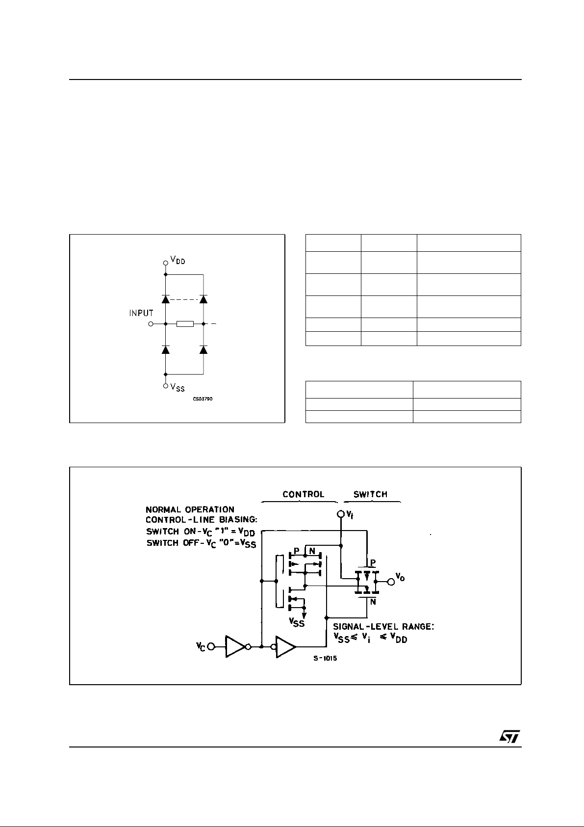
The HCF4066B is a monolithic integrated circuit
fabricated in Metal Oxide Semiconductor
technology available in DIP and SOP packages.
The HCF4066B is a QUAD BILATERAL SWITCH
intended for the transmission or multiplexing of
analog or digital signals.
It is pin for pin compatible with HCF4016 B, but
exhibits a much lower ON resistance. In addition,
the ON resistance is relatively constant over the
full input signal range. The HCF4066B consists of
four independent bilateral switches. A single
control signal is required per switch. Both the p
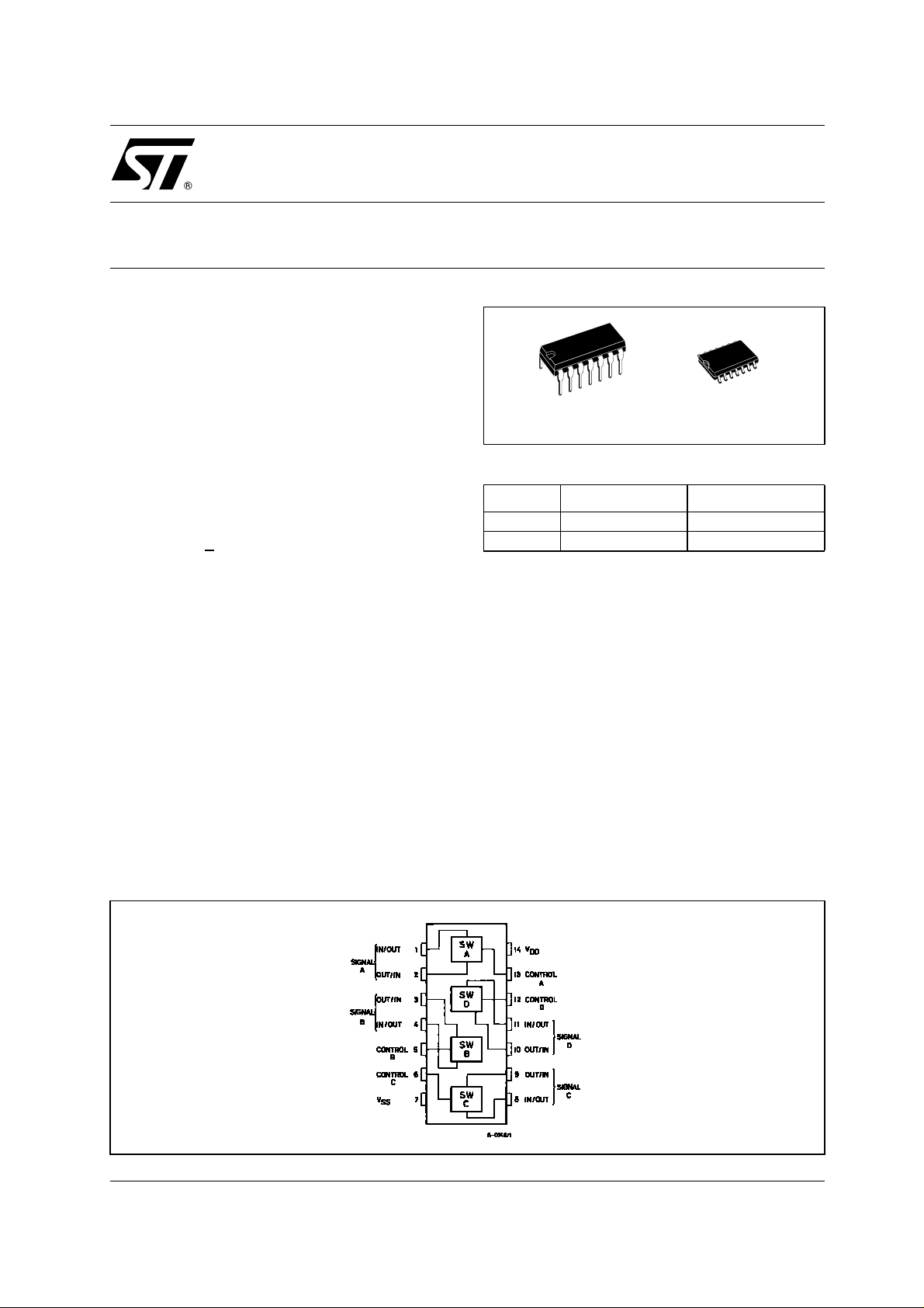
PIN CONNECTION
1/10March 2004
HCF4066B
and n device in a given switch are biased ON or
OFF simultaneously by the control signal. As
shown in schematic diagram, the well of the
n-channel device on each switch is either tied to
theinputwhentheswitchisONortoV
SS
when
include peak input signal voltage swings equal to
the full supply voltage, and more constant ON
impedance over the input signal range . For
sample and hold applications, however, the
HCF4016B is recommended.
the switch is OFF. Thi s c onf iguration eliminates
the variation of the switch-transisto r threshold
voltage with input signal, and thus keeps the ON
resistance low ov er the full operating signal range.
The advant ages over s ingle channel s w it c hes
INPUT EQUIVALENT CIRCUIT PIN DESCRIPTION
PIN N° SYMBOL NAME AND FUNCTION
1, 4, 8, 11 A to D I/O
2, 3, 9, 10 A to D O/I
13,5,6,12
7
14
CONTROL
AtoD
V
V
TRUTH TABLE
SS
DD
Independent Inputs/Outputs
Independent Outputs/
Inputs
Enable Inputs
Negative Supply Voltage
Positive Supply Voltage
CONTROL SWITCH FUNCTION
HON
LOFF
SCHEMATIC DIAGRAM (1 OF 4 IDENTICAL SWITCHES AND ITS ASSOCIATEDCONTROL
CIRCUITY)
2/10
HCF4066B
ABSOLUTE MAXIMUM RATINGS
Symbol Parameter Value Unit
V
V
P
T
T
Absolute Maximum Ratings are those values beyond which damage to the device may occur. Functional operation under these conditions is
not implied.
All voltage values are referred to V
RECOMMENDED OPERATING CONDITIONS
Symbol Parameter Value Unit
V
V
T
Supply Voltage
DD
DC Input Voltage -0.5 to VDD+0.5
I
DC Input Current
I
I
Power Dissipation per Package 200 mW
D
-0.5 to +22 V
± 10 mA
Power Dissipation per Output Transistor 100 mW
Operating Temperature
op
Storage Temperature
stg
pin voltage.
SS
Supply Voltage
DD
Input Voltage 0 to V
I
Operating Temperature
op
-55 to +125 °C
-65 to +150 °C
3to20 V
DD
-55 to 125 °C
V
V
ELECTRICAL CHARACTERISTICS
= 25°C,Typical temperature coefficient for all VDDvalue is 0.3%/°C)
(T
amb
Test Condition Value
Symbol Parameter
I
Quiescent Device
L
Current (all
switches ON or all
switches OFF)
SIGNAL INPUTS (V
Resistance
R
ON
∆
Resistance ∆
ON
)andOUTPUTS(VOS)
IS
RON
(between any 2of
4 switches)
TDH Total Harmonic
Distortion
-3dB Cutoff
Frequency (Switch
on)
-50dBFeedthrough
Frequency (switch
off)
V
I
(V)
0/5 5 0.01 0.25 7.5 7.5
0/10 10 0.01 0.5 15 15
0/15 15 0.01 1 30 30
0/20 20 0.02 5 150 150
V
C=VDDRL
Return to (V
V
IS=VSS
RL=10KΩ,VC=V
V
C=VDD
V
IS
=10KΩ
)/2
DD-VSS
to V
DD
DD
=5V,VSS=-5V
(p-p) = 5V, RL=10KΩ
(sinewavecenteredin0V)
f
=1KHzsinewave
IS
V
C=VDD
V
IS
=5V,VSS=-5V
(p-p) = 5V, RL=1KΩ
(sinewavecenteredin0V)
V
C=VSS
V
(p-p) = 5V, RL=1KΩ
IS
=-5V
(sinewavecenteredin0V)
V
DD
(V)
5 470 1050 1200 1200
15 125 240 300 300
55
15 15
T
Min. Typ. Max. Min. Max. Min. Max.
=25°C
A
-40 to 85°C -55 to 125°C
Unit
µA
Ω10 180 400 500 500
Ω10 10
0.4 %
40 MHz
1MHz
3/10

HCF4066B
Symbol Parameter
-50dB Crosstalk
Frequency
Propagation Delay
t
pd
Time (signal input
to output)
C
Input Capacitance
IS
Output
C
OS
Capacitance
C
Feedthrough 0.5
IOS
Input/Output
Leakage Current
Switch OFF
CONTROL (V
V
ILC
V
IHC
I
I
C
I
)
C
Control Input Low
Voltage
Control Input High
Voltage
Input Leakage
Current
Crosstalk (control
input to signal
output)
Turn - On
Propagation Delay
Time
Control Input
Repetition Rate
Input Capacitance
Test Condition Value
V
I
(V)
V
C(A)=VDD
V
C(B)=VSS
V
IS(A)
50Ω source, R
= 200KΩ, VC=V
R
L
=+5V
=-5V
= 5V (p-p)
=1KΩ
L
DD
VSS=GND,CL= 50pF
V
= 10V
IS
T
V
DD
(V)
A
Min. Typ. Max. Min. Max. Min. Max.
8MHz
20 40
10 20
715
-40 to 85°C -55 to 125°C
=25°C
square wave centered on 5V
t
= 20ns
r,tf
8
V
C=VSS
V
= 18V, VOS=0V
IS
V
=0V,VOS= 18V
IS
=-5
=0V
V
C
+5
18
8
-3
±0.1 ±1 ±1 µA
±10
5111
I
<10µA
IS
V
IS=VSS,VOS=VDD
and
V
IS=VDD,VOS=VSS
15 2 2 2
5 3.5 3.5 3.5
15 11 11 11
VIS< V
VDD-VSS=18V
= 10V (sq. wave)
V
C
t
= 20ns
r,tf
R
= 10KΩ
L
V
IN=VDD,tr,tf
C
= 50pF, RL=1KΩ
L
V
IS=VDD,VSS
R
=1KΩ to GND
L
C
= 50pF, VC= 10V
L
DD
= 20ns
=GND
18
10 50 mV
53570
15 15 30
56
10 9
15 9.5
-5
±0.1 ±1 ±1 µA
±10
sq. wave center on 5V
t
= 20ns
r,tf
V
=1/2VOSat 1KHz
OS
Any Input 5 7.5 pF
Unit
ns
pF
V10 2 2 2
V10 7 7 7
ns10 20 40
MHz
4/10

HCF4066B
TYPICAL APPLICATIONS (BIDIRECTIONAL SIGNAL TRANSMISSION VIADIGITAL CONTROL
LOGIC)
TYPICAL APPLICATIONS (4-CHA NNE L PAM MULTIPLEXER SYSTEM DIAGRAM)
5/10

HCF4066B
TEST CIRCUIT
CL= 50pF or equivalent (includes jig and probe capacitance)
R
=200KΩ
L
R
T=ZOUT
WAVEFORM: PROPAGATION DELAY TIMES (f=1MHz; 50% duty cycle)
of pulse generator (typically 50Ω)
6/10

HCF4066B
Plastic DIP-14 MECHANICAL DATA
mm. inch
DIM.
MIN. TYP MAX. MIN. TYP. MAX.
a1 0.51 0.020
B 1.39 1.65 0.055 0.065
b 0.5 0.020
b1 0.25 0.010
D 20 0.787
E 8.5 0.335
e 2.54 0.100
e3 15.24 0.600
F 7.1 0.280
I 5.1 0.201
L 3.3 0.130
Z 1.27 2.54 0.050 0.100
P001A
7/10

HCF4066B
SO-14 MECHANICAL DATA
DIM.
A 1.75 0.068
a1 0.1 0.2 0.003 0.007
a2 1.65 0.064
b 0.35 0.46 0.013 0.018
b1 0.19 0.25 0.007 0.010
C 0.5 0.019
c1 45˚ (typ.)
D 8.55 8.75 0.336 0.344
E 5.8 6.2 0.228 0.244
e 1.27 0.050
e3 7.62 0.300
F 3.8 4.0 0.149 0.157
G 4.6 5.3 0.181 0.208
L 0.5 1.27 0.019 0.050
M 0.68 0.026
S˚ (max.)
MIN. TYP MAX. MIN. TYP. MAX.
mm. inch
8
8/10
PO13G

HCF4066B
Tape & Reel SO-14 MECHANICAL DATA
mm. inch
DIM.
MIN. TYP MAX. MIN. TYP. MAX.
A 330 12.992
C 12.8 13.2 0.504 0.519
D 20.2 0.795
N 60 2.362
T 22.4 0.882
Ao 6.4 6.6 0.252 0.260
Bo 9 9.2 0.354 0.362
Ko 2.1 2.3 0.082 0.090
Po 3.9 4.1 0.153 0.161
P 7.9 8.1 0.311 0.319
9/10

HCF4066B
Information furnished is believed to be accurate and reliable. However, STMicroelectronics assumes no responsibility for the
consequences of use of such inform ation nor fo r an y infring ement of p atents or o ther rights of third p arties which may r esult f rom
its use. No license is granted by implication or otherwise under any patent or patent rights of STMicroelectronics. Specifications
mentioned in this publication are subject to change without notice. This publication supersedes and replaces all information
previously supplied. STMicroelectronics products are not authorized for use as critical components in life support devices or
systems without express written approval of STMicroelectronics.
Australia - Belgium - Brazil - Canada - China - Czech Republic - Finland - France - Germany - Hong Kong - India - Israel - Italy - Japan -
Malaysia - Malta - Morocco - Singapore - Spain - Sweden - Switzerland - United Kingdom - United States.
The ST logo is a registered trademark of STMicroelectronics
All other names are the property of their respective owners
© 2004 STMicroelectronics - All Rights Reserved
STMicroelectronics GROUP OF COMPANIES
http://www.st.com
10/10
 Loading...