

14-STAGE RIPPLE CARRY BINARY
COUNTER/DIVIDER AND OSCILLATOR
■ MEDIUM-SPEED OPERATION
■ COMMON RESET
■ FULLY STATIC OPERATION
■ BUFFERED INPUTS AND OUTPUTS
■ QUIESCENT CURRENT SPECIFIED UP TO
20V
■ 5V, 10V AND 15V PARAMETRIC RATINGS
■ INPUT LEAKAGE CURRENT
I
= 100nA (MAX) AT VDD=18VTA= 25°C
I
■ 100% TESTED FOR QUIESCENT CURRENT
■ MEETS ALL REQUIREMENTS OF JEDEC
JESD13B "STANDARD SPECIFICATIONS
FOR DESCRIPTION OF B SERIES CMOS
DEVICES"
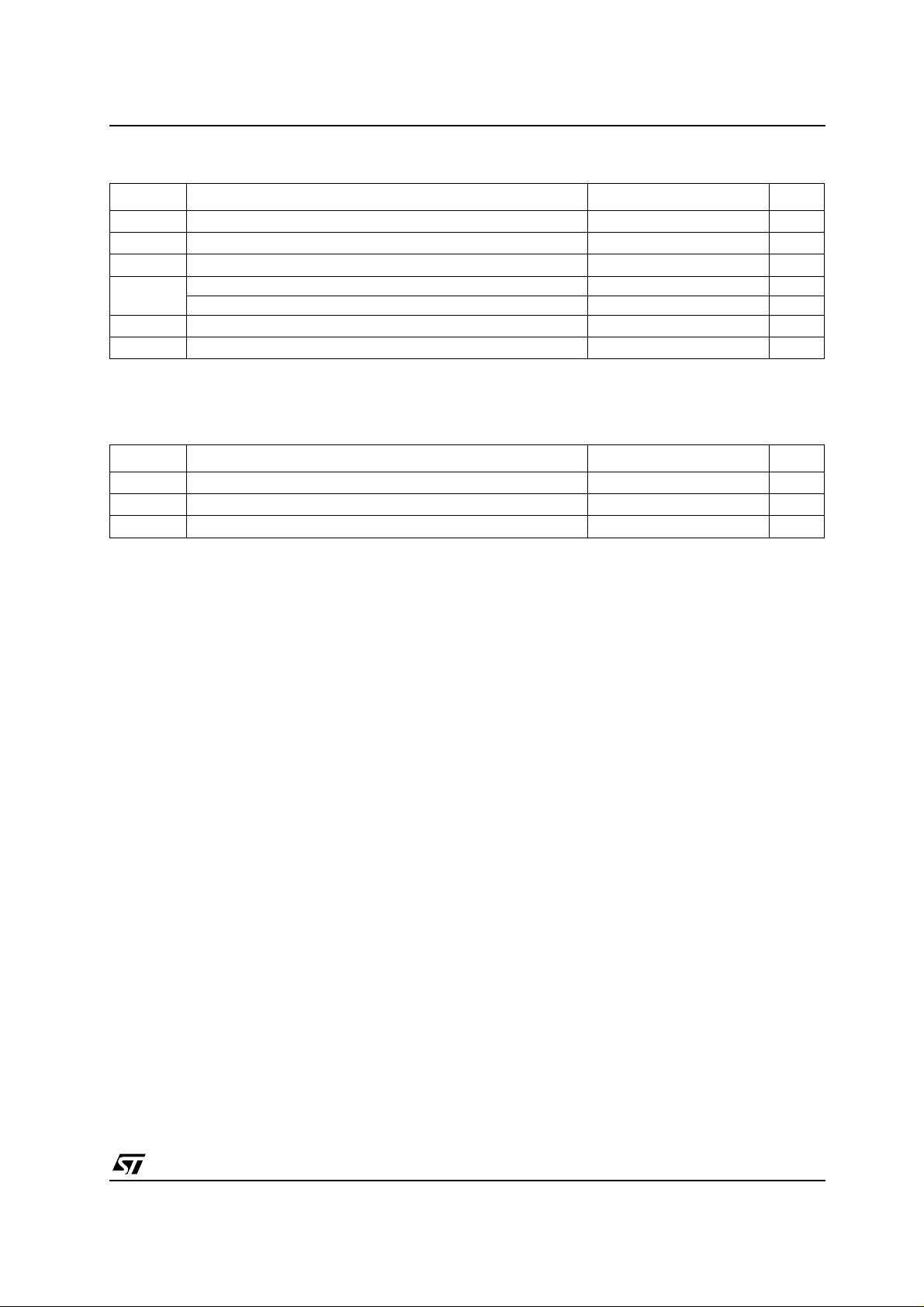
DESCRIPTION
The HCF4060B is a monolithic integrated circuit
fabricated in Metal Oxide Semiconductor
technology available in DIP and SOP packages.
The HCF4060B consists of an oscillator section
and 14 ripple carry binary counter stages.
The oscillator configuration allows design of either
RC or crystal oscillator circuits. A RESET input is
provided which reset the counter to the all 0’s
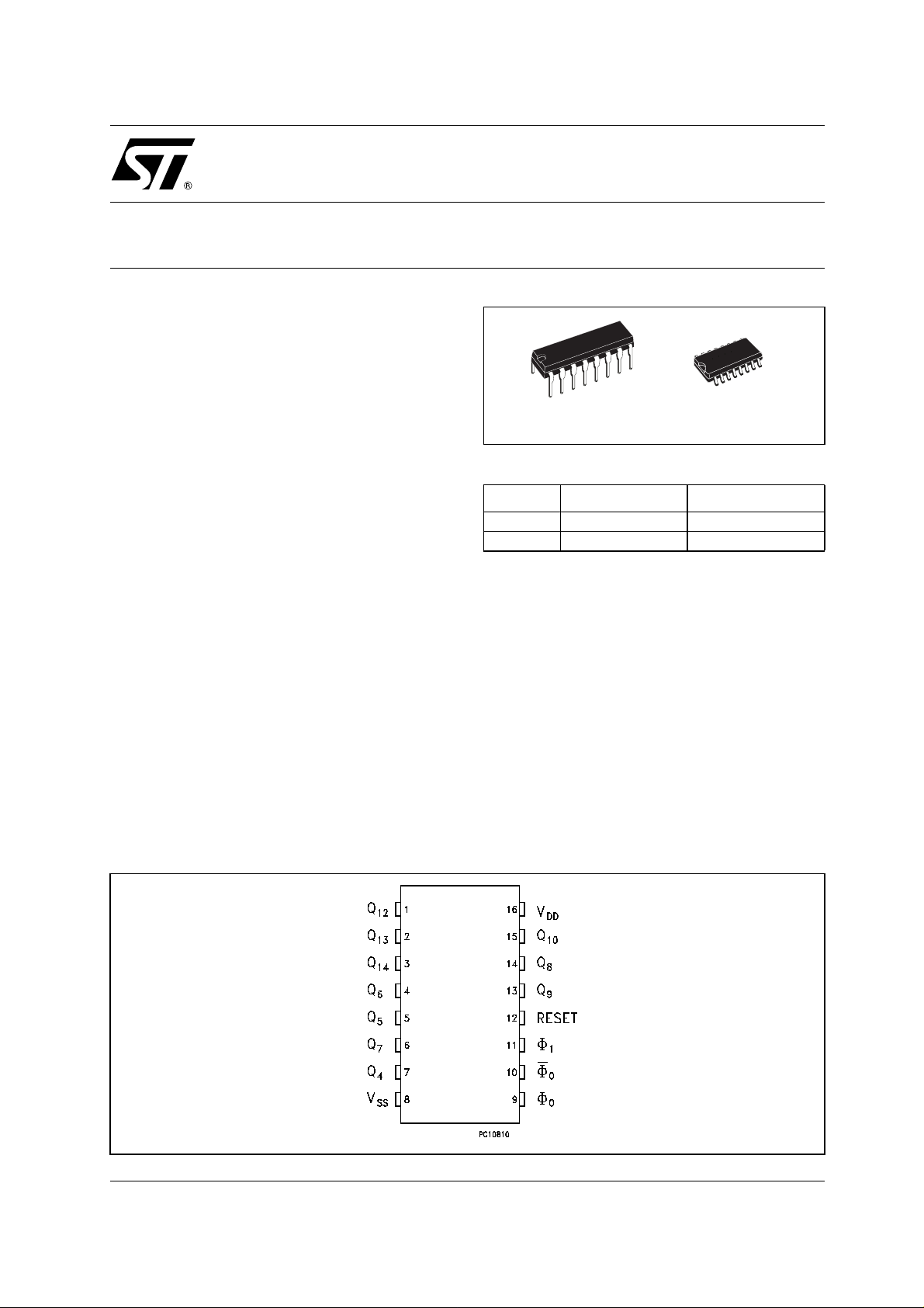
HCF4060B
DIP SOP
ORDER CODES
PACKAGE TUBE T & R
DIP HCF4060BEY
SOP HCF4060BM1 HCF4060M013TR
state and disable oscillator. A high level on the
RESET line accomplishes the reset function. All
counter stages are master slave flip-flops. The
state of t he counter is advanced one step in binary
order on the negative transition o f φ
inputs and outputs are fully buffered. Schmitt
trigger action on the clock pin permits unlimited
clock rise and fall t ime.
(and φ0). All
1
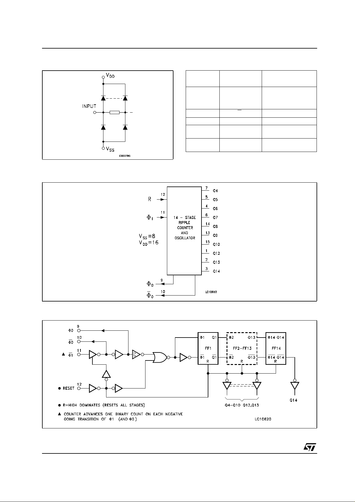
PIN CO NNECTION
1/10August 2003
HCF4060B
INPUT EQUIVALENT CIRCUIT PIN DESCRIPTION
FUNCTIONAL DIAGRAM
PIN No SYMBOL
Q
1, 2, 3, 4,5,
6, 7, 13,14,
15
9, 10, 11
12,Q13,Q14
Q
6,Q5,Q7,Q4
Q
9,Q8,Q10
, Φ0, Φ
Φ
0
12 RESET Reset
8
16
V
SS
V
DD
NAME AND
FUNCTION
,
,
Outputs
Oscillator Input
1
Negative Supply Voltage
Positive Supply Voltage
LOGIC DIAGRAM
2/10
HCF4060B
ABSOLUTE MAXIMUM RATINGS
Symbol Parameter Value Unit
V
V
P
T
T
stg
Absolute Maximum Ratings are those values beyond which damage to the device may occur. Functional operation under these conditions is
not implied.
All voltagevalues arereferredto V
RECOMMENDED OPERATING CONDITIONS
Symbol Parameter Value Unit
V
V
T
Supply Voltage
DD
DC Input Voltage -0.5 to VDD+ 0.5
I
DC Input Current
I
I
Power Dissipation per Package 200 mW
D
-0.5 to +22 V
± 10 mA
Power Dissipation per Output Transistor 100 mW
Operating Temperature
op
Storage Temperature
pin voltage.
SS
Supply Voltage
DD
Input Voltage 0 to V
I
Operating Temperature
op
-55 to +125 °C
-65 to +150 °C
3to20 V
DD
-55 to 125 °C
V
V
3/10

HCF4060B
DC SPECIFICATIONS
Test Condition Value
= 25°C
Symbol Parameter
I
Quiescent Current 0/5 5 0.04 5 5 150
L
V
(V)
|
V
I
O
(V)
|I
O
(µA)
V
DD
(V)
T
A
Min. Typ. Max. Min. Max. Min. Max.
0/10 10 0.04 10 10 300
0/15 15 0.04 20 20 600
0/20 20 0.08 100 100 3000
V
High Level Output
OH
Voltage
0/5 <1 5 4.95 4.95 4.95
0/15 <1 15 14.95 14.95 14.95
V
Low Level Output
OL
Voltage
5/0 <1 5 0.05 0.05 0.05
15/0 <1 15 0.05 0.05 0.05
V
High Level Input
IH
Voltage
0.5/4.5 <1 5 3.5 3.5 3.5
1.5/13.5 <1 15 11 11 11
V
Low Level Input
IL
Voltage
4.5/0.5 <1 5 1.5 1.5 1.5
13.5/1.5 <1 15 4 4 4
I
OH
Output Drive
Current
0/5 2.5 <1 5 -1.36 -3.2 -1.15 -1.1
0/5 4.6 <1 5 -0.44 -1 -0.36 -0.36
0/10 9.5 <1 10 -1.1 -2.6 -0.9 -0.9
0/15 13.5 <1 15 -3.0 -6.8 -2.4 -2.4
I
OL
Output Sink
Current
0/5 0.4 <1 5 0.44 1 0.36 0.36
0/15 1.5 <1 15 3.0 6.8 2.4 2.4
I
Input Leakage
I
Current
Input Capacitance
C
I
The Noise Margin for both "1"and "0"level is:1V min.with VDD=5V, 2V min. with VDD=10V, 2.5V min. with VDD=15V
0/18 Any Input 18
Any Input 5 7.5 pF
±10
-5
-40 to 85°C -55 to 125°C
±0.3 ±0.3 ±1 µA
Unit
µA
V0/10 <1 10 9.95 9.95 9.95
V10/0 <1 10 0.05 0.05 0.05
V1/9 <1 10 7 7 7
V9/1 <1 10 3 3 3
mA
mA0/10 0.5 <1 10 1.1 2.6 0.9 0.9
4/10
HCF4060B
DYNAMIC EL ECTRICAL CHARACTERISTICS (T
= 25° C, CL= 50pF, RL= 200KΩ,tr=tf=20ns)
amb
Test Condition Value (*) Unit
Symbol Parameter
(V)
V
DD
t
TLHtTHL
Output Transition Time 5 100 200
15 40 80
t
PLHtPHL
Propagation Delay Time (φ
out)
to Q
4
5 370 740
15 100 200
t
PLHtPHL
Propagation Delay Time
to Q
(Q
n
n+1
)
5 100 200
15 40 80
t
Input Pulse Width 5
W
f = 100 KHz
15 15 30
t
Input Pulse Rise and Fall
rtf
Time
5
15
f
Maximum Clock Input
max
Frequency
5 3.5 7
15 12 24
RESET OPERATION
t
Propagation Delay Time 5 180 360
PHL
15 50 100
t
Input Pulse Width 5 60 120
W
15 20 40
RC OPERATION
Variation of Frequency
(Unit-to-Unit)
5
C
= 200pF, RS= 560KΩ, RX=50KΩ
X
15 21.1 24 27
Variation of Frequency
With Voltage Change
(Same Unit)
R
X
C
X
Maximum Oscillator
Frequency (**)
(*) Typical temperature coefficient for all VDDvalues is 0.3%/°C, all input rise and fall times= 20 ns.
(**)RCOscillator applications are notrecommendedat supplyvoltagesbelow 7V for R
5to10
= 200pF, RS= 560KΩ, RX=50KΩ
C
X
10 to 15 1
=10µF
5
15
5
15
10
15 690 800 940
C
X
=50µF
C
X
=10µF
C
X
=500KΩ
R
X
=300KΩ
R
X
=300KΩ
R
X
=5KΩ, CX= 15pF
R
X
<50KΩ
X
Min. Typ. Max.
50 100
Unlimited µs10
18 21.5 25
2
20
20
10
1000
50
50
530 650 810
ns10 50 100
ns10 150 300
ns10 50 100
ns10 20 40
MHz10 8 16
ns10 80 160
ns10 30 60
KHz10 20 23 26
KHz
MΩ10
µF10
KHz
5/10

HCF4060B
DETAIL OF TYPICAL FLIP-FLOP STAGE
TYPICAL RC OSCILLATOR CIRCUIT
TYPICAL CRY S TAL OSCILLATOR CIRCUIT
6/10

HCF4060B
Plastic DIP-16 (0.25) MECHANICAL DATA
mm. inch
DIM.
MIN. TYP MAX. MIN. TYP. MAX.
a1 0.51 0.020
B 0.77 1.65 0.030 0.065
b 0.5 0.020
b1 0.25 0.010
D 20 0.787
E 8.5 0.335
e 2.54 0.100
e3 17.78 0.700
F 7.1 0.280
I 5.1 0.201
L 3.3 0.130
Z 1.27 0.050
P001C
7/10
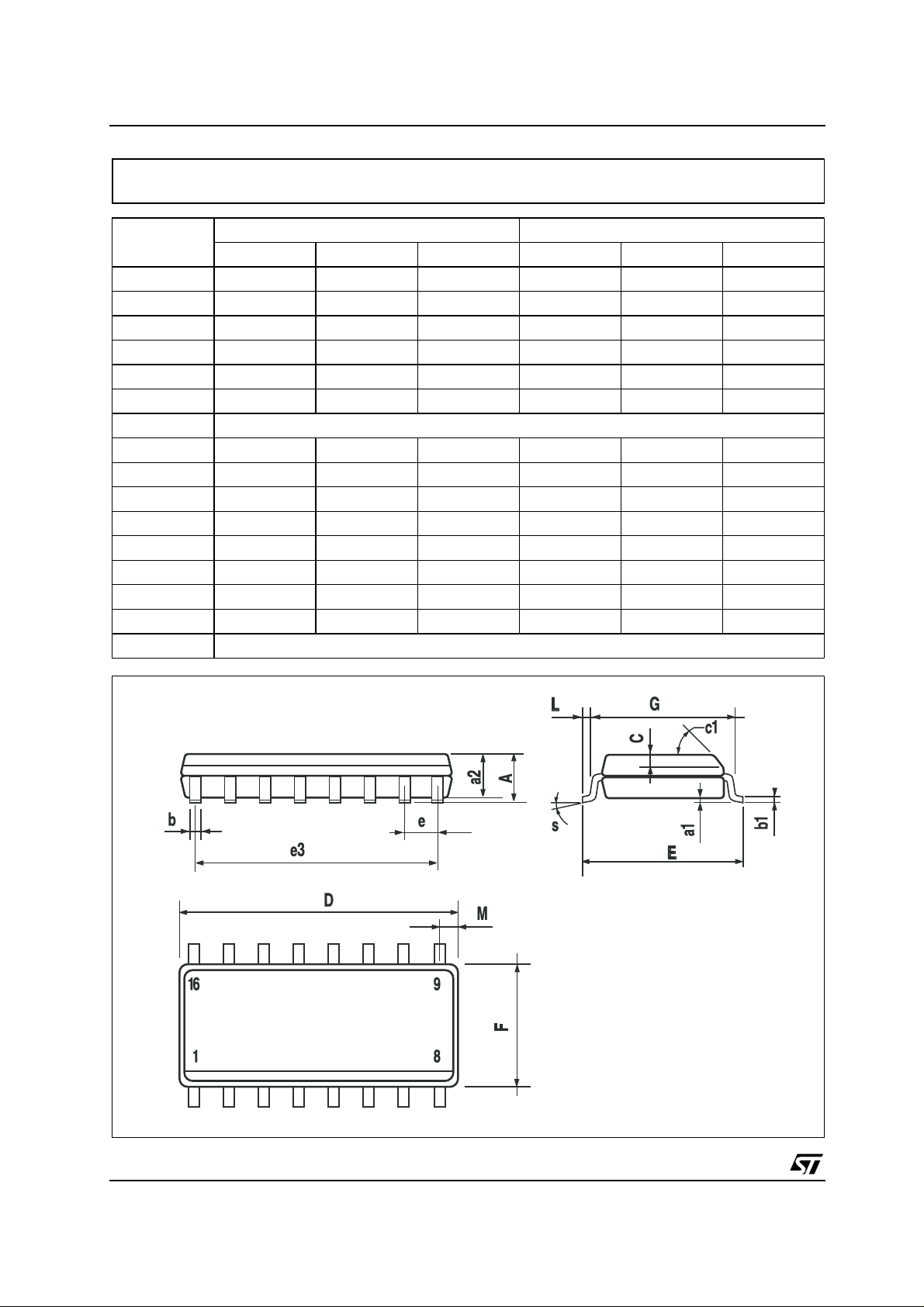
HCF4060B
SO-16 MECHANICAL DATA
DIM.
A 1.75 0.068
a1 0.1 0.2 0.004 0.008
a2 1.65 0.064
b 0.35 0.46 0.013 0.018
b1 0.19 0.25 0.007 0.010
C 0.5 0.019
c1 45˚ (typ.)
D 9.8 10 0.385 0.393
E 5.8 6. 2 0.228 0.244
e 1.27 0.050
e3 8.89 0.350
F 3.8 4.0 0.149 0.157
G 4.6 5.3 0.181 0.208
L 0.5 1.27 0.019 0.050
M 0.62 0.024
S8 ˚ (max.)
MIN. TYP MAX. MIN. TYP. MAX.
mm. inch
8/10
PO13H

HCF4060B
Tape & Reel SO-16 MECHANICAL DATA
mm. inch
DIM.
MIN. TYP MAX. MIN. TYP. MAX.
A 330 12.992
C 12.8 13.2 0.504 0.519
D 20.2 0.795
N 60 2.362
T 22.4 0.882
Ao 6.45 6.65 0.254 0.262
Bo 10.3 10.5 0.406 0.414
Ko 2.1 2.3 0.082 0.090
Po 3.9 4.1 0.153 0.161
P 7.9 8.1 0.311 0.319
9/10

HCF4060B
Information furnished is believed to be accurate and reliable. However, STMicroelectronics assumes no responsibility for the
consequences of use o f suc h inf ormat ion n or f or an y infr ingeme nt of paten ts or oth er ri gh ts of third part ies whic h may resul t f rom
its use. No license is granted by implication or otherwise under any patent or patent rights of STMicroelectronics. Specifications
mentioned in this publication are subject to change without notice. This publication supersedes and replaces all information
previously supplied. STMicroelectronics products are not authorized for use as critical components in life support devices or
systems without express written approval of STMicroelectronics.
Australia - Brazil - Canada - China - Finland - France - Germany - Hong Kong - India - Israel - Italy - Japan - Malaysia - Malta - Morocco
© The ST logo is a registered trademark of STMicroelectronics
© 2003 STMicroelectronics - Printed in Italy - All Rights Reserved
STMicroelectronics GROUP OF COMPANIES
Singapore - Spain - Sweden - Switzerland - United Kingdom - United States.
© http://www.st.com
10/10
 Loading...