

HCF4047B
LOW POWER MONOSTABLE/ASTA BLE MULTIVIBRATOR
■ LOW POWER CONSUMPTION : SPECIAL
CMOS OSCILLATOR CONFIGURATION
■ MONOSTABLE (one - shot) OR ASTABLE
(free-running) OPERATION
■ TRUE AND COMPLEMENTED BUFFERED
OUTPUTS
■ ONLY ONE EXTERNAL R AND C REQUIRED
■ BUFFERED INPUTS
■ QUIESCENT CURRENT SPECIFIED UP TO
20V
■ STANDARD IZED, SYMMETRIC AL OUTPUT
CHARACTERISTIC S
■ 5V, 10V AND 15V PARAMETRIC RAT INGS
■ INPUT LEAKAGE CURRENT
I
= 100nA (MAX) AT VDD = 18V TA = 25°C
I
■ 100% TESTED FOR QUIESCENT CURRENT
■ MEETS ALL REQUIREMENTS OF JEDEC
JESD13B " STANDARD SPECIF ICATIONS
FOR DESCRIPTI ON OF B SERI ES CMOS
DEVICES"
DESCRIPTION
The HCF4047B is a m onolithic integrated circuit
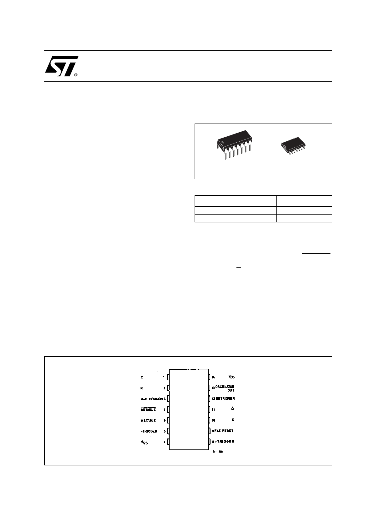
fabricated in Metal Oxide Semiconductor
technology available in DIP and SOP packages.
The HCF4047B consist of a gatable astable
multivibrator with logic techniques i nc orporated to
DIP SOP
ORDER CODES
PACKAGE TUBE T & R
DIP HCF4047BEY
SOP HCF4047BM1 HCF4047M013TR
permit positive or negative edge-triggered
monostable multivibrator action with retriggering
and external counting options. Inputs include
+TRIGGER -TRIGGER, ASTABLE, ASTABLE
RETRIGGER, and EXTERNAL RESET. Buffe red
outputs are Q, Q
and OSCILLATOR. In all modes
of operation, an external capacitor must be
connected between C-Timing and RC-Common
terminals, and an external resistor must be
connected between the R-Timing and
RC-Common terminals.
For operating modes see functional terminal
connections and application notes.
,
PIN CONNECTION
1/12September 2001
HCF4047B
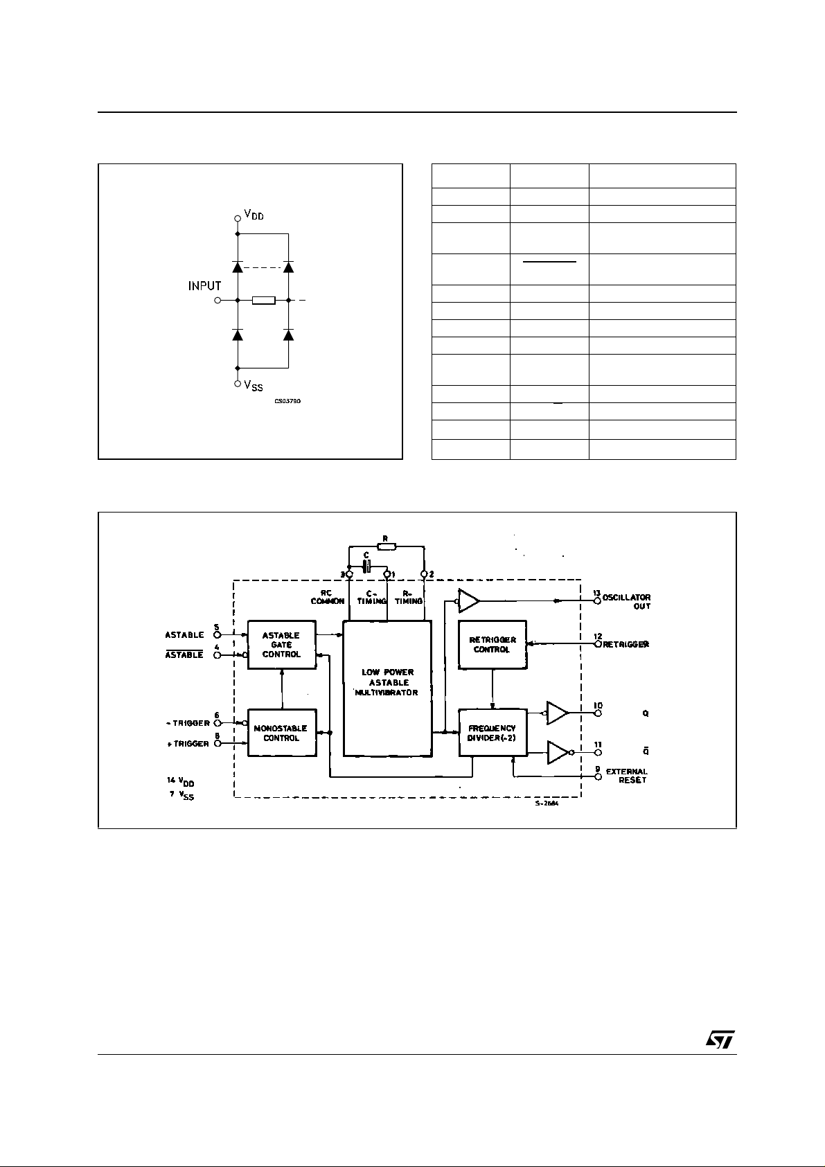
INPUT EQUIVALENT CIRCUIT PIN DESCRIPTION
PIN No SYMBOL NAME AND FUNCTION
1 C External Capacitor
2 R External Resistor
3
4 ASTABLE
5 ASTABLE True Astable Pulse
6 -TRIGGER Negative Trigger Pulse
8 +TRIGGER Positive Trigger Pulse
9 EXT. RESET External Reset
12
13 OSC. OUT Oscillator Output
10,11 Q, Q
7
14
RC COM-
MON
RETRIG-
GER
V
SS
V
DD
BLOCK DIAGRAM
External Connection to (1)
and (2)
Complement Astable
Pulse
Retrigger Mode Pulse
Q Outputs
Negative Supply Voltage
Positive Supply Voltage
2/12
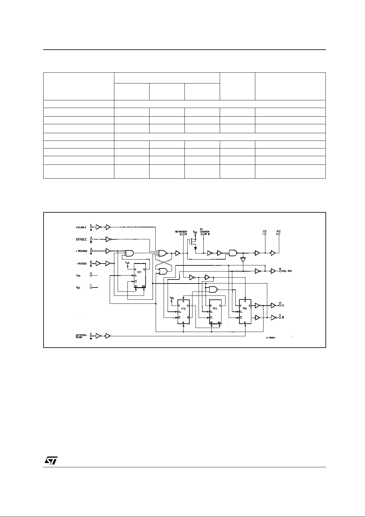
FUNCTIONAL TERMINAL CONNECTIONS
HCF4047B
FUNCTION*
TERMINAL CONNECTIONS
to V
DD
to V
SS
Input Pulse
to
OUTPUT
PULSE
FROM
OUTPUT PERIOD OR
Astable Multivibrator
Free Running 4, 5, 6, 14 7, 8, 9, 12 - 10, 11, 13 t
True Gating 4, 6, 14 7, 8, 9, 12 5 10, 11, 13
Complement Gating 6, 14 5, 7, 8, 9, 12 4 10, 11, 13 t
Monostable Multivibrator
Positive - Edge Trigger 4, 14 5, 6, 7, 9, 12 8 10, 11
Negative - Edge Trigger 4, 8, 14 5, 7, 9, 12 6 10, 11
Retriggerable 4, 14 5, 6, 7, 9 8, 12 10, 11 t
External Countdown** 14 5, 6, 7, 8, 9,
- 10, 11
12
* In all case s external c apacitor and resistor between pins, 1, 2 and 3 (see logic diagrams).
** Input pulse to Reset of External Counting Chip.
External Counting Chip Output to pin 4.
LOGIC DIAGRAM
PULSE WIDTH
(10,11) = 4.40RC
A
(13) = 2.20RC
A
(10,11) = 2.48RC
M
3/12
HCF4047B
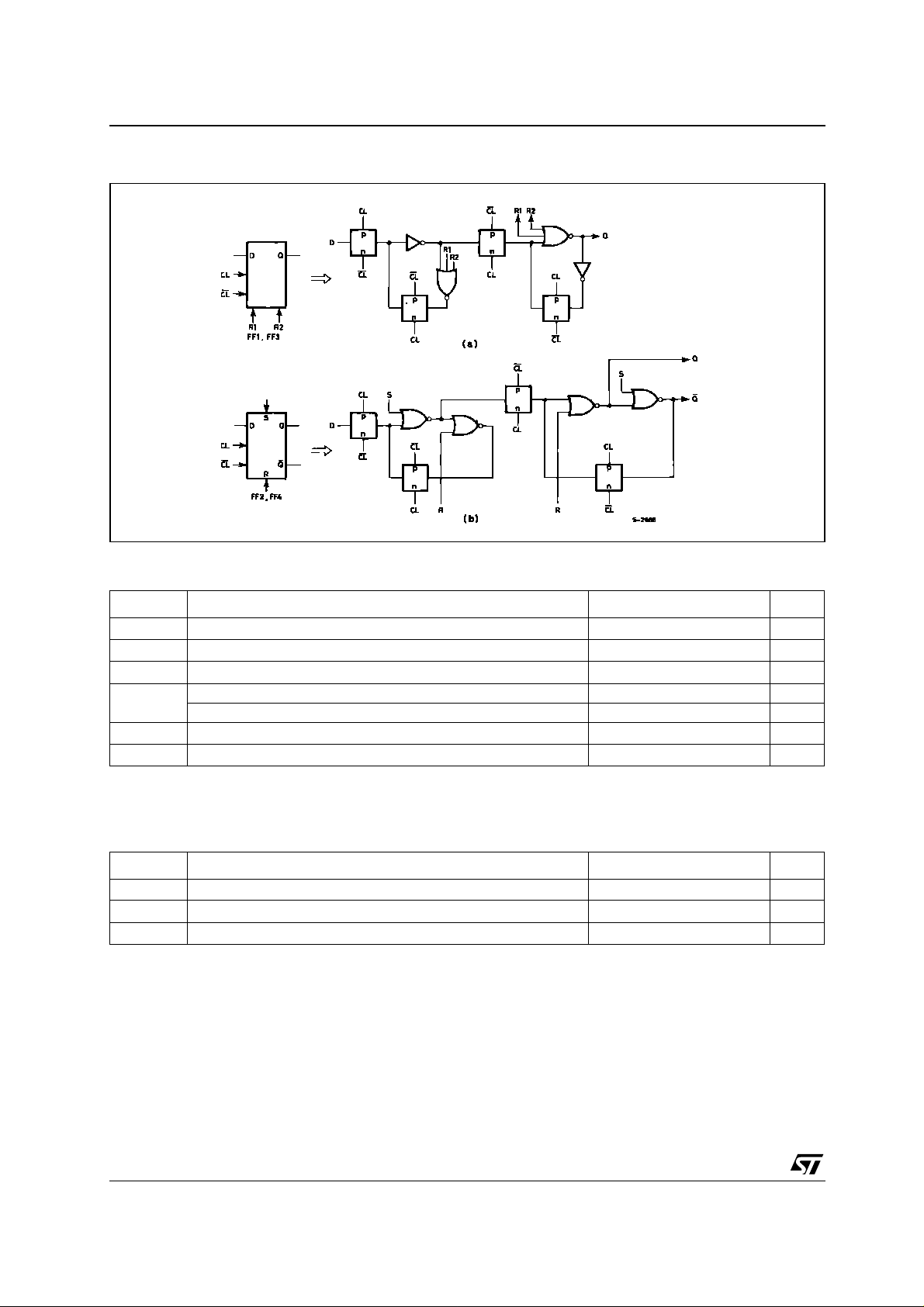
DETAIL FOR FLIP-FLOPS FF1 AND FF3 (a) AND FOR FLIP-FLOPS FF2 AND FF4 (b)
ABSOLUTE MAXIMUM RATINGS
Symbol Parameter Value Unit
V
V
P
Supply Voltage
DD
DC Input Voltage -0.5 to VDD + 0.5
I
I
DC Input Current
I
Power Dissipation per Package 200 mW
D
-0.5 to +22 V
± 10 mA
V
Power Dissipation per Output Transistor 100 mW
T
T
Absolute Maximum Ratings are those values beyond which damage to the device may occur. Functional operation under these conditions is
not implied.
All voltage value s are referred to V
Operating Temperature
op
Storage Temperature
stg
pin voltage.
SS
-55 to +125 °C
-65 to +150 °C
RECOMMENDED OPERATING CONDITIONS
Symbol Parameter Value Unit
V
V
T
Supply Voltage
DD
Input Voltage 0 to V
I
Operating Temperature
op
3 to 20 V
DD
-55 to 125 °C
V
4/12

DC SPECIFICATIONS
Test Condition Value
T
Symbol Parameter
I
Quiescent Current 0/5 5 0.01 1 30 30
L
V
(V)
V
I
(V)
|I
|
O
O
(µA)
V
DD
(V)
= 25°C
A
Min. Typ. Max. Min. Max. Min. Max.
0/10 10 0.01 2 60 60
0/15 15 0.01 4 120 120
0/20 20 0.02 20 600 600
V
High Level Output
OH
Voltage
0/5 <1 5 4.95 4.95 4.95
0/15 <1 15 14.95 14.95 14.95
Low Level Output
V
OL
Voltage
5/0 <1 5 0.05 0.05 0.05
15/0 <1 15 0.05 0.05 0.05
High Level Input
V
IH
Voltage
0.5/4.5 <1 5 3.5 3.5 3.5
1.5/13.5 <1 15 11 11 11
V
IL
Low Level Input
Voltage
4.5/0.5 <1 5 1.5 1.5 1.5
13.5/1.5 <1 15 4 4 4
I
OH
Output Drive
Current
0/5 2.5 <1 5 -1.36 -3.2 -1.15 -1.1
0/5 4.6 <1 5 -0.44 -1 -0.36 -0.36
0/10 9.5 <1 10 -1.1 -2.6 -0.9 -0.9
0/15 13.5 <1 15 -3.0 -6.8 -2.4 -2.4
I
OL
Output Sink
Current
0/5 0.4 <1 5 0.44 1 0.36 0.36
0/15 1.5 <1 15 3.0 6.8 2.4 2.4
Input Leakage
I
I
Current
C
Input Capacitance
I
The Noi se Margin for both "1" and " 0" level is: 1V min. wit h VDD=5V, 2V min. with VDD=10V, 2.5V min. with VDD=15V
0/18 Any Input 18
Any Input 5 7.5 pF
±10
-5
-40 to 85°C -55 to 125°C
±0.1 ±1 ±1 µA
HCF4047B
Unit
µA
V0/10 <1 10 9.95 9.95 9.95
V10/0 <1 10 0.05 0.05 0.05
V1/9 <1 10 7 7 7
V9/1 <1 10 3 3 3
mA
mA0/10 0.5 <1 10 1.1 2.6 0.9 0.9
5/12

HCF4047B
DYNAMIC ELECTRICAL CHARACTERISTICS (T
Symbol Parameter
t
PLH tPHL
t
THL tTLH
t
(*) Typical temper at ure coeffic i ent for all VDD value is 0.3 %/°C.
Propagation Delay
Time
Transition Time Osc. Out Q, Q 5 100 200
Input Pulse Width + Trigger
t
W
, tfInput Rise and Fall Time All Inputs 5
r
Deviation from 50% Duty
Q or Q
Factor
Astable, Astable
to Osc. Out
Astable, Astable
to Q, Q
+ or - Trigger to
Q, Q
Retrigger to Q, Q
External Reset
to Q, Q
- Trigger
Reset 5 100 200
Retrigger 5 300 600
V
DD
10 100 200
15 80 160
10 175 350
15 125 250
10 225 4 50
15 150 3 00
10 150 300
15 100 200
10 100 200
15 70 140
15 40 80
10 80 160
15 50 100
10 50 100
15 30 60
10 115 230
15 75 150
15
15 ±0.1 ±0.5
APPLICATION INFORMATION
1 - CIRCUIT DESCRIPTION
Astable operation is enabled by a high level on the
ASTABLE input. The period of the square wave at
the Q and Q
Outputs in this mode of operation is a
function of the external components employed.
"True" input pulses on the ASTABLE input or
"Complement" pulses on the ASTABLE
input
allow the circuit to be used as a gatable
multivibrator. The OSCILLATOR output period will
be half of the Q terminal output in the astable
mode. However, a 50% duty cycle is not
guaranteed at this output. In the monostable
6/12
= 25°C, CL = 50pF, RL = 200KΩ, tr = tf = 20 ns)
amb
Test Condition Value (*) Unit
(V)
5 200 400
5 350 700
5 500 1000
5 300 600
5 250 500
5 200 400
5 ±0.5 ±1
Min. Typ. Max.
Unlimited µs10
mode, positive-edge triggering is accomplished by
application of a leading-edge pulse to the
+TRIGGER input and a low level to the -TRIGGER
input. For negative-edge triggering, a trailing-edge
pulse is applied to the -TRIGGER and a high level
is applied to the +TRIGGER. Input pulses m ay be
of any duration relative to the output pulse. The
multivibrator can be retriggered (on the leading
edge only) by applying a com mon pulse to both
the RETRIGGER and +TRIGGER inputs. In this
mode the output pulse remains high as long as the
input pulse period is shorter than the period
determined by the RC components. An external
countdown option can be implemented by
ns
ns10 50 100
ns
%10 ±0.5 ±1

HCF4047B
coupling "Q" to an external "N" counter and
resetting the counter with the trigger pulse. The
counter output pulse is fed ba ck to the ASTAB LE
input and has a duration equal to N times the
period of the multivibrator. A high level on the
EXTERNAL RESET input assures no output pulse
during an "ON" power condition. This input can
also be activated to terminate the output pulse at
any time. In the mono stable mo de, a high-le vel or
ASTABLE MODE WAVEFORMS
power-on reset pulse, must be applied to the
EXTERNAL RESET whenever V
is applied .
DD
2 - ASTABLE MODE
The following analysis presents worst-case
variations from unit-to-unit as a function of
transfer-voltage (VTR) shift (33% - 67% V
DD
free-running (astable) operation.
V
t1 = -RC In —————
V
VDD - V
t2 = -RC In —————
2V
(VTR)(VDD - VTR)
= 2(t1+t2)= -2RC In ———————————
t
3
(V
DD
DD
TR
+ V
- V
TR
TR
TR
+ VTR)(2VDD - VTR)
DD
) for
Typ : V
Min : V
Max : V
thus if t
= 0.5 VDD tA = 4.40 RC
TR
= 0.33 VDD tA = 4.62 RC
TR
= 0.67 VDD tA = 4.62 RC
TR
= 4.40 RC is used, the maximum
A
variation will be (+ 5.0%, -0.0%)
In addition to variations from unit-to-unit, the
astable period may vary as a function of frequency
with respect to V
and temperature.
DD
MONOSTABLE WAVEFORMS
3 - MONOSTABLE MODE
The following analysis presents worst-case
variations from unit-to-unit as a function of
transfer-voltage (V
) shift (33% - 67% VDD) for
TR
one-shot (monostable) operation.
V
t1 = -RC In ———
2V
VDD - V
t2 = -RC In —————
2V
(VTR)(VDD - VTR)
t
= (t1+t2)= -RC In —————————
M
(2V
TR
DD
DD
- V
TR
TR
- VTR)(2VDD)
DD
7/12

HCF4047B
Where tM = monostable mode pulse width. Values
for tM are as follows :
Typ : V
Min : V
Max : V
Thus if t
= 0.5 VDD tM = 2.48 RC
TR
= 0.33 VDD tM = 2.71 RC
TR
= 0.67 VDD tM = 2.48 RC
TR
= 2.48 RC is used, the maximum
M
variation will be (+ 9.3%, - 0.0%).
Note : In the astable mode, the first positive half
cycle has a duration of T
are t
/2.
A
; succeeding durations
M
In addition to variations from unit to unit, the
monostable pulse width m ay vary as a f unction of
frequency with respect to V
and temperature.
DD
4 - RETRIGGER MODE
The HCF4047B can be used in the retrigger mode
FIGURE A : Retrigger-mode waveforms
to extend the output-pulse duration, or to compare
the frequency of an input signal with that of the
internal oscillator. In the retrigger mode the input
pulse is applied to terminals 8 and 12, and the
output is taken from terminal 10 or 11. As shown in
fig.A normal monostable action is obt ained when
one retrigger pulse is applied. Extended pulse
duration is obtained when more than one pulse is
applied. For two in put pulses, t
For more than two pulses, t
terminates at some variable time t
termination of the last retrigger pulse. t
because t
(Q OUTPUT) terminates after the
RE
= t1’ + t1 + 2t2.
RE
(Q OUTPUT)
RE
after the
D
is variable
D
second positive edge of the oscillator output
appears at flip-flop 4 (see logic diagram).
5 - EXTERNAL COUNTER OPTION
A typical implement ation is shown in fig. B. T he
pulse duration at the output is
Time t
can be extended by any am ount with the
M
use of external counting circuitry. Advantages
include digitally controlled pulse duration, small
text = (N - 1) (t
Where text = pulse duration of the circuitry, and N
is the number of counts used.
timing capacitors for long time periods, and
extremely fast recovery ti me.
FIGURE B : Implementation of external counter option
) + (tM + tA/2)
A
8/12

HCF4047B
6 - POWER CONSUMPTION
In the standby mode (Monostable or Astable),
power dissipation will be a function of leakage
current in the circuit, as shown in the static
electrical characteristics. For dynamic operation,
the power needed to charge the external timing
capacitor C is given by the following formula :
Astable Mode :
P = 2CV
P = 4CV
(2.9CV
Monostable Mode : P = ——————————
T
(Output at Pin 10 and 11)
2
f. (Output at Pin 13)
2
f. (Output at Pin 10 and 11)
2
) (Duty Cycle)
The circuit is designed so that most of the total
power is consumed in the external components. In
practice, the lower the values of frequency and
voltage used, the closer the actual power
dissipation will be to the calculated value.
Because the power dissipation does not depend
on R, a design for minimum power dissipation
would be a small value of C. The value of R would
depend on the desired period (within the
limitations discussed above).
7 - TIMING-COMPONENT LIMITATIONS
TEST CIRCUIT
The capacitor used in the circuit should be
non-polarized and have low leakage (i.e. the
parallel resistance of t he capacitor should be an
order of magnitude greater than the external
resistor used). Three is n o up per or lower limit for
either R or C value to maintain oscillation.
However, in consideration of accuracy, C must be
much larger than the inherent stray capacitance in
the system (unless this capacitance can be
measured and taken into account). R must be
much larger than the COS/MOS "ON" resistance
in series with it, which typically is hundreds of
ohms. In addition, with very large values of R,
some short-term instability with respect to time
may be noted.
The recommended valu es for these components
to maintain agreement with previously c alculated
formulas without trimming should be :
C >
100pF, up to any practical value, for astable
modes ;
C >
1000pF, up to any practical value, for
monostable modes.
10KΩ<
R < 1MΩ.
CL = 50pF or equivalent (in cl udes jig and probe capac i tance)
R
= 200KΩ
L
R
= Z
of pulse generator (typically 50Ω)
T
OUT
9/12

HCF4047B
Plastic DIP-14 MECHANICAL DATA
mm. inch
DIM.
MIN. TYP MAX. MIN. TYP. MAX.
a1 0.51 0.020
B 1.39 1.65 0.055 0.065
b 0.5 0.020
b1 0.25 0.010
D 20 0.787
E 8.5 0.335
e 2.54 0.100
e3 15.24 0.600
F 7.1 0.280
I 5.1 0.201
L 3.3 0.130
Z 1.27 2.54 0.050 0.100
10/12
P001A

SO-14 MECHANICAL DATA
HCF4047B
DIM.
A 1.75 0.068
a1 0.1 0.2 0.003 0.007
a2 1.65 0.064
b 0.35 0.46 0.013 0.018
b1 0.19 0.25 0.007 0.010
C 0.5 0.019
c1 45° (typ.)
D 8.55 8.75 0.336 0.344
E 5.8 6.2 0.228 0.244
e 1.27 0.050
e3 7.62 0.300
F 3.8 4.0 0.149 0.157
G 4.6 5.3 0.181 0.208
L 0.5 1.27 0.019 0.050
M 0.68 0.026
S8° (max.)
MIN. TYP MAX. MIN. TYP. MAX.
mm. inch
PO13G
11/12

HCF4047B
Information furnished is bel ieved to be accurate and reliable. However, STMicroe lectronics assumes no responsibility for the
consequences of use of such information nor for any infringement of patents or other rights of third parties which may result from
its use. No li cense is granted by i mp lica tion or otherwise under a ny patent or patent rights of STMicroelec tronics. Specifications
mentioned in this publication ar e subject to change without notice. This publication supersedes and replaces all information
previously supplied. S TMicroelectronics products are not authorized for use as critica l components in life suppo rt devices or
systems without express written approval of STMicroelectronics.
Australi a - Brazil - C hi na - Finlan d - F rance - Germ any - Hong Kong - India - Italy - Japan - Malaysia - Ma l ta - Morocco
© The ST logo is a registered trademark of STMicroelectronics
© 2001 STM icroelectronics - Printed in Italy - All Ri g h ts Reserv ed
STMicr o el ectronics G ROU P OF COMPANI E S
Singapo re - Spain - Sweden - Swi t zerland - United Kingdom
© http://www.st.com
12/12
 Loading...