

HCF4042B
QUAD CLOCKED D LATCH
■ CLOCK POLARITY CONTROL
■ Q AND Q OUTP U TS
■ COMMON CLOCK
■ LOW POWER TTL COMPATIBLE
■ STANDARDIZED SYMMETRICAL OUTPUT
CHARACTERISTICS
■ QUIESCENT CURRENT SPECIFIED UP TO
20V
■ 5V, 10V AND 15V PARAMETRIC RATINGS
■ INPUT LEAKAGE CURRENT
I
= 100nA (MAX) AT VDD = 18V TA = 25°C
I
■ 100% TESTED FOR QUIESCENT CURRENT
■ MEETS ALL REQUIREMENTS OF JEDEC
JESD13B " STANDARD SPECIFICATIONS
FOR DESCRIPTI ON OF B SERI ES CMOS
DEVICES"
DESCRIPTION
The HCF4042B is a m onolithic integrated circuit
fabricated in Metal Oxide Semiconductor
technology available in DIP and SOP packages.
The HCF4042B types c ontains four latch circuit,
each strobes by a common clock. Complementary
buffered outputs are available from each circuit.
The impedance of the n and p channel output
devices is balanced and all outputs are electrically
identical.
DIP SOP
ORDER CODES
PACKAGE TUBE T & R
DIP HCF4042BEY
SOP HCF4042BM1 HCF4042M013TR
Information present at the data input is transferred
to outputs Q and Q
during the CLOCK level which
is programmed by the POLARITY input. For
POLARITY = 0 the transfer occurs during the 0
CLOCK level a nd for POLARITY = 1 the transfer
occurs during the 1 CLOCK level. The outputs
follow the data input providing the CLOCK and
POLARITY levels defined above are present.
When a CLOCK transition occurs (positive for
POLARITY = 0 and nega tive for POLARITY = 1)
the information present at the input during the
CLOCK transition is retained at the outputs until
an opposite CLOCK transition occurs.
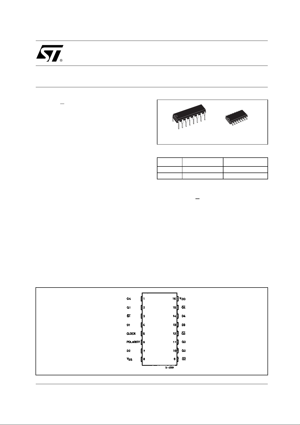
PIN CONNECTION
1/9September 2001
HCF4042B
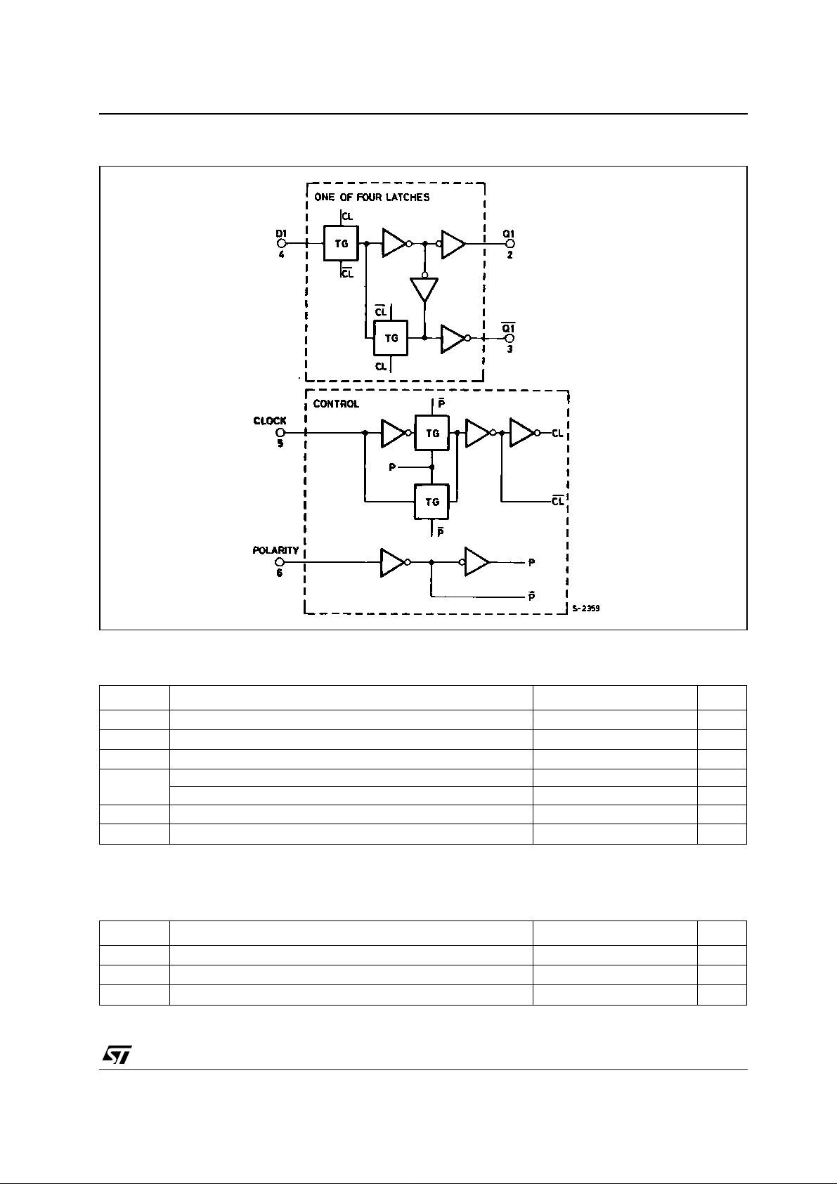
IINPUT EQUIVALENT CIRCUIT PIN DESCRIPTION
PIN No SYMBOL NAME AND FUNCTION
4, 7, 13, 14 D1 to D4 Data Inputs
2, 10, 11, 1 Q1 to Q4 Q outputs
3, 9, 12, 15 Q1
5 CLOCK Clock Input
6 POLARITY Polarity inputs
8
16
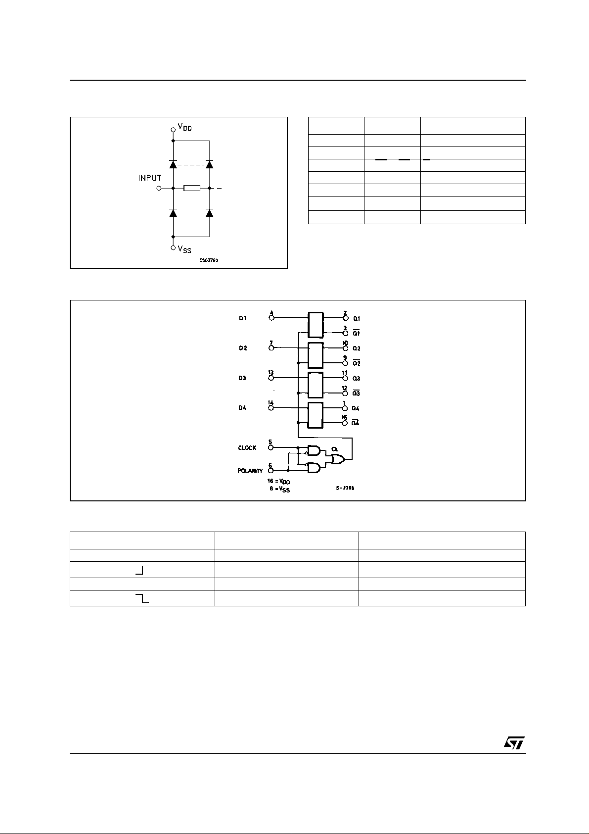
FUNCTIONAL DIAGRAM
to Q4 Q outputs
V
SS
V
DD
Negative Supply Voltage
Positive Supply Voltage
TRUTH TABLE
CLOCK POLARITY Q
L0 D
H1 D
2/9
0LATCH
1LATCH
LOGIC BLOCK DIAGRAM
HCF4042B
This log i c diagram has not be used to est i m ate propagation dela ys
ABSOLUTE MAXIMUM RATINGS
Symbol Parameter Value Unit
V
V
P
Supply Voltage
DD
DC Input Voltage -0.5 to VDD + 0.5
I
I
DC Input Current
I
Power Dissipation per Package 200 mW
D
-0.5 to +22 V
± 10 mA
V
Power Dissipation per Output Transistor 100 mW
T
T
Absolute Maximum Ratings are those values beyond which damage to the device may occur. Functional operation under these conditions is
not implied.
All voltage values are referred to V
Operating Temperature
op
Storage Temperature
stg
pin voltage.
SS
-55 to +125 °C
-65 to +150 °C
RECOMMENDED OPERATING CONDITIONS
Symbol Parameter Value Unit
V
V
T
Supply Voltage
DD
Input Voltage 0 to V
I
Operating Temperature
op
3 to 20 V
DD
-55 to 125 °C
V
3/9

HCF4042B
DC SPECIFICATIONS
Test Condition Value
T
Symbol Parameter
I
Quiescent Current 0/5 5 0.02 1 30 30
L
V
(V)
V
I
(V)
|I
|
O
O
(µA)
V
DD
(V)
= 25°C
A
Min. Typ. Max. Min. Max. Min. Max.
0/10 10 0.02 2 60 60
0/15 15 0.02 4 120 120
0/20 20 0.04 20 600 600
V
High Level Output
OH
Voltage
0/5 <1 5 4.95 4.95 4.95
0/15 <1 15 14.95 14.95 14.95
Low Level Output
V
OL
Voltage
5/0 <1 5 0.05 0.05 0.05
15/0 <1 15 0.05 0.05 0.05
High Level Input
V
IH
Voltage
0.5/4.5 <1 5 3.5 3.5 3.5
1.5/13.5 <1 15 11 11 11
V
IL
Low Level Input
Voltage
4.5/0.5 <1 5 1.5 1.5 1.5
13.5/1.5 <1 15 4 4 4
I
OH
Output Drive
Current
0/5 2.5 <1 5 -1.36 -3.2 -1.1 -1.1
0/5 4.6 <1 5 -0.44 -1 -0.36 -0.36
0/10 9.5 <1 10 -1.1 -2.6 -0.9 -0.9
0/15 13.5 <1 15 -3.0 -6.8 -2.4 -2.4
I
OL
Output Sink
Current
0/5 0.4 <1 5 0.44 1 0.36 0.36
0/15 1.5 <1 15 3.0 6.8 2.4 2.4
Input Leakage
I
I
Current
C
Input Capacitance
I
The Noi se Margin fo r both "1" and "0" level is: 1V min. with VDD=5V, 2V min. with VDD=10V, 2.5V min. with VDD=15V
0/18 Any Input 18
Any Input 5 7.5 pF
±10
-5
-40 to 85°C -55 to 125°C
±0.1 ±1 ±1 µA
Unit
µA
V0/10 <1 10 9.95 9.95 9.95
V10/0 <1 10 0.05 0.05 0.05
V1/9 <1 10 7 7 7
V9/1 <1 10 3 3 3
mA
mA0/10 0.5 <1 10 1.1 2.6 0.9 0.9
4/9

HCF4042B
DYNAMIC ELECTRICAL CHARACTERISTICS (T
Symbol Parameter
t
PLH tPHL
t
PLH tPHL
t
PLH tPHL
t
PLH tPHL
t
THL tTLH
t
setup
t
t
(*) Typical temperature coefficient for all VDD value is 0.3 %/°C.
Propagation Delay Time
(DATA IN to Q)
Propagation Delay Time
(DATA IN to Q
)
Propagation Delay Time
(CLOCK to Q)
Propagation Delay Time
(CLOCK to Q
)
Transition Time 5 100 200
Clock Pulse Width 5 200 100
t
W
Setup Time 5 50 0
Hold Time 5 120 60
hold
, tf Input Pulse Rise and Fall
r
Time
(V)
V
DD
5 110 220
15 40 80
5 150 300
15 50 100
5 225 450
15 80 160
5 250 500
15 90 180
15 40 80
15 60 30
15 25 0
15 50 25
5
15
= 25°C, CL = 50pF, RL = 200KΩ, tr = tf = 20 ns)
amb
Test Condition Value (*) Unit
Min. Typ. Max.
ns10 55 110
ns10 75 150
ns10 100 200
ns10 115 230
ns10 50 100
ns10 100 50
ns10 30 0
ns10 60 30
Not Rise or Fall
Time Sensitive
µs10
5/9

HCF4042B
TEST CIRCUIT
CL = 50pF or equivalent (in cludes jig and probe capac i t ance)
= 200KΩ
R
L
R
= Z
of pulse generator (typically 50Ω)
T
OUT
6/9

HCF4042B
Plastic DIP-16 (0.25) MECHANICAL DATA
mm. inch
DIM.
MIN. TYP MAX. MIN. TYP. MAX.
a1 0.51 0.020
B 0.77 1.65 0.030 0.065
b 0.5 0.020
b1 0.25 0.010
D 20 0.787
E 8.5 0.335
e 2.54 0.100
e3 17.78 0.700
F 7.1 0.280
I 5.1 0.201
L 3.3 0.130
Z 1.27 0.050
P001C
7/9

HCF4042B
SO-16 MECHANICAL DATA
DIM.
A 1.75 0.068
a1 0.1 0.2 0.003 0.007
a2 1.65 0.064
b 0.35 0.46 0.013 0.018
b1 0.19 0.25 0.007 0.010
C 0.5 0.019
c1 45° (typ.)
D 9.8 10 0.385 0.393
E 5.8 6.2 0.228 0.244
e 1.27 0.050
e3 8.89 0.350
F 3.8 4.0 0.149 0.157
G 4.6 5.3 0.181 0.208
L 0.5 1.27 0.019 0.050
M 0.62 0.024
S8° (max.)
MIN. TYP MAX. MIN. TYP. MAX.
mm. inch
8/9
PO13H

HCF4042B
Information furnished is bel ieved to be accurate and reliable. However, STMicroe lectronics assumes no responsibility for the
consequences of use of such information nor for any infringement of patents or other rights of third parties which may result from
its use. No li cense is granted by i mp lication or otherwise under any patent or patent rights of STMicroelectronics. Specifications
mentioned in this publication ar e subject to change without notice. This publication supersedes and replaces all information
previously supplied. S TMicroelectronics products are not authorized for use as critica l components in life suppo rt devices or
systems without express written approval of STMicroelectronics.
Australi a - Brazil - Chi na - Finlan d - F rance - Germ any - Hong Kong - India - Ital y - Japan - Ma l aysia - Malta - Morocco
© The ST logo is a registered trademark of STMicroelectronics
© 2001 STM icroelectronics - P rinted in Italy - All Righ ts Reserv ed
STMicr o el ectronics GROUP OF COMPA NI ES
Singapo re - Spain - Sweden - Switzerland - United Ki ngdom
© http://www.st.com
9/9
 Loading...