

HCF4030B
QUAD EXCLUSIVE-OR GATE
■ MEDIUM SPEED OPERATION - t
65ns (TYP.) at CL = 50pF and V
■ LOW OUTPUT IMPEDANCE : 500 Ω (TYP. ) at
V
DD-VSS =
■ QUIESCENT CURRENT SPECIFIED UP TO
10V
= t
PHL
DD-VSS =
PLH =
10V
20V
■ 5V, 10V AND 15V PARAMETRIC RAT INGS
■ INPUT LEAKAGE CURRENT
I
= 100nA (MAX) AT VDD = 18V TA = 25°C
I
■ 100% TESTED FOR QUIESCENT CURRENT
■ MEETS ALL REQUIREMENTS OF JEDEC
JESD13B "STANDARD SPECIFICATIONS
FOR DESCRIPTI ON OF B SERI ES CMOS
DEVICES"
DESCRIPTION
HCF4030B is a monolithic integrated circuit
fabricated in Metal Oxide Semiconductor
technology available in DIP and SOP packages.
HCF4030B types consist of four indipendent
exclusive-OR gates integrated on a single
monolithic silicon chip. Each exclusive-OR gate
consists of four n-channel and four p-channel
enhancement-type transistors. All inputs and
outputs are protected against electrostatic effects.
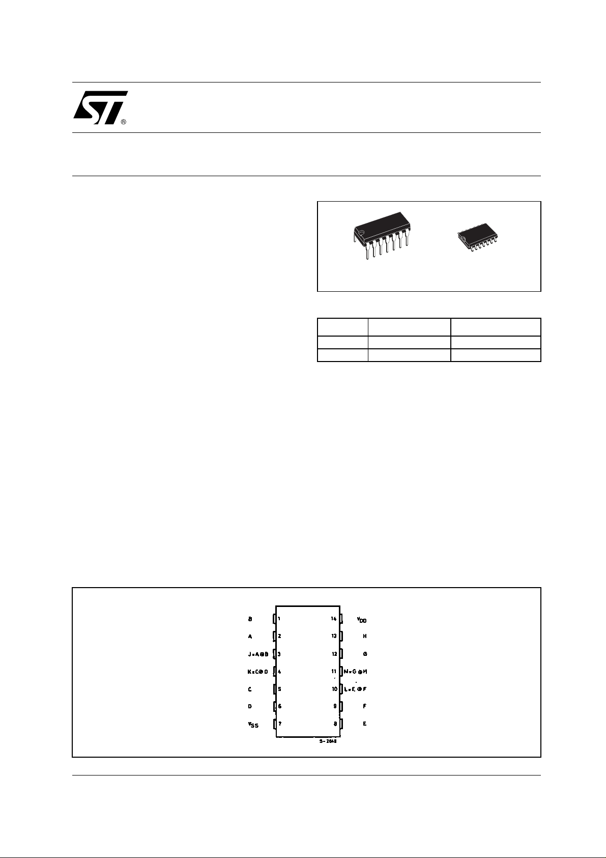
DIP SOP
ORDER CODES
PACKAGE TUBE T & R
DIP HCF4030BEY
SOP HCF4030BM1 HCF4030M013TR
PIN CONNECTION
1/10September 2002
HCF4030B
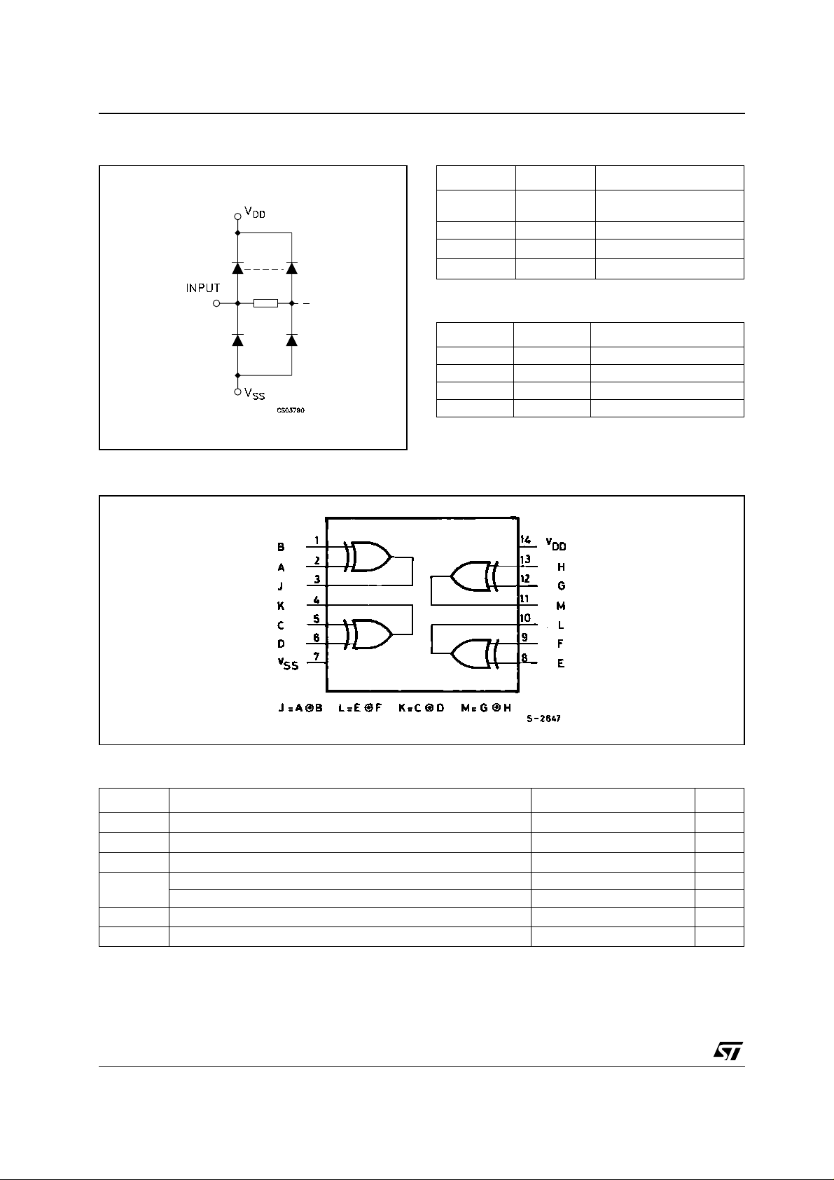
INPUT EQUIVALENT CIRCUIT PIN DESCRIPTION
PIN No SYMBOL NAME AND FUNCTION
2, 1, 5, 6, 8,
9, 12, 13
3, 4, 10, 11 J, K, L, M Data Outputs
7
14
TRUTH TABLE
IN1 IN2 OUT
LL L
LH H
HL H
HH L
FUNCTIONAL DIAGRAM
A, B, C, D, E,
F, G, H
V
SS
V
DD
Data Inputs
Negative Supply Voltage
Positive Supply Voltage
ABSOLUTE MAXIMUM RATINGS
Symbol Parameter Value Unit
V
V
P
T
T
Absolute Maximum Ratings are those values beyond which damage to the device may occur. Functional operation under these conditions is
not implied.
All voltage values are referred to V
2/10
Supply Voltage
DD
DC Input Voltage -0.5 to VDD + 0.5
I
I
DC Input Current
I
Power Dissipation per Package 200 mW
D
-0.5 to +22 V
10 mA
±
Power Dissipation per Output Transistor 100 mW
Operating Temperature
op
Storage Temperature
stg
pin voltage.
SS
-55 to +125 °C
-65 to +150 °C
V
HCF4030B
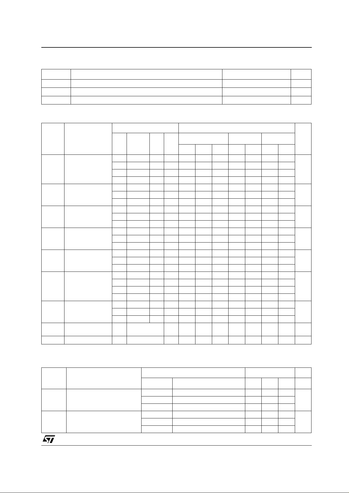
RECOMMENDED OPERATING CONDITIONS
Symbol Parameter Value Unit
V
V
T
DC SPECIFICATIONS
Symbol Parameter
I
L
V
OH
V
OL
V
IH
V
IL
I
OH
I
OL
I
I
C
I
The Noi se Margin for bot h " 1" and "0" level is: 1V min. wit h VDD=5V, 2V min. with VDD=10V, 2.5V min. with VDD=15V
Supply Voltage
DD
Input Voltage 0 to V
I
Operating Temperature
op
3 to 20 V
DD
-55 to 125 °C
Test Condition Value
V
(V)
T
|
V
I
O
(V)
|I
O
(µA)
V
DD
(V)
A
Min. Typ. Max. Min. Max. Min. Max.
-40 to 85°C -55 to 125°C
= 25°C
Quiescent Current 0/5 5 0.02 4 4 30
0/10 10 0.02 8 8 60
0/15 15 0.02 16 16 120
0/20 20 0.04 20 20 600
Output High
0/5 <1 5 4.95 4.95 4.95
Voltage
0/15 <1 15 14.95 14.95 14.95
Output Low Voltage 5/0 <1 5 0.05 0.05 0.05
15/0 <1 15 0.05 0.05 0.05
Input High Voltage 0.5/4.5 <1 5 3.5 3.5 3.5
1.5/13.5 <1 15 11 11 11
Input Low Voltage 4.5/0.5 <1 5 1.5 1.5 1.5
13.5/1.5 <1 15 4 4 4
Output Drive
Current
0/5 2.5 <1 5 -1.36 -3.2 -1.15 -1.1
0/5 4.6 <1 5 -0.44 -1 -0.36 -0.36
0/10 9.5 <1 10 -1.1 -2.6 -0.9 -0.9
0/15 13.5 <1 15 -3.0 -6.8 -2.4 -2.4
Output Sink
0/5 0.4 <1 5 0.44 1 0.36 0.36
Current
0/15 1.5 <1 15 3.0 6.8 2.4 2.4
Input Leakage
Current
Input Capacitance
0/18 Any Input 18
Any Input 5 7.5 pF
-5
0.1
±
10
±
1
±
1
±
V
Unit
A
µ
V0/10 <1 10 9.95 9.95 9.95
V10/0 <1 10 0.05 0.05 0.05
V1/9 <1 10 7 7 7
V9/1 <1 10 3 3 3
mA
mA0/10 0.5 <1 10 1.1 2.6 0.9 0.9
A
µ
DYNAMIC ELECTRICAL CHARACTERISTICS (T
Symbol Parameter
t
PLH tPHL
t
TLH tTHL
Propagation Delay Time 5 140 280
Output Transition Time 5 100 200
V
(V)
DD
15 50 100
15 40 80
= 25°C, CL = 50pF, RL = 200KΩ, tr = tf = 20 ns)
amb
Test Condition Value (*) Unit
Min. Typ. Max.
ns10 65 130
ns10 50 100
3/10
 Loading...